EP1191363A1 - Optical waveplate and optical device using the waveplate - Google Patents
Optical waveplate and optical device using the waveplate Download PDFInfo
- Publication number
- EP1191363A1 EP1191363A1 EP01306797A EP01306797A EP1191363A1 EP 1191363 A1 EP1191363 A1 EP 1191363A1 EP 01306797 A EP01306797 A EP 01306797A EP 01306797 A EP01306797 A EP 01306797A EP 1191363 A1 EP1191363 A1 EP 1191363A1
- Authority
- EP
- European Patent Office
- Prior art keywords
- waveplate
- optical
- waveguide
- pen
- film
- Prior art date
- Legal status (The legal status is an assumption and is not a legal conclusion. Google has not performed a legal analysis and makes no representation as to the accuracy of the status listed.)
- Withdrawn
Links
- 230000003287 optical effect Effects 0.000 title claims abstract description 34
- 239000011112 polyethylene naphthalate Substances 0.000 claims abstract description 29
- 229920003207 poly(ethylene-2,6-naphthalate) Polymers 0.000 claims abstract description 26
- -1 polyethylene naphthalate Polymers 0.000 claims description 4
- 239000004642 Polyimide Substances 0.000 abstract description 9
- 229920001721 polyimide Polymers 0.000 abstract description 9
- 239000010408 film Substances 0.000 description 11
- 239000011888 foil Substances 0.000 description 8
- 230000010287 polarization Effects 0.000 description 6
- 230000008033 biological extinction Effects 0.000 description 5
- 229920000642 polymer Polymers 0.000 description 5
- 239000000463 material Substances 0.000 description 4
- 235000012431 wafers Nutrition 0.000 description 4
- XUIMIQQOPSSXEZ-UHFFFAOYSA-N Silicon Chemical compound [Si] XUIMIQQOPSSXEZ-UHFFFAOYSA-N 0.000 description 3
- 238000001125 extrusion Methods 0.000 description 3
- 229920000139 polyethylene terephthalate Polymers 0.000 description 3
- 239000005020 polyethylene terephthalate Substances 0.000 description 3
- 229910052710 silicon Inorganic materials 0.000 description 3
- 239000010703 silicon Substances 0.000 description 3
- VYPSYNLAJGMNEJ-UHFFFAOYSA-N Silicium dioxide Chemical compound O=[Si]=O VYPSYNLAJGMNEJ-UHFFFAOYSA-N 0.000 description 2
- 238000004891 communication Methods 0.000 description 2
- 238000010586 diagram Methods 0.000 description 2
- 238000000034 method Methods 0.000 description 2
- 230000008569 process Effects 0.000 description 2
- 239000000758 substrate Substances 0.000 description 2
- 239000010409 thin film Substances 0.000 description 2
- 239000004229 Alkannin Substances 0.000 description 1
- 229920002799 BoPET Polymers 0.000 description 1
- 239000001879 Curdlan Substances 0.000 description 1
- 239000005041 Mylar™ Substances 0.000 description 1
- 239000004235 Orange GGN Substances 0.000 description 1
- 239000001825 Polyoxyethene (8) stearate Substances 0.000 description 1
- 239000001882 Soybean hemicellulose Substances 0.000 description 1
- 229920006125 amorphous polymer Polymers 0.000 description 1
- 230000008901 benefit Effects 0.000 description 1
- 230000000052 comparative effect Effects 0.000 description 1
- 239000004148 curcumin Substances 0.000 description 1
- 230000000694 effects Effects 0.000 description 1
- 230000009477 glass transition Effects 0.000 description 1
- PEDCQBHIVMGVHV-UHFFFAOYSA-N glycerol Substances OCC(O)CO PEDCQBHIVMGVHV-UHFFFAOYSA-N 0.000 description 1
- 230000006872 improvement Effects 0.000 description 1
- 229920000728 polyester Polymers 0.000 description 1
- 229920006254 polymer film Polymers 0.000 description 1
- 239000004172 quinoline yellow Substances 0.000 description 1
- 230000009467 reduction Effects 0.000 description 1
- 239000002151 riboflavin Substances 0.000 description 1
- 239000000377 silicon dioxide Substances 0.000 description 1
- 239000002904 solvent Substances 0.000 description 1
- 239000000600 sorbitol Substances 0.000 description 1
- 238000004528 spin coating Methods 0.000 description 1
- 239000000126 substance Substances 0.000 description 1
- 239000000213 tara gum Substances 0.000 description 1
Images


Classifications
-
- G—PHYSICS
- G02—OPTICS
- G02B—OPTICAL ELEMENTS, SYSTEMS OR APPARATUS
- G02B6/00—Light guides; Structural details of arrangements comprising light guides and other optical elements, e.g. couplings
- G02B6/10—Light guides; Structural details of arrangements comprising light guides and other optical elements, e.g. couplings of the optical waveguide type
- G02B6/12—Light guides; Structural details of arrangements comprising light guides and other optical elements, e.g. couplings of the optical waveguide type of the integrated circuit kind
- G02B6/12007—Light guides; Structural details of arrangements comprising light guides and other optical elements, e.g. couplings of the optical waveguide type of the integrated circuit kind forming wavelength selective elements, e.g. multiplexer, demultiplexer
- G02B6/12009—Light guides; Structural details of arrangements comprising light guides and other optical elements, e.g. couplings of the optical waveguide type of the integrated circuit kind forming wavelength selective elements, e.g. multiplexer, demultiplexer comprising arrayed waveguide grating [AWG] devices, i.e. with a phased array of waveguides
- G02B6/12011—Light guides; Structural details of arrangements comprising light guides and other optical elements, e.g. couplings of the optical waveguide type of the integrated circuit kind forming wavelength selective elements, e.g. multiplexer, demultiplexer comprising arrayed waveguide grating [AWG] devices, i.e. with a phased array of waveguides characterised by the arrayed waveguides, e.g. comprising a filled groove in the array section
-
- G—PHYSICS
- G02—OPTICS
- G02B—OPTICAL ELEMENTS, SYSTEMS OR APPARATUS
- G02B5/00—Optical elements other than lenses
- G02B5/30—Polarising elements
- G02B5/3083—Birefringent or phase retarding elements
-
- G—PHYSICS
- G02—OPTICS
- G02B—OPTICAL ELEMENTS, SYSTEMS OR APPARATUS
- G02B6/00—Light guides; Structural details of arrangements comprising light guides and other optical elements, e.g. couplings
- G02B6/10—Light guides; Structural details of arrangements comprising light guides and other optical elements, e.g. couplings of the optical waveguide type
- G02B6/105—Light guides; Structural details of arrangements comprising light guides and other optical elements, e.g. couplings of the optical waveguide type having optical polarisation effects
-
- G—PHYSICS
- G02—OPTICS
- G02B—OPTICAL ELEMENTS, SYSTEMS OR APPARATUS
- G02B6/00—Light guides; Structural details of arrangements comprising light guides and other optical elements, e.g. couplings
- G02B6/10—Light guides; Structural details of arrangements comprising light guides and other optical elements, e.g. couplings of the optical waveguide type
- G02B6/12—Light guides; Structural details of arrangements comprising light guides and other optical elements, e.g. couplings of the optical waveguide type of the integrated circuit kind
- G02B6/12007—Light guides; Structural details of arrangements comprising light guides and other optical elements, e.g. couplings of the optical waveguide type of the integrated circuit kind forming wavelength selective elements, e.g. multiplexer, demultiplexer
- G02B6/12009—Light guides; Structural details of arrangements comprising light guides and other optical elements, e.g. couplings of the optical waveguide type of the integrated circuit kind forming wavelength selective elements, e.g. multiplexer, demultiplexer comprising arrayed waveguide grating [AWG] devices, i.e. with a phased array of waveguides
- G02B6/12023—Light guides; Structural details of arrangements comprising light guides and other optical elements, e.g. couplings of the optical waveguide type of the integrated circuit kind forming wavelength selective elements, e.g. multiplexer, demultiplexer comprising arrayed waveguide grating [AWG] devices, i.e. with a phased array of waveguides characterised by means for reducing the polarisation dependence, e.g. reduced birefringence
-
- G—PHYSICS
- G02—OPTICS
- G02B—OPTICAL ELEMENTS, SYSTEMS OR APPARATUS
- G02B6/00—Light guides; Structural details of arrangements comprising light guides and other optical elements, e.g. couplings
- G02B6/10—Light guides; Structural details of arrangements comprising light guides and other optical elements, e.g. couplings of the optical waveguide type
- G02B6/12—Light guides; Structural details of arrangements comprising light guides and other optical elements, e.g. couplings of the optical waveguide type of the integrated circuit kind
- G02B6/122—Basic optical elements, e.g. light-guiding paths
- G02B6/1221—Basic optical elements, e.g. light-guiding paths made from organic materials
-
- G—PHYSICS
- G02—OPTICS
- G02B—OPTICAL ELEMENTS, SYSTEMS OR APPARATUS
- G02B6/00—Light guides; Structural details of arrangements comprising light guides and other optical elements, e.g. couplings
- G02B6/10—Light guides; Structural details of arrangements comprising light guides and other optical elements, e.g. couplings of the optical waveguide type
- G02B6/12—Light guides; Structural details of arrangements comprising light guides and other optical elements, e.g. couplings of the optical waveguide type of the integrated circuit kind
- G02B6/126—Light guides; Structural details of arrangements comprising light guides and other optical elements, e.g. couplings of the optical waveguide type of the integrated circuit kind using polarisation effects
-
- G—PHYSICS
- G02—OPTICS
- G02B—OPTICAL ELEMENTS, SYSTEMS OR APPARATUS
- G02B6/00—Light guides; Structural details of arrangements comprising light guides and other optical elements, e.g. couplings
- G02B6/24—Coupling light guides
- G02B6/26—Optical coupling means
Definitions
- the present invention relates to optical waveplates useful in optical communication systems and to optical devices using such waveplates.
- planar lightwave circuits for example arrayed waveguide gratings (AWGs)
- AWGs arrayed waveguide gratings
- polarization dependence is a well known problem. It stems from the fact that the planar waveguides typically exhibit birefringence. The problem is described in detail e.g. in US Patent No. 5,901,259 issued May 4, 1999 to Ando et al. The specification of the patent is hereby incorporated by reference.
- the problem is dealt with by providing an optical waveplate made of polyimide.
- the waveplate has a specific thickness of 20 ⁇ m or smaller.
- the waveplate is inserted into the optical waveguide circuit so that the waveplate is either perpendicular to or somewhat inclined from the longitudinal direction of the waveguide.
- the waveguide is typically inserted in the middle of the optical path of the waveguide(s).
- the waveplate functions by converting the TE (transverse electric) polarization into TM (transverse magnetic) polarization and vice versa.
- the present inventor has found that a highly effective waveplate can be obtained from properly processed polyethylene naphthalate (PEN).
- PEN polyethylene naphthalate
- the waveplate must meet basically the same requirements as the polyimide waveplates of the Ando patent, supra.
- the waveplate may preferably be in the form of a film having a thickness in the range of 2 to about 25 ⁇ m.
- the film may be stretched uniaxially or biaxially to control its refractive index and thus the birefringence.
- the waveplate may form part of an optical waveguide device such as an arrayed waveguide grating.
- PEN Polyethylene naphthalate
- both these polymers are polyesters.
- An attractive property of these polymers is self-supporting thin film forming by means of extrusion.
- the thin film of PET is well known under the brand name (DuPont) of Mylar.
- DuPont brand name of Mylar.
- the present work is only concerned with PEN films as its performance appears significantly higher than that of PET.
- PEN film is commercially produced by Teijin (Japan) under the trade name Teonex and DuPont (USA) under the trademark Kaladex.
- Teijin Japan
- Teonex trade name Teonex
- DuPont USA
- Kaladex The basic properties of the polymer film are as follows:
- the PEN material is extruded into a film.
- the extrusion process is followed by two-dimensional (biaxial) stretching, to bring the thickness to the desired value and to enhance the in-plane mechanical properties.
- an additional one-dimensional (uniaxial) stretching is applied.
- the product of thickness and birefringence of the retarder element must be half the wavelength used (usually, but not exclusively, around 1550 nm).
- the thickness of the waveplate should be smaller than about 20 microns, as seen in Fig. 2 representing the loss as a function of gap width at 1550 nm. It follows that the birefringence of the waveplate material should be relatively large (min, approx. 0.04) to produce the retardation half wave.
- PEN foil exhibits in-plane birefringence due to the draw ratio.
- Fig.3 illustrates this relationship. It can be seen that a moderate draw ratio of, say, 50% already results in a birefringence of 0.05.
- PEN foils are always stretched in two directions that are perpendicular to each other as the stretching brings about an improvement of mechanical properties in the direction of stretching of the foil.
- Biaxially stretched PEN foil as obtained from the manufacturer (Teijin) exhibits birefringence due to an unbalanced draw ratio.
- Teijin PEN films may require a small amount of post- stretching to arrive at a birefringence that produces half-wave retardation. The need for the post-stretching and the amount thereof should be assessed individually on an as-needed basis.
- a waveplate material was obtained by post-stretching samples of a 16 ⁇ m Teijin Q51 film.
- a small stretching apparatus was built which consisted of a fixed clamp and a movable clamp on a rail.
- the foil samples were 25 mm in width and of various length up to 100 mm.
- the apparatus was placed in a tubular hot wall oven to stretch the foil at approx. the T g temperature by pulling at the movable clamp.
- the draw ratios were from 2.5 % to more than 10 %.
- the samples after drawing were evaluated using visible light between crossed polarizers.
- the results of the PEN waveplates exceeded in certain respect the performance of corresponding NTT (polyimide) waveplates.
- the 3.75% stretched Q51 16 ⁇ m foil showed an extinction ⁇ - 30dB over the entire C band (1525-1565 nm) as shown in Fig. 4.
- a PEN waveplate 3 of the invention of the size approximately 2 mm x 5 mm and thickness of 16 ⁇ m was installed in a 20 ⁇ m wide slot 4 formed in the middle of an optical path of a single silica waveguide 1, 2 having a cross-sectional width of 10 x 10 ⁇ m made in a silicon substrate 5.
- the waveplate was installed at an angle of about 85° to the optical axis of the waveguide to avoid back reflection. This angle can be selected in a range approximately 80-88°.
- the waveplate can be installed in an arrayed waveguide grating (AWG), where the waveplate 3 is placed in a groove 4 cut across waveguides 6 made in a silicon substrate 5.
- AMG arrayed waveguide grating
- the waveplates of the invention are quite effective in alleviating the problem of polarization dependence of planar lightwave circuits such as AWGs.
- PEN waveplates over the PI waveplates is their uniformity over large area owing to the large size extrusion process of PEN films.
- the PI films described in the Ando US patent, supra, are made by a spin coating and release Silicon onto wafers and yield much smaller size waveplates. It is conceivable to provide a wafer sized PEN waveplate, with a length approximately 20 mm thus covering a large number of waveguide channels across the width of an optical wafer. In this manner, a large number of components can be equipped with a waveplate using a slot that runs across the entire wafer. This of course is a cost-effective measure, both from the material and labor standpoint.
- PEN waveplates represent a technically and commercially viable solution to the polarization dependence problem of PLCs.
Landscapes
- Physics & Mathematics (AREA)
- General Physics & Mathematics (AREA)
- Optics & Photonics (AREA)
- Engineering & Computer Science (AREA)
- Microelectronics & Electronic Packaging (AREA)
- Polarising Elements (AREA)
- Optical Integrated Circuits (AREA)
Abstract
Description
- The present invention relates to optical waveplates useful in optical communication systems and to optical devices using such waveplates.
- In planar lightwave circuits (PLCs), for example arrayed waveguide gratings (AWGs), polarization dependence is a well known problem. It stems from the fact that the planar waveguides typically exhibit birefringence. The problem is described in detail e.g. in US Patent No. 5,901,259 issued May 4, 1999 to Ando et al. The specification of the patent is hereby incorporated by reference.
- According to the Ando patent, supra, the problem is dealt with by providing an optical waveplate made of polyimide. The waveplate has a specific thickness of 20 µm or smaller. The waveplate is inserted into the optical waveguide circuit so that the waveplate is either perpendicular to or somewhat inclined from the longitudinal direction of the waveguide. The waveguide is typically inserted in the middle of the optical path of the waveguide(s).
- The waveplate functions by converting the TE (transverse electric) polarization into TM (transverse magnetic) polarization and vice versa.
- While the waveplates of Ando et al. appear to perform their function as intended, their price at this time is relatively high and there is a need to develop a low-cost alternative. Since there are many amorphous polymers in which large in-plane birefringence can be induced, it is not a trivial task to find a polymer that meets stringent reliability requirements for optical communication purposes.
- The present inventor has found that a highly effective waveplate can be obtained from properly processed polyethylene naphthalate (PEN). The waveplate must meet basically the same requirements as the polyimide waveplates of the Ando patent, supra.
- The waveplate may preferably be in the form of a film having a thickness in the range of 2 to about 25 µm. The film may be stretched uniaxially or biaxially to control its refractive index and thus the birefringence.
- The waveplate may form part of an optical waveguide device such as an arrayed waveguide grating.
- In the drawings
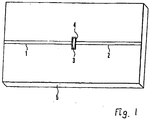
- Fig. 1 illustrates the use of a PEN waveplate of the present invention,
- Fig. 2 is a diagram illustrating a the loss as a function of gap width at 1550 nm,
- Fig. 3 illustrates the effect of draw ratio on the birefringence of PEN film,
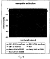
- Fig. 4 is a diagram showing extinction properties of a PEN waveplate, and
- Fig. 5 illustrates the use of a PEN waveplate in an arrayed waveguide grating.
-
- Polyethylene naphthalate (PEN) has the following chemical formula, somewhat similar to another popular polymer, polyethylene terephthalate:
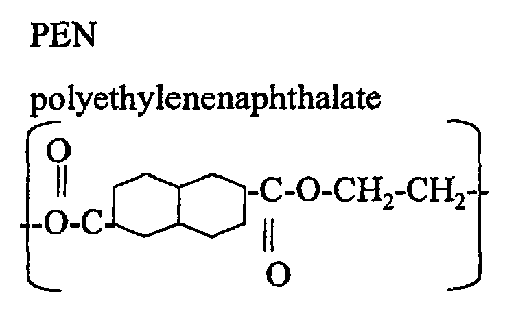

- Chemically, both these polymers are polyesters. An attractive property of these polymers is self-supporting thin film forming by means of extrusion. The thin film of PET is well known under the brand name (DuPont) of Mylar. The present work is only concerned with PEN films as its performance appears significantly higher than that of PET.
- PEN film is commercially produced by Teijin (Japan) under the trade name Teonex and DuPont (USA) under the trademark Kaladex. The basic properties of the polymer film are as follows:
- high in-plane birefringence (up to 0.3, obtained or promoted by stretching of a PEN sheet)
- relatively high glass transition temperature, Tg, 122° C
- high solvent resistivity
- relatively high mechanical strength, sufficient to enable the processing of thin sheets of the polymer.
- high extinction of an optical signal in specific conditions.
- To obtain a waveplate, the PEN material is extruded into a film. The extrusion process is followed by two-dimensional (biaxial) stretching, to bring the thickness to the desired value and to enhance the in-plane mechanical properties. To bring the inplane birefringence to the desired level, an additional one-dimensional (uniaxial) stretching (post stretching) is applied.
- To rotate the polarization of a light beam by 90 degrees, half-wave retardation is needed. Hence, the product of thickness and birefringence of the retarder element must be half the wavelength used (usually, but not exclusively, around 1550 nm).
- To keep the optical losses by diffraction through the gap at a low level, the thickness of the waveplate should be smaller than about 20 microns, as seen in Fig. 2 representing the loss as a function of gap width at 1550 nm.
It follows that the birefringence of the waveplate material should be relatively large (min, approx. 0.04) to produce the retardation half wave. - The half wave retardation for 1550 nm (1.55µm) is 0.775 microns. It is possible to induce a birefringence up to about 0.35 in the PEN film. A realistic minimum thickness of the waveplate is therefore 0.775/0.35 = 2.2 µm. The maximum thickness of the waveplate is determined by acceptable diffraction losses. A
plate 20 µm thick yields 0.25 dB loss (Fig. 1) while a 25 µm plate yields as much as 0.4 dB. - Uniaxially stretched PEN foil exhibits in-plane birefringence due to the draw ratio. Fig.3 illustrates this relationship. It can be seen that a moderate draw ratio of, say, 50% already results in a birefringence of 0.05.
- Commercially available PEN foils are always stretched in two directions that are perpendicular to each other as the stretching brings about an improvement of mechanical properties in the direction of stretching of the foil. Biaxially stretched PEN foil as obtained from the manufacturer (Teijin) exhibits birefringence due to an unbalanced draw ratio.
- Commercially available Teijin PEN films (foil) may require a small amount of post- stretching to arrive at a birefringence that produces half-wave retardation. The need for the post-stretching and the amount thereof should be assessed individually on an as-needed basis.
- In a specific example, a waveplate material was obtained by post-stretching samples of a 16 µm Teijin Q51 film. A small stretching apparatus was built which consisted of a fixed clamp and a movable clamp on a rail. The foil samples were 25 mm in width and of various length up to 100 mm. The apparatus was placed in a tubular hot wall oven to stretch the foil at approx. the Tg temperature by pulling at the movable clamp.
- The draw ratios were from 2.5 % to more than 10 %. The samples after drawing were evaluated using visible light between crossed polarizers.
- The color of the central part of the sample changed as a result of the drawing as follows, starting from the original second order green:
Draw ratio (%) Color 2.5 second order yellow/orange 3.75 second order pale red 5 second order dark red 7.5 third order blue-green > 10 high-order pink - When passed through parallel polarizers with the waveplate in between, an optical signal undergoes an extinction that is very high when the waveplate retardation is exactly half wave, since the light polarized by the first polarizer is rotated by precisely 90° by the waveplate and is blocked by the second polarizer that is parallel to the first polarizer. Therefore, extinction induced by the halfwave plate between parallel polarizers is a way to assess the quality of the waveplate.
- The results of the PEN waveplates exceeded in certain respect the performance of corresponding NTT (polyimide) waveplates. For example, the 3.75% stretched Q51 16 □ m foil showed an extinction < - 30dB over the entire C band (1525-1565 nm) as shown in Fig. 4.
- In a specific use of the invention, as illustrated in Fig 1, a
PEN waveplate 3 of the invention, of the size approximately 2 mm x 5 mm and thickness of 16 µm was installed in a 20 µm wide slot 4 formed in the middle of an optical path of asingle silica waveguide 1, 2 having a cross-sectional width of 10 x 10 µm made in asilicon substrate 5. The waveplate was installed at an angle of about 85° to the optical axis of the waveguide to avoid back reflection. This angle can be selected in a range approximately 80-88°. - Alternatively, as shown in Fig. 5, the waveplate can be installed in an arrayed waveguide grating (AWG), where the
waveplate 3 is placed in a groove 4 cut acrosswaveguides 6 made in asilicon substrate 5. - Comparative tests were conducted of PEN HWPs with polyimide HWPs for 20 various chips. The chips used had ultra-high PDL and PDλ, and both the PEN and Polyimide HWPs showed a significant reduction of both respectively. These results support the conclusion that the PEN HWPs are a low-cost alternative to the polyimide HWPs without sacrificing optical performance.
- The results are displayed in the table:
BEFORE HWP AFTER HWP DIFF (B-A) DIFF (B-A) Device Ave PDL Ave PDLambda Ave PDL all chs Ave PDLambda all chs Nortel all chs Nortel Act. Center all chs PDL Diff. PDLambda Diff. ± 100(pm) BW 3dBGeneral (pm) ± 100(pm) BW 3dBGeneral (pm) IN22 Rigtailed E84 0.39 19.06 0.18 1.08 0.21 17.98 E111 0.24 18.07 0.25 16.64 -0.01 1.43 E349_8 0.50 22.31 0.34 3.49 0.16 18.82 E349_12 0.41 16.16 0.48 33.22 -0.07 -17.06 E349_16 0.26 5.72 0.21 8.67 0.04 -2.94 Average 0.36 16.26 0.30 12.62 0.07 3.64 IN22 Screened E40 UV no data 0.51 17.58 E68 UV 0.40 13.06 0.17 4.15 0.23 8.91 E81 UV no data 0.31 12.64 E101 UV no data 0.61 38.97 E103 UV 0.21 97.35 0.89 22.05 -0.68 75.30 E176 UV no data 0.74 17.85 E39 no data 0.48 30.84 E82 no data 0.51 19.10 E97 no data 0.56 31.23 E100 no data 0.34 1.66 E104 no data 0.38 21.14 E113 no data 0.37 11.35 E177 no data 0.45 6.26 Average 0.49 18.06 Device Ave PDL all chs Ave PDLambda Ave PDL all chs Ave PDLambda Ave PDL all chs Ave PDLambda Act. Center all chs Act. Center all chs Act. Center all chs ± 100(pm) BW 3dBGeneral (pm) ± 100(pm) BW 3dBGeneral (pm) ± 100(pm) BW 3dBGeneral (pm) IN22 Screened E417 0.22 3.45 0.80 2.32 -0.58 1.13 E420 0.31 3.28 0.19 6.86 0.12 -3.58 E422 0.46 11.56 0.27 6.76 0.19 4.80 E424 0.40 2.46 0.54 5.37 -0.14 -2.91 E426 0.37 4.81 0.26 3.78 0.10 1.03 E430 0.32 3.32 0.46 5.16 -0.15 -1.84 Average 0.35 4.81 0.42 5.04 -0.08 -0.23 - It can be seen that the waveplates of the invention are quite effective in alleviating the problem of polarization dependence of planar lightwave circuits such as AWGs.
- An advantage of the PEN waveplates over the PI waveplates is their uniformity over large area owing to the large size extrusion process of PEN films. The PI films, described in the Ando US patent, supra, are made by a spin coating and release Silicon onto wafers and yield much smaller size waveplates. It is conceivable to provide a wafer sized PEN waveplate, with a length approximately 20 mm thus covering a large number of waveguide channels across the width of an optical wafer. In this manner, a large number of components can be equipped with a waveplate using a slot that runs across the entire wafer. This of course is a cost-effective measure, both from the material and labor standpoint.
- In summary, PEN waveplates represent a technically and commercially viable solution to the polarization dependence problem of PLCs.
Claims (9)
- An optical waveplate comprising polyethylene naphthalate.
- The optical waveplate of claim 1 in the form of a film with a thickness in the range of 2 to about 25 µm.
- The optical waveplate of claim 2 wherein the film is an uniaxially stretched film.
- The optical waveplate of claim 2 wherein the film is a biaxially stretched film.
- An optical device comprisingat least an optical waveguide having each at least two sections, anda polyethylene naphthalate optical waveplate optically coupled between two sections of the waveguide to transmit a light signal between said two sections of the waveguide.
- The optical device of claim 4 wherein the waveplate has a thickness in the range of 2 to about 25 µm.
- The optical device of claim 4 wherein the waveguide defines an optical axis and the waveplate is disposed at an angle in the range 80-88° to the optical axis of the waveguide.
- The optical device of claim 4 wherein the waveguide is an arrayed waveguide grating.
- The optical device comprisinga wafer,a plurality of waveguides extending across the wafer,a slot extending across the waveguides, anda polyethylene naphthalate optical waveplate disposed in the slot and extending therealong so as to optically modify optical signals passing through the waveguides.
Applications Claiming Priority (2)
| Application Number | Priority Date | Filing Date | Title |
|---|---|---|---|
| CA002315997A CA2315997A1 (en) | 2000-08-15 | 2000-08-15 | Waveplates from pen |
| CA2315997 | 2000-08-15 |
Publications (1)
| Publication Number | Publication Date |
|---|---|
| EP1191363A1 true EP1191363A1 (en) | 2002-03-27 |
Family
ID=4166895
Family Applications (1)
| Application Number | Title | Priority Date | Filing Date |
|---|---|---|---|
| EP01306797A Withdrawn EP1191363A1 (en) | 2000-08-15 | 2001-08-09 | Optical waveplate and optical device using the waveplate |
Country Status (5)
| Country | Link |
|---|---|
| US (1) | US6757472B2 (en) |
| EP (1) | EP1191363A1 (en) |
| JP (1) | JP2002139627A (en) |
| CN (1) | CN1195237C (en) |
| CA (1) | CA2315997A1 (en) |
Cited By (2)
| Publication number | Priority date | Publication date | Assignee | Title |
|---|---|---|---|---|
| WO2018146221A1 (en) * | 2017-02-08 | 2018-08-16 | Rockley Photonics Limited | T-shaped arrayed waveguide grating |
| US11733461B2 (en) | 2017-07-17 | 2023-08-22 | Rockley Photonics Limited | Athermalized multi-path interference filter |
Families Citing this family (3)
| Publication number | Priority date | Publication date | Assignee | Title |
|---|---|---|---|---|
| US20040193691A1 (en) * | 2003-03-31 | 2004-09-30 | Chang William I. | System and method for providing an open eMail directory |
| JP4682111B2 (en) * | 2006-09-14 | 2011-05-11 | 富士通株式会社 | Waveguide type optical device and manufacturing method thereof |
| FI129636B (en) * | 2019-05-03 | 2022-06-15 | Teknologian Tutkimuskeskus Vtt Oy | Polarization rotator |
Citations (2)
| Publication number | Priority date | Publication date | Assignee | Title |
|---|---|---|---|---|
| US4756953A (en) * | 1985-12-09 | 1988-07-12 | Diafoil Company, Limited | Uniaxially high-oriented polyethylene naphthalate film for polarizing plates |
| US5901259A (en) * | 1993-05-07 | 1999-05-04 | Nippon Telegraph And Telephone Corporation | Optical waveplate, method of manufacturing the same, and waveguide device using the same |
Family Cites Families (1)
| Publication number | Priority date | Publication date | Assignee | Title |
|---|---|---|---|---|
| US5903392A (en) * | 1997-05-19 | 1999-05-11 | Dai Nippon Printing Co., Ltd. | Reflecting screen |
-
2000
- 2000-08-15 CA CA002315997A patent/CA2315997A1/en not_active Abandoned
-
2001
- 2001-08-09 US US09/924,578 patent/US6757472B2/en not_active Expired - Lifetime
- 2001-08-09 EP EP01306797A patent/EP1191363A1/en not_active Withdrawn
- 2001-08-15 JP JP2001246384A patent/JP2002139627A/en not_active Withdrawn
- 2001-08-15 CN CNB011331496A patent/CN1195237C/en not_active Expired - Fee Related
Patent Citations (2)
| Publication number | Priority date | Publication date | Assignee | Title |
|---|---|---|---|---|
| US4756953A (en) * | 1985-12-09 | 1988-07-12 | Diafoil Company, Limited | Uniaxially high-oriented polyethylene naphthalate film for polarizing plates |
| US5901259A (en) * | 1993-05-07 | 1999-05-04 | Nippon Telegraph And Telephone Corporation | Optical waveplate, method of manufacturing the same, and waveguide device using the same |
Cited By (5)
| Publication number | Priority date | Publication date | Assignee | Title |
|---|---|---|---|---|
| WO2018146221A1 (en) * | 2017-02-08 | 2018-08-16 | Rockley Photonics Limited | T-shaped arrayed waveguide grating |
| US10488589B2 (en) | 2017-02-08 | 2019-11-26 | Rockley Photonics Limited | T-shaped arrayed waveguide grating |
| US10955613B2 (en) | 2017-02-08 | 2021-03-23 | Rockley Photonics Limited | Arrayed waveguide grating with free propagation region matching |
| US11119273B2 (en) | 2017-02-08 | 2021-09-14 | Rockley Photonics Limited | T-shaped arrayed waveguide grating |
| US11733461B2 (en) | 2017-07-17 | 2023-08-22 | Rockley Photonics Limited | Athermalized multi-path interference filter |
Also Published As
| Publication number | Publication date |
|---|---|
| US6757472B2 (en) | 2004-06-29 |
| US20020044744A1 (en) | 2002-04-18 |
| JP2002139627A (en) | 2002-05-17 |
| CA2315997A1 (en) | 2002-02-15 |
| CN1195237C (en) | 2005-03-30 |
| CN1338648A (en) | 2002-03-06 |
Similar Documents
| Publication | Publication Date | Title |
|---|---|---|
| EP0890120B1 (en) | Nonpolarizing beamsplitter | |
| JP3621415B2 (en) | Light transmissive liquid crystal display | |
| JP6373625B2 (en) | Inverse wavelength dispersion phase retardation film and display device including the same | |
| KR101971754B1 (en) | Apodized broadband partial reflectors having differing optical packets | |
| KR102768152B1 (en) | Optically anisotropic laminate, polarizing plate, and image display device | |
| CA2208234A1 (en) | Multilayered optical film | |
| TWI224690B (en) | Optical wave guide coupled circuit device | |
| EP1191363A1 (en) | Optical waveplate and optical device using the waveplate | |
| JP4746475B2 (en) | Reflective polarizing plate | |
| EP1232413B1 (en) | Optical circuit element and method of producing the same | |
| US6421176B1 (en) | Optical isolator | |
| KR20200042411A (en) | Polarizing plate with retardation layer and image display device using the same | |
| EP1112528B1 (en) | Optical isolator | |
| CA2354907A1 (en) | Optical waveplate and an optical device using the waveplate | |
| KR100657725B1 (en) | Multilayer optical coating | |
| KR20250149965A (en) | Method for manufacturing optical film pieces and method for managing long-length optical films | |
| CN120641799A (en) | Display system manufacturing method and optical film assembly | |
| JP2002243960A (en) | Filter type multi-channel polymer wavelength multiplexer / demultiplexer | |
| JP2000155289A (en) | Optical isolator | |
| CN118786381A (en) | Display system, optical laminate, and method for manufacturing display system | |
| KR20240157667A (en) | Display system, optical laminate and method for manufacturing display system | |
| KR20240155243A (en) | Lens, display body and display method | |
| KR20240155242A (en) | Lens, display body and display method | |
| CN120836002A (en) | Lens unit, display body, and display method | |
| CA2261447A1 (en) | High isolation optical switch, isolator or circulator having thin film polarizing beam-splitters |
Legal Events
| Date | Code | Title | Description |
|---|---|---|---|
| PUAI | Public reference made under article 153(3) epc to a published international application that has entered the european phase |
Free format text: ORIGINAL CODE: 0009012 |
|
| AK | Designated contracting states |
Kind code of ref document: A1 Designated state(s): AT BE CH CY DE DK ES FI FR GB GR IE IT LI LU MC NL PT SE TR |
|
| AX | Request for extension of the european patent |
Free format text: AL;LT;LV;MK;RO;SI |
|
| AKX | Designation fees paid | ||
| 17P | Request for examination filed |
Effective date: 20021126 |
|
| RBV | Designated contracting states (corrected) |
Designated state(s): DE FR GB NL |
|
| 17Q | First examination report despatched |
Effective date: 20041019 |
|
| 17Q | First examination report despatched |
Effective date: 20041019 |
|
| STAA | Information on the status of an ep patent application or granted ep patent |
Free format text: STATUS: THE APPLICATION IS DEEMED TO BE WITHDRAWN |
|
| 18D | Application deemed to be withdrawn |
Effective date: 20100301 |