EP1191361A1 - Heater module for optical waveguide device - Google Patents
Heater module for optical waveguide device Download PDFInfo
- Publication number
- EP1191361A1 EP1191361A1 EP01308094A EP01308094A EP1191361A1 EP 1191361 A1 EP1191361 A1 EP 1191361A1 EP 01308094 A EP01308094 A EP 01308094A EP 01308094 A EP01308094 A EP 01308094A EP 1191361 A1 EP1191361 A1 EP 1191361A1
- Authority
- EP
- European Patent Office
- Prior art keywords
- optical waveguide
- waveguide device
- heat
- recessed groove
- groove portion
- Prior art date
- Legal status (The legal status is an assumption and is not a legal conclusion. Google has not performed a legal analysis and makes no representation as to the accuracy of the status listed.)
- Granted
Links
Images


Classifications
-
- G—PHYSICS
- G02—OPTICS
- G02B—OPTICAL ELEMENTS, SYSTEMS OR APPARATUS
- G02B6/00—Light guides; Structural details of arrangements comprising light guides and other optical elements, e.g. couplings
- G02B6/24—Coupling light guides
- G02B6/42—Coupling light guides with opto-electronic elements
-
- H—ELECTRICITY
- H01—ELECTRIC ELEMENTS
- H01L—SEMICONDUCTOR DEVICES NOT COVERED BY CLASS H10
- H01L21/00—Processes or apparatus adapted for the manufacture or treatment of semiconductor or solid state devices or of parts thereof
- H01L21/67—Apparatus specially adapted for handling semiconductor or electric solid state devices during manufacture or treatment thereof; Apparatus specially adapted for handling wafers during manufacture or treatment of semiconductor or electric solid state devices or components ; Apparatus not specifically provided for elsewhere
- H01L21/67005—Apparatus not specifically provided for elsewhere
- H01L21/67011—Apparatus for manufacture or treatment
- H01L21/67098—Apparatus for thermal treatment
- H01L21/67103—Apparatus for thermal treatment mainly by conduction
-
- G—PHYSICS
- G02—OPTICS
- G02B—OPTICAL ELEMENTS, SYSTEMS OR APPARATUS
- G02B6/00—Light guides; Structural details of arrangements comprising light guides and other optical elements, e.g. couplings
- G02B6/24—Coupling light guides
- G02B6/26—Optical coupling means
- G02B6/30—Optical coupling means for use between fibre and thin-film device
-
- H—ELECTRICITY
- H01—ELECTRIC ELEMENTS
- H01L—SEMICONDUCTOR DEVICES NOT COVERED BY CLASS H10
- H01L23/00—Details of semiconductor or other solid state devices
- H01L23/34—Arrangements for cooling, heating, ventilating or temperature compensation ; Temperature sensing arrangements
- H01L23/345—Arrangements for heating
-
- H—ELECTRICITY
- H01—ELECTRIC ELEMENTS
- H01L—SEMICONDUCTOR DEVICES NOT COVERED BY CLASS H10
- H01L2924/00—Indexing scheme for arrangements or methods for connecting or disconnecting semiconductor or solid-state bodies as covered by H01L24/00
- H01L2924/0001—Technical content checked by a classifier
- H01L2924/0002—Not covered by any one of groups H01L24/00, H01L24/00 and H01L2224/00
Landscapes
- Physics & Mathematics (AREA)
- General Physics & Mathematics (AREA)
- Engineering & Computer Science (AREA)
- Condensed Matter Physics & Semiconductors (AREA)
- Computer Hardware Design (AREA)
- Microelectronics & Electronic Packaging (AREA)
- Power Engineering (AREA)
- Optics & Photonics (AREA)
- Manufacturing & Machinery (AREA)
- Optical Integrated Circuits (AREA)
Abstract
A heater module (20) in accordance with the present invention is a heater module (20) for heating an optical waveguide device (12) so as to regulate its temperature; and comprises a heat-generating circuit adapted to generate heat when energized, and a heat-transmitting section disposed on the upper face of the heat-generating circuit and formed with a recessed groove portion for mounting the optical waveguide device (12).
When the optical waveguide device (12) is mounted on the bottom face of the heat-transmitting section (21) formed with the recessed groove section, the optical waveguide device (12) can be heated not only from its bottom face, but also from its side faces by edge parts constituting the recessed groove portion, whereby the temperature uniformity can be enhanced.
Description
- The present invention relates to a heater module for heating an optical waveguide device so as to regulate the temperature of the optical waveguide device, and an optical waveguide device equipped with the same.
- If an optical waveguide module has a large temperature distribution within an optical waveguide device, the size of the optical waveguide will vary due to differences in thermal expansion of its substrate depending on locations, thereby damaging its wavelength selectivity and switching characteristics. Therefore, an uniformity in temperature is required within the optical waveguide device.
- As a device for regulating the temperature of optical waveguide devices, thermoelectric cooling module and heaters have conventionally been utilized. Since it is necessary for an optical waveguide module to draw thereinto an optical fiber used for transmitting optical signals with respect to external devices, hermetic sealing is difficult at the drawing portion. Therefore, it is impossible for thermoelectric cooling module to secure their reliability, whereby heaters are often used as a temperature-regulating device. Inaheater, a heat-generating circuit (resistance) adapted to generate heat when energized is provided within an insulating layer, whereby the heat from the heat-generating circuit is transmitted to the optical waveguide device by way of the insulating layer.
- Conventionally, ceramics heaters made of alumina having a relatively low thermal conductivity (thermal conductivity of 20 W/mK) and the like have often been used. However, tendencies toward larger capacities and higher-speed communications have nowadays become remarkable, in particular, in the field of optical communications. Recently, along with the shift to D-WDM (Dense Wavelength Division Multiplexing), optical waveguide devices having large areas have come into use. Further, there has been an increasing demand for multiplexing a greater number of signals than those conventionally multiplexed for a certain frequency width, thereby enhancing the demand for uniformity in temperature. Hence, it is desired that the uniformity in temperature within the optical waveguide device be further improved (to become ±0.5°C or less).
- In order to satisfy such a demand for uniformity in temperature of the optical waveguide device, two methods have currently been under consideration. The first method is one using a heat spreader employing a Cu alloy or the like having a favorable thermal conductivity. It is a method in which the heat generated by an alumina heater is once uniformly dispersed by the heat spreader and then is transmitted to the optical waveguide device, so as to improve the uniformity in temperature. The second method is one in which the heater itself is formed from AlN or the like having a thermal conductivity (thermal conductivity of 170 W/mK) which is about 10 times that of conventionally used alumina, so that the heat generated by the heater is uniformly dispersed by the heater itself and then is transmitted to the optical waveguide device, whereby the uniformity in temperature is improved. When these methods are employed, the temperature distribution of the optical waveguide device can be made ±0.5°C or less.
- However, demands for D-WDM have recently been becoming severer in a drastic manner, whereby further multiplexing is desired. As a consequence, a temperature uniformity higher than that conventionally achieved is required for optical waveguide devices. Further, photonic networks making full use of optical switching and the like without using electric devices at all have been under consideration. For realizing them, devices using newmaterials such as LiNbO3 and resin waveguides, which are different from conventional quartz and silica, have been under consideration as optical waveguide devices. For these devices, a temperature uniformity severer than that conventionally demanded is required, and there is a case where a temperature uniformity of ±0.1°C or less is required for an optical waveguide device.
- In order to overcome such problems, as shown in Fig. 7, an attempt to realize a temperature uniformity of ±0.1°C or less was carried out by utilizing the fact that the temperature uniformity of an
optical waveguide device 71 improves when the thickness of aceramics heater 73 or the thickness of aheat spreader 72 is enhanced. In this case, though the temperature uniformity in theoptical waveguide device 71 was maintained in its surface bonded to theceramics heater 73 orheat spreader 72, the surface opposite from the one bonded to theceramics heater 73 orheat spreader 72 was exposed to an ambient temperature, whereby theoptical waveguide device 71 was cooled, thus failing to realize a temperature uniformity of ±0.1°C or less. - In order to prevent the upper part of the
optical waveguide device 71 frombeing cooled, there maybe considered a method in which theoptical waveguide device 71 is heated by a heater from both upper and lower faces of theoptical waveguide device 71, or a method in which the heater for heating is not constituted by ceramics but by asilicone 74 or polyimide heater, which can be bent freely as shown in Fig. 8, and the heater is processed into a tubular form having a center part at which theoptical waveguide device 71 is installed. - However, the above-mentioned methods heat not only the
optical waveguide device 71 but also the whole optical module, thereby being problematic in that the power consumption increases to about two times or more that in the case where heating is effected from only the lower face of theoptical waveguide device 71. Also, they are problematic in that the optical waveguide module inevitably increases its thickness. While an optical waveguide module is required to have a thickness of about 10 mm, which is typical as a module other than the optical waveguide module, the thickness of the optical waveguide module becomes about 20 to 30 mm in the above-mentioned methods. Therefore, in an apparatus equipped with the optical waveguide module, design rules for designing an apparatus constituted by other devices alone are not applicable, so that a special design is necessary, whereby not only the efficiency in designing and the cost of design, but also the cost of the whole apparatus increases. - Therefore, it is an object of the present invention to provide a heater module which can improve the temperature uniformity in an optical waveguide while keeping the power consumption and the thickness of the optical waveguide module by overcoming the problems mentioned above, and an optical waveguide module equipped therewith.
- The heater module in accordance with the present invention is a heater module for heating an optical waveguide device so as to regulate a temperature of the optical waveguide device, the heater module comprising a heat-generating circuit adapted to generate heat when energized; and a heat-transmitting section disposed on an upper face of the heat-generating circuit and formed with a recessed groove portion for mounting the optical waveguide device.
- In the present invention, the heat-transmitting section for heating an optical waveguide device is formed with a recessed groove portion, and the optical waveguide device is mounted in this recessed groove portion. The inventors have found that such a configuration makes it possible to heat the optical waveguide device not only from its bottom face but also from its side faces by way of edge parts constituting the recessed groove portion, whereby the temperature uniformity can be enhanced. Since the heat is transmitted from the edge parts of the recessed groove portion formed in the integral heat-transmitting section in the configuration of the present invention, it is not necessary to provide
respective heaters 75 for generating heat at the bottom and side faces as shown in Fig. 9. Also, since the optical waveguide device can be mounted so as to be inserted into the recessed groove portion formed in the heat-transmitting section, no heat-transmitting section for heating the upper face of the optical waveguide device is necessary, whereby a simple configuration can realize a heater module capable of enhancing the temperature uniformity. As a consequence, the thickness of the optical waveguide module using the optical waveguide device can be kept on a par with that in the case where the optical waveguide device is simply mounted on the heat-transmitting section. - In the heater module, the heat-transmitting section may be constituted by AlN ceramics.
- When the heat-transmitting section is thus constituted by AlN ceramics having a high thermal conductivity, the temperature uniformity of the heated optical waveguide device can further be enhanced.
- Preferably, in the heater module, an insulating layer is disposed between the heating circuit and the heat-transmitting section.
- The optical waveguide module in accordance with the present invention comprises the above-mentioned heater module, an optical waveguide device mounted in a recessed groove portion formed in the heat-transmitting section, and a housing accommodating the heater module and the optical waveguide device.
- When an optical waveguide module for heating an optical waveguide device is constituted by using the above-mentioned heater module as such, the temperature uniformity of the optical waveguide device can be enhanced, and the optical waveguide module can be realized by a simple configuration, whereby the thickness of the optical waveguide module can be kept on a par with that in the case where the optical waveguide device is simply mounted on the heat-transmitting section.
- Preferably, a gaseous medium is interposed in a space defined between an edge part of the recessed groove portion and the optical waveguide device, and the upper face of the edge part constituting the recessed groove portion is higher than the upper face of the optical waveguide device mounted on the bottom face of the recessed groove portion, or has a level difference not greater than 0.1 mm with respect to the upper face of the optical waveguide device or not greater than 1/10 of the height of the optical waveguide device.
- The edge part of the recessed groove portion acts to transmit the heat, which is transmitted to the heat-transmitting section, to the optical waveguide device. The heat from the edge part is transmitted by way of the gaseous medium interposed between the optical waveguide device and the edge part. When the upper face of the edge part is lower than the upper face of the optical waveguide device, the heat is transmitted to the optical waveguide device up to the height of the upper face of the edge part but not to its portion higher than the edge part. In this case, the upper face of the optical waveguide device is cooled by the ambient temperature. As a result of simulations of the relationship between the height of the edge part and the temperature uniformity, it has been found that, in the case where the upper face of the edge part is higher than the upper face of the optical waveguide device or where the upper face of the optical waveguide device is higher than the edge part, a desirable temperature uniformity (±0.1°C or less) can be realized when their difference is not greater than 0.1 mm or not greater than 1/10 of the height of the optical waveguide device.
- Preferably, a gaseous medium is interposed in a space defined between an edge part of the recessed groove portion and the optical waveguide device, and the space defined between the edge part of the recessed groove portion and the optical waveguide device has a width of at least 0.02 mm but not greater than 1.0 mm.
- If the width of the space between the edge part and the heat-transmitting section is shorter than 0.02 mm, a portion where the heat-transmitting section and the optical waveguide device partly come into contact with each other will occur due to problems in the processing accuracy of the heat-transmitting section, whereby the temperature uniformity of the optical waveguide device cannot be secured. If the width of the space between the edge part and the heat-transmitting section is greater than 1.0 mm, heat cannot efficiently be transmitted to side faces of the optical waveguide device when convection occurs within the optical waveguide module due to partial temperature differences and the like, whereby the temperature uniformity cannot be secured. Therefore, it is preferred that the width of the space between the edge part and the heat-transmitting section be at least 0.02 mm but not greater than 1.0 mm. Further, according to the structure of the optical waveguide module, it is desirable that the width of the space be 0.5 mm or less in order to keep the convection from influencing the space.
- The optical waveguide module may further comprise a resin interposed in a space defined between the edge part and the optical waveguide device.
- When a resin is interposed in a space defined between the edge part and the optical waveguide device as such, the resin can transmit heat from the heat-transmitting section to the optical waveguide device.
- In the optical waveguide module, the resin may be composed of a grease-like material.
- When a grease-like resin is used as such, no thermal stress acts on side faces of the optical waveguide device. Therefore, even when an optical waveguide susceptible to stress is used, the danger of damaging the optical waveguide device can be lowered.
- Fig. 1 is an exploded perspective view showing the optical waveguide module in accordance with a first embodiment.
- Fig. 2 is a sectional view showing the optical waveguide module in accordance with the first embodiment.
- Fig. 3 is a sectional view showing the optical waveguide module in accordance with the first embodiment.
- Fig. 4 is an explanatory view for explaining the housing of the optical waveguide module.
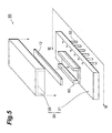
- Fig. 5 is an exploded perspective view showing the optical waveguide module in accordance with a second embodiment.
- Fig. 6 is a sectional view showing the optical waveguide module in accordance with the second embodiment.
- Fig. 7 is a view showing a conventional heater module.
- Fig. 8 is a view showing a conventional heater module.
- Fig. 9 is a view showing a conventional heater module.
- Preferred embodiments of the optical waveguide module in accordance with the present invention will now be explained in detail with reference to the drawings. In the explanation of the drawings, constituents identical to each other will be referred to with numerals identical to each other without repeating their overlapping descriptions.
- Fig. 1 is a perspective view showing the configuration of an
optical waveguide module 10 in accordance with a first embodiment, Fig. 2 is a sectional view of theoptical waveguide module 10 taken along the II-II direction, Fig. 3 is a sectional view of theoptical waveguide module 10 taken along the III-III direction, and Fig. 4 is an explanatory view for explaining ahousing 30. Theoptical waveguide module 10 comprises anoptical waveguide device 12 made of quartz with dimensions of 50 x 10 x 1 mm, aheater module 20 for heating theoptical waveguide device 12, and thehousing 30 for accommodating theoptical waveguide device 12 andheater module 20. - As shown in Fig. 2, the
heater module 20 is constituted by a heat-generatingcircuit 22, adapted to generate heat when energized, having a resistance of 0.5 to 10 Ω; and a heat-transmittingsection 21 disposed on the upper face of the heat-generatingcircuit 22. The heat-generatingcircuit 22 is formed from tungsten, molybdenum, silver-palladium, or the like, andelectrodes 23 for supplying an electric current to flow through the heat-generatingcircuit 22 are disposed at both ends of the heat-generatingcircuit 22. The heat-transmittingsection 21 disposed on the upper face of the heat-generatingcircuit 22 is formed by anAlN ceramics layer 21 having a high thermal conductivity. As shown in Fig. 3, the heat-transmittingsection 21 is formed with a recessed groove portion, and theoptical waveguide device 12 is mounted on thebottom face 21b of the recessed groove portion so as to be held betweenedge parts 21a constituting the recessed groove portion. Aresin 41 fills the gap between the mountedoptical waveguide device 12 and thebottom face 21b of the recessed groove portion, and the gap between theoptical waveguide device 12 and eachedge part 21a. The heat transmitted from the heat-generatingcircuit 22 is substantially uniformly dispersedwithintheAlNceramics layer 21. As a consequence, the heat is transmitted from thebottom face 21b andedge parts 21a of the recessed groove portion by way of theresin 41, so that theoptical waveguide device 12 mounted on the upper face of theAlN ceramics layer 21 is uniformly heated, whereby the temperature uniformity in theoptical waveguide device 12 can be enhanced. Also, since AlN ceramics are highly resistant to humidity, the resistance value of the heat-generatingcircuit 22 does not change even when continuously used for a long period of time, whereby a high reliability is obtained. Here, a method of making theheater module 20 will be explained. First, with W paste, the heat-generatingcircuit 22 and theelectrodes 23 are printed onapreformsheetofAlNceramics. Subsequently, thepreform sheet of AlN ceramics is applied to the upper face of the heat-generatingcircuit 22, so as to make a temporarily formed article of theheater module 20. This temporarily formed article is sintered in a nitrogen atmosphere of 1700°C or higher, so that the recessed groove portion is formed in the AlN ceramics, whereby theheater module 20 is accomplished. When mounting theoptical waveguide device 12 in theheater module 20, the amount of resin used for bonding theoptical waveguide device 12 and the recessed grooveportion bottom face 21b to each other is set greater, for example, so that theresin 41 spills over when theoptical waveguide device 12 and the heat-transmittingsection 21 are bonded to each other, and thus spilledresin 41 is used for filling the spaces between theoptical waveguide device 12 and theedge parts 21a of the recessed groove portion. Though theresin 41 used in this embodiment is a silicone resin, an epoxy resin can be used as well. Further, in order to lower the stress acting on theoptical waveguide device 12, a part of theresin 41 may be substituted by grease, for example, such that a part contacting to side faces of theoptical waveguide device 12 is a grease-like resin. - The
housing 30 is constituted by apackage substrate 31, to which lead pins 32 for energizing the heat-generatingcircuit 22 are soldered, for supporting theheater module 20; and acover 35 for covering the package substrate 31 (see Fig. 1). The whole package has dimensions of 100 x 50 x 10 mm. As shown in Fig. 4, two opposing faces of thecover 35 for thehousing 30 are formed withinsertion ports 35a for inserting anoptical fiber 14. Thepackage substrate 31 has aflat sheet 31a to which the lead pins 32 are soldered, andsupport sheets 31b bonded to both ends of the lower side of theflat sheet 31a (see Fig. 2). When thesupport sheets 31b are provided as such, excessive loads can be prevented from being exerted on the lead pins 32 when assembling theoptical waveguide module 10 into a system board and the like. Thecover 35 and thepackage substrate 31 are bonded to each other by a resin. Though the resin used in this embodiment is a silicone resin which is effective in preventing the deformation from occurring at the time of bonding, an epoxy resin can also be used. Thecover 35 and thepackage substrate 31 are mainly composed of copper-tungsten. Therefore, thehousing 30 has a high temperature uniformity, whereby the temperature uniformity in theoptical waveguide device 12 can be improved. Similar effects can also be obtained when thehousing 30 is mainly composed of cobalt, iron, nickel, alumina, or aluminum nitride. When thehousing 30 is mainly composed of a resin or silica glass, which is a highly heat-insulating material, the heat within thehousing 30 can be restrained from being emitted to the outside, whereby the temperature of theoptical waveguide device 12 can be prevented from decreasing. - In the
optical waveguide module 10 in accordance with this embodiment, the heat-transmittingsection 21 of the heater module for heating theoptical waveguide device 12 is formed with the recessed groove portion, in which theoptical waveguide device 12 is mounted. As a consequence, theoptical waveguide device 12 is heated from thebottom face 21b andedge parts 21a of the recessed groove portion, whereby the temperature uniformity in theoptical waveguide device 12 can be enhanced. When the temperature uniformity in theoptical waveguide device 12 was observed with a thermo-viewer under a condition in which the temperature of theheater module 20 was 80°C and the ambient temperature was 0°C, it was possible to hold the temperature distribution within ±0.1°C. As for the temperature controllability, only a change of ±0.2 or less in temperature was observed even when the ambient temperature was changed over the range of -40 to 70°C, whereby it was found to be less susceptible to the outside temperature. Also, theheater module 20 and theoptical waveguide device 12 were less likely to warp, no anisotropy was observed in optical waveguide characteristics, and no problems were found in the insertion loss, switching characteristics and dependence of polarization due to birefringence occurred. - Since a single heat-generating
circuit 22 can heat theoptical waveguide device 12 from theedge parts 21a andbottom face 21b, the optical module in accordance with this embodiment can improve the temperature uniformity while saving the power consumption. In an experiment carried out under the above-mentioned condition, the power consumption was 3 W or less. - An
optical waveguide module 50 in accordance with a second embodiment of the present invention will now be explained. Fig. 5 is a perspective view showing theoptical waveguide module 50 in accordance with the second embodiment, and Fig. 6 is a VI-VI sectional view of theoptical waveguide module 50. Theoptical waveguide module 50 in accordance with the second embodiment has a basic configuration identical to that of theoptical waveguide module 10 in accordance with the first embodiment but differs therefrom in the configuration of aheater module 60 for heating theoptical waveguide device 12. - As shown in Fig. 6, the
heater module 60 in the second embodiment has a heat-generatingcircuit 62 adapted to generate heat when energized, an insulatinglayer 61 disposed on the upper face of theheating circuit 62, and aheat spreader 65 disposed on the upper face of the insulatinglayer 61 by way of aresin 64. Theheating circuit 62 is formed from tungsten, molybdenum, silver-palladium, or the like, andelectrodes 63 for supplying an electric current to flow through the heat-generatingcircuit 62 are disposed at both ends of the heat-generatingcircuit 62. The insulatinglayer 61 disposed on the upper face of the heat-generatingcircuit 62 is made of alumina ceramics, and theheat spreader 65 disposed on the upper face of the insulatinglayer 61 is made of a Cu alloy. As shown in Fig. 5, theheat spreader 65 is formed with a recessed groove portion, and theoptical waveguide device 12 is mounted on the bottom face of the recessed groove portion so as to be held between edge parts constituting the recessed groove portion. The heat transmitted from the heat-generatingcircuit 62 is substantially uniformly dispersed within theheat spreader 65. As a consequence, to theoptical waveguide device 12 mounted on the upper face of theheat spreader 65, the heat is transmitted from its bottom face and edge parts, so that theoptical waveguide device 12 is uniformly heated, whereby its temperature uniformity can be enhanced. - As with the
optical waveguide module 10 in accordance with the first embodiment, theoptical waveguide module 50 having thus configuredheater module 60 is effective in enhancing the temperature uniformity in theoptical waveguide device 12. Though a ceramics heater in which the insulatinglayer 61 is made of alumina ceramics is used in this embodiment, other ceramics, e.g., AlN ceramics, may be used as well. Results substantially the same as those of theoptical waveguide module 50 in accordance with the second embodiment can also be obtained when silicone rubber or polyimide is used in place of ceramics. Further, theheat spreader 65 is not restricted to the Cu alloy, but may be a metal having a high thermal conductivity such as an Al alloy. - An optical waveguide module in accordance with a third embodiment of the present invention will now be explained. The optical waveguide module in accordance with the third embodiment has a basic configuration identical to that of the
optical waveguide module 50 in accordance with the second embodiment, but differs therefrom in that the space between theedge part 21a constituting the recessed groove portion and theoptical waveguide device 12 is filled with air instead of theresin 41. - Table 1 shows results of Experiment 1 in which the temperature uniformity in the optical waveguide device in thus configured optical waveguide module was measured while changing the width (corresponding to the width D shown in Fig. 3) of the space between the edge part of the recessed groove portion and the optical waveguide device. Here, the upper face of the optical waveguide device and the upper face of the
edge part 21a of the recessed groove portion are supposed to have the same height.The heat-transmitting section and the optical waveguide device have the same height. Space width (mm) Temperature uniformity (°C) Sample 1 0.01 ±0.2 Sample 2 0.02 ±0.1 Sample 3 0.1 ±0.07 Sample 4 0.5 ±0.09 Sample 5 1.0 ±0.1 Sample 6* 1.5 ±0.3 - As can be seen from this table, a temperature uniformity of ±0.1°C or less can be attained when the width of the space between the
edge part 21a of the recessed groove portion and the optical waveguide device is at least 0.02 mm but not greater than 1.0 mm. - Table 2 shows results of Experiment 2 in which the outside of the optical waveguide module in Experiment 1 was forcibly cooled with air at a wind speed of 5 m/s.
The heat-transmitting section and the optical waveguide device have the same height, with forcible cooling at a wind speed of 5 m/s. Space width (mm) Temperature uniformity (°C) Sample 7 0.01 ±0.2 Sample 8 0.02 ±0.1 Sample 9 0.1 ±0.07 Sample 100.5 ±0.09 Sample 11* 1.0 ±0.2 - As canbe seen from this table, a temperature uniformity of ±0.1°C or less can be attained when the width of the space between the
edge part 21a of the recessed groove portion and the optical waveguide device is at least 0.02 mm but not greater than 0.5 mm. - Table 3 shows results of Experiment 3 in which the temperature uniformity in the optical waveguide device in the optical waveguide module accordance with the third embodiment was measured while changing the height of the
edge part 21a of the recessed groove portion and the height of the optical waveguide device relative to each other. Here, the height of the optical waveguide device was set to 1.2 mm, and the width of the space between the optical waveguide device and theedge part 21a of the recessed groove portion was set to 0.1 mm.Space width = 0.1 mm, and the height of the optical waveguide device = 1.2 mm. Positional relationship between optical waveguide device and edge part (mm) Temperature uniformity (°C) Sample 120.01 ±0.07 Sample 13 0.05 ±0.07 Sample 140.12 ±0.1 Sample 15* 0.2 ±0.12 - As can be seen from this table, in the case where the optical waveguide device is higher than the
edge part 21a of the recessed groove portion, a temperature uniformity of ±0.1°C or less can be achieved when their difference is not greater than 0.1 mm, which is 1/10 of the thickness of the optical waveguide device. - Table 4 shows results of Experiment 4 in which the temperature uniformity in the optical waveguide device in the optical waveguide module in accordance with the third embodiment was measured while changing the height of the
edge part 21a of the recessed groove portion and the height of the optical waveguide device relative to each other. Here, the height of the optical waveguide device was set to 0.5 mm, and the width of the space between the optical waveguide device and theedge part 21a of the recessed groove portion was set to 0.1 mm.Space width = 0.1 mm, and the height of the optical waveguide device = 0.5 mm. Positional relationship between optical waveguide device and edge part (mm) Temperature uniformity (°C) Sample 16 0.01 ±0.06 Sample 17 0.05 ±0.06 Sample 18 0.1 ±0.08 Sample 19* 0.2 ±0.12 - As can be seen from this table, in the case where the optical waveguide device is higher than the
edge part 21a of the recessed groove portion, a temperature uniformity of ±0.1°C or less can be achieved when their difference is not greater than 0.1 mm, even if it is not 1/10 of the thickness of the optical waveguide device or less. - Table 5 shows results of Experiment 5 in which the height of the optical waveguide in Experiment 3 was made lower than that of the
edge part 21a of the recessed groove portion.Space width = 0.1 mm, and the height of the optical waveguide device = 1.2 mm. Positional relationship between optical waveguide device and edge part (mm) Temperature uniformity (°C) Sample 200.01 ±0.07 Sample 210.05 ±0.07 Sample 220.1 ±0.07 Sample 230.2 ±0.07 - As can be seen from this table, a temperature uniformity of ±0.1°C or less can be achieved when the
edge part 21a of the recessedgroove 21a is higher than the optical waveguide device. - Though embodiments of the present invention are explained in detail, the present invention is not restricted to the above-mentioned embodiments.
- Though the optical waveguide is made of quartz in the above-mentioned embodiment, it is not limited to one made of quartz. For example, optical waveguide devices made of resins, silica, LiNbO3, and the like may be used as well.
- Also, the dimensions of the optical waveguide device can be changed.
- Further, the resin used for bonding and the like, and the material used for the housing and the like are not limited to those in the above-mentioned embodiments.
- According to the present invention, a recessed groove portion is formed in the heat-transmitting section constituting the heater module, and the optical waveguide device is mounted so as to be inserted in the recessed groove portion, whereby the optical waveguide device is heated from the bottom face and side faces. Therefore, the temperature uniformity in the optical waveguide device can be improved.
- Also, since the present invention is not configured so as to heat the whole optical waveguide device, it can lower the power consumption for heating the optical waveguide device. Further, the thickness of the optical waveguide module can be kept on a par with that in the case where the optical waveguide device is simply mounted in the heat-transmitting section.
Claims (8)
- A heater module for heating an optical waveguide device so as to regulate a temperature of said optical waveguide device, said heater module comprising:a heat-generating circuit adapted to generate heat when energized; anda heat-transmitting section disposed on an upper face of said heat-generating circuit and formed with a recessed groove portion for mounting said optical waveguide device.
- A heater module according to claim 1, wherein said heat-transmitting section is constituted by AlN ceramics.
- A heater module according to claim 1 or 2, wherein an insulating layer is disposed between said heat-generating circuit and said heat-transmitting section.
- An optical waveguide module comprising:the heater module according to one of claims 1 to 3;an optical waveguide device mounted in a recessed groove portion formed in said heat-transmitting section; anda housing accommodating said heater module and said optical waveguide device.
- An optical waveguide module according to claim 4, wherein a gaseous medium is interposed in a space defined between an edge part of said recessed groove portion and said optical waveguide device; and
wherein an upper face of said edge part constituting said recessed groove portion is higher than an upper face of said optical waveguide device mounted on a bottom face of said recessed groove portion, or has a level difference not greater than 0.1 mm with respect to said upper face of said optical waveguide device or not greater than 1/10 of the height of said optical waveguide device. - An optical waveguide module according to claim 4, wherein a gaseous medium is interposed in a space defined between an edge part of said recessed groove portion and said optical waveguide device; and
wherein said space defined between said edge part of said recessed groove portion and said optical waveguide device has a width of at least 0.02 mm but not greater than 1.0 mm. - An optical waveguide module according to claim 4, further comprising a resin interposed in a space defined between said edge part and said optical waveguide device.
- An optical waveguide module according to claim 7, wherein said resin is composed of a grease-like material.
Applications Claiming Priority (2)
| Application Number | Priority Date | Filing Date | Title |
|---|---|---|---|
| JP2000290710 | 2000-09-25 | ||
| JP2000290710A JP2002098844A (en) | 2000-09-25 | 2000-09-25 | Heater module and optical waveguide module |
Publications (2)
| Publication Number | Publication Date |
|---|---|
| EP1191361A1 true EP1191361A1 (en) | 2002-03-27 |
| EP1191361B1 EP1191361B1 (en) | 2005-09-14 |
Family
ID=18773895
Family Applications (1)
| Application Number | Title | Priority Date | Filing Date |
|---|---|---|---|
| EP01308094A Expired - Lifetime EP1191361B1 (en) | 2000-09-25 | 2001-09-24 | Heater module for optical waveguide device |
Country Status (7)
| Country | Link |
|---|---|
| US (1) | US6618539B2 (en) |
| EP (1) | EP1191361B1 (en) |
| JP (1) | JP2002098844A (en) |
| KR (1) | KR20020024544A (en) |
| CA (1) | CA2357790C (en) |
| DE (1) | DE60113350T2 (en) |
| TW (1) | TW516335B (en) |
Cited By (3)
| Publication number | Priority date | Publication date | Assignee | Title |
|---|---|---|---|---|
| EP1526402A2 (en) | 2003-10-22 | 2005-04-27 | Fujitsu Limited | Optical device module |
| EP1526401A1 (en) * | 2003-10-22 | 2005-04-27 | Fujitsu Limited | Thermally controlled optical device module |
| EP2929765A4 (en) * | 2012-12-05 | 2016-07-20 | Ericsson Telefon Ab L M | System and method for regulating temperature of electronic component |
Families Citing this family (9)
| Publication number | Priority date | Publication date | Assignee | Title |
|---|---|---|---|---|
| US7085555B2 (en) | 2000-12-19 | 2006-08-01 | Bellsouth Intellectual Property Corporation | Location blocking service from a web advertiser |
| JP3667689B2 (en) * | 2001-12-10 | 2005-07-06 | 三菱電機株式会社 | Optical fiber holding device, optical dispersion equalizer, and manufacturing method of optical fiber holding device |
| JP2005316475A (en) * | 2004-04-29 | 2005-11-10 | Sumitomo Electric Ind Ltd | Optical transceiver |
| JP2012197978A (en) * | 2011-03-22 | 2012-10-18 | Toyota Industries Corp | Heat pump system |
| US9400402B2 (en) | 2014-01-07 | 2016-07-26 | Electronics And Telecommunications Research Institute | Optical waveguide and optical device based on the same |
| US9772664B1 (en) * | 2016-03-25 | 2017-09-26 | Adlink Technology Inc. | Memory heater and heating aid arrangement |
| US10502956B2 (en) * | 2017-06-27 | 2019-12-10 | Microsoft Technology Licensing, Llc | Systems and methods of reducing temperature gradients in optical waveguides |
| US20210349018A1 (en) * | 2020-05-07 | 2021-11-11 | Hand Held Products, Inc. | Apparatuses, systems, and methods for sample testing |
| US11846574B2 (en) | 2020-10-29 | 2023-12-19 | Hand Held Products, Inc. | Apparatuses, systems, and methods for sample capture and extraction |
Citations (7)
| Publication number | Priority date | Publication date | Assignee | Title |
|---|---|---|---|---|
| US3323886A (en) * | 1963-05-01 | 1967-06-06 | American Optical Corp | Radiation absorption heating of a bundle of glass fibers |
| US5288301A (en) * | 1989-09-01 | 1994-02-22 | Bt&D Technologies Limited | Method for fabrication of fused fibre devices |
| EP0603411A1 (en) * | 1992-07-01 | 1994-06-29 | KATOH, Keiichi | Ceramic heating/cooling device |
| EP0636909A1 (en) * | 1993-07-29 | 1995-02-01 | Sumitomo Electric Industries, Ltd. | Optical waveguide module |
| JPH07248425A (en) * | 1994-03-08 | 1995-09-26 | Sumitomo Electric Ind Ltd | Heater for reinforcing member of fusion spliced part of optical fibers |
| JPH10123340A (en) * | 1996-10-23 | 1998-05-15 | Hitachi Cable Ltd | Waveguide type optical module |
| US5818564A (en) * | 1996-09-13 | 1998-10-06 | Raychem Corporation | Assembly including an active matrix liquid crystal display module |
Family Cites Families (1)
| Publication number | Priority date | Publication date | Assignee | Title |
|---|---|---|---|---|
| JPH09211272A (en) * | 1996-01-31 | 1997-08-15 | Furukawa Electric Co Ltd:The | Optical module |
-
2000
- 2000-09-25 JP JP2000290710A patent/JP2002098844A/en active Pending
-
2001
- 2001-09-20 CA CA002357790A patent/CA2357790C/en not_active Expired - Fee Related
- 2001-09-24 US US09/961,191 patent/US6618539B2/en not_active Expired - Fee Related
- 2001-09-24 KR KR1020010058958A patent/KR20020024544A/en active IP Right Grant
- 2001-09-24 EP EP01308094A patent/EP1191361B1/en not_active Expired - Lifetime
- 2001-09-24 DE DE60113350T patent/DE60113350T2/en not_active Expired - Fee Related
- 2001-09-24 TW TW090123448A patent/TW516335B/en not_active IP Right Cessation
Patent Citations (7)
| Publication number | Priority date | Publication date | Assignee | Title |
|---|---|---|---|---|
| US3323886A (en) * | 1963-05-01 | 1967-06-06 | American Optical Corp | Radiation absorption heating of a bundle of glass fibers |
| US5288301A (en) * | 1989-09-01 | 1994-02-22 | Bt&D Technologies Limited | Method for fabrication of fused fibre devices |
| EP0603411A1 (en) * | 1992-07-01 | 1994-06-29 | KATOH, Keiichi | Ceramic heating/cooling device |
| EP0636909A1 (en) * | 1993-07-29 | 1995-02-01 | Sumitomo Electric Industries, Ltd. | Optical waveguide module |
| JPH07248425A (en) * | 1994-03-08 | 1995-09-26 | Sumitomo Electric Ind Ltd | Heater for reinforcing member of fusion spliced part of optical fibers |
| US5818564A (en) * | 1996-09-13 | 1998-10-06 | Raychem Corporation | Assembly including an active matrix liquid crystal display module |
| JPH10123340A (en) * | 1996-10-23 | 1998-05-15 | Hitachi Cable Ltd | Waveguide type optical module |
Non-Patent Citations (1)
| Title |
|---|
| TAKASUGI ET AL.: "Study on Reliability of Arrayed Waveguide Grating Modules", PROCEEDINGS OF THE GENERAL MEETING IN ELECTRONICS, THE INSITUTE OF ELECTRONICS, INFORMATION AND COMMUNICATION ENGINEERS, March 1999 (1999-03-01), pages 275, XP002945023 * |
Cited By (7)
| Publication number | Priority date | Publication date | Assignee | Title |
|---|---|---|---|---|
| EP1526402A2 (en) | 2003-10-22 | 2005-04-27 | Fujitsu Limited | Optical device module |
| EP1526401A1 (en) * | 2003-10-22 | 2005-04-27 | Fujitsu Limited | Thermally controlled optical device module |
| EP1526402A3 (en) * | 2003-10-22 | 2006-08-02 | Fujitsu Limited | Optical device module |
| EP1710615A1 (en) * | 2003-10-22 | 2006-10-11 | Fujitsu Limited | Thermally controlled optical device module |
| US7151866B2 (en) | 2003-10-22 | 2006-12-19 | Fujitsu Limited | Optical device module |
| US7476038B2 (en) | 2003-10-22 | 2009-01-13 | Fujitsu Limited | Optical device module |
| EP2929765A4 (en) * | 2012-12-05 | 2016-07-20 | Ericsson Telefon Ab L M | System and method for regulating temperature of electronic component |
Also Published As
| Publication number | Publication date |
|---|---|
| EP1191361B1 (en) | 2005-09-14 |
| US6618539B2 (en) | 2003-09-09 |
| KR20020024544A (en) | 2002-03-30 |
| TW516335B (en) | 2003-01-01 |
| CA2357790C (en) | 2005-05-24 |
| US20020057884A1 (en) | 2002-05-16 |
| DE60113350D1 (en) | 2005-10-20 |
| DE60113350T2 (en) | 2006-06-14 |
| JP2002098844A (en) | 2002-04-05 |
| CA2357790A1 (en) | 2002-03-25 |
Similar Documents
| Publication | Publication Date | Title |
|---|---|---|
| EP1191361B1 (en) | Heater module for optical waveguide device | |
| US4374316A (en) | Semiconductor integrated circuit supporter having a heating element | |
| EP0718934B1 (en) | Thermoelectric cooler assembly | |
| CN103370644B (en) | Optical circuit board | |
| EP0929206A2 (en) | Thermal housing for optical circuits | |
| KR20000006234A (en) | Stacked semiconductor device | |
| US20060049515A1 (en) | Memory module having memory chips protected from excessive heat | |
| EP2254206A1 (en) | Optical module | |
| EP1258752A1 (en) | Heater module and optical waveguide module | |
| CN110957278B (en) | Package for mounting electronic component and electronic device using the same | |
| US6740963B2 (en) | Optical module | |
| US8503181B2 (en) | Semiconductor device with a zigzag radiator | |
| US20030127445A1 (en) | Heater for heating waveguide and waveguide with heater | |
| US6583388B2 (en) | High thermal efficiency, small form-factor packages including thermally insulative cavities, and transfer molded variants | |
| JP2008197500A (en) | Optical module | |
| CN113376767A (en) | Chip packaging structure and optical computing device | |
| KR100416993B1 (en) | Optical element integrated heat transferring device for plc | |
| GB2536689A (en) | Carrier and insert | |
| JP3873096B2 (en) | Ceramic heating device | |
| US6600848B2 (en) | Integrated thermo-optical silica switch | |
| CN113620234B (en) | Chip packaging structure, control method and optical computing device | |
| JPH03118169A (en) | Holding device for led printer base | |
| JP2798656B2 (en) | Circuit board | |
| US20050141845A1 (en) | Temperature control element temperature control component, and waveguide opical module | |
| JP2000147277A (en) | Optical module |
Legal Events
| Date | Code | Title | Description |
|---|---|---|---|
| PUAI | Public reference made under article 153(3) epc to a published international application that has entered the european phase |
Free format text: ORIGINAL CODE: 0009012 |
|
| 17P | Request for examination filed |
Effective date: 20011009 |
|
| AK | Designated contracting states |
Kind code of ref document: A1 Designated state(s): AT BE CH CY DE DK ES FI FR GB GR IE IT LI LU MC NL PT SE TR |
|
| AX | Request for extension of the european patent |
Free format text: AL;LT;LV;MK;RO;SI |
|
| 17Q | First examination report despatched |
Effective date: 20020704 |
|
| AKX | Designation fees paid |
Free format text: DE FR GB IT |
|
| GRAP | Despatch of communication of intention to grant a patent |
Free format text: ORIGINAL CODE: EPIDOSNIGR1 |
|
| GRAS | Grant fee paid |
Free format text: ORIGINAL CODE: EPIDOSNIGR3 |
|
| GRAA | (expected) grant |
Free format text: ORIGINAL CODE: 0009210 |
|
| AK | Designated contracting states |
Kind code of ref document: B1 Designated state(s): DE FR GB IT |
|
| REG | Reference to a national code |
Ref country code: GB Ref legal event code: FG4D |
|
| REF | Corresponds to: |
Ref document number: 60113350 Country of ref document: DE Date of ref document: 20051020 Kind code of ref document: P |
|
| ET | Fr: translation filed | ||
| PLBE | No opposition filed within time limit |
Free format text: ORIGINAL CODE: 0009261 |
|
| STAA | Information on the status of an ep patent application or granted ep patent |
Free format text: STATUS: NO OPPOSITION FILED WITHIN TIME LIMIT |
|
| 26N | No opposition filed |
Effective date: 20060615 |
|
| PGFP | Annual fee paid to national office [announced via postgrant information from national office to epo] |
Ref country code: FR Payment date: 20080915 Year of fee payment: 8 |
|
| PGFP | Annual fee paid to national office [announced via postgrant information from national office to epo] |
Ref country code: GB Payment date: 20080924 Year of fee payment: 8 |
|
| PGFP | Annual fee paid to national office [announced via postgrant information from national office to epo] |
Ref country code: DE Payment date: 20081002 Year of fee payment: 8 |
|
| PGFP | Annual fee paid to national office [announced via postgrant information from national office to epo] |
Ref country code: IT Payment date: 20080927 Year of fee payment: 8 |
|
| GBPC | Gb: european patent ceased through non-payment of renewal fee |
Effective date: 20090924 |
|
| REG | Reference to a national code |
Ref country code: FR Ref legal event code: ST Effective date: 20100531 |
|
| PG25 | Lapsed in a contracting state [announced via postgrant information from national office to epo] |
Ref country code: DE Free format text: LAPSE BECAUSE OF NON-PAYMENT OF DUE FEES Effective date: 20100401 Ref country code: FR Free format text: LAPSE BECAUSE OF NON-PAYMENT OF DUE FEES Effective date: 20090930 |
|
| PG25 | Lapsed in a contracting state [announced via postgrant information from national office to epo] |
Ref country code: GB Free format text: LAPSE BECAUSE OF NON-PAYMENT OF DUE FEES Effective date: 20090924 |
|
| PG25 | Lapsed in a contracting state [announced via postgrant information from national office to epo] |
Ref country code: IT Free format text: LAPSE BECAUSE OF NON-PAYMENT OF DUE FEES Effective date: 20090924 |