EP1189491A1 - Apparatus for detecting plasma anomalous discharge and method of detecting the same - Google Patents
Apparatus for detecting plasma anomalous discharge and method of detecting the same Download PDFInfo
- Publication number
- EP1189491A1 EP1189491A1 EP01917520A EP01917520A EP1189491A1 EP 1189491 A1 EP1189491 A1 EP 1189491A1 EP 01917520 A EP01917520 A EP 01917520A EP 01917520 A EP01917520 A EP 01917520A EP 1189491 A1 EP1189491 A1 EP 1189491A1
- Authority
- EP
- European Patent Office
- Prior art keywords
- anomalous
- ultrasonic
- sensor
- source point
- plasma
- Prior art date
- Legal status (The legal status is an assumption and is not a legal conclusion. Google has not performed a legal analysis and makes no representation as to the accuracy of the status listed.)
- Withdrawn
Links
Images








Classifications
-
- G—PHYSICS
- G01—MEASURING; TESTING
- G01N—INVESTIGATING OR ANALYSING MATERIALS BY DETERMINING THEIR CHEMICAL OR PHYSICAL PROPERTIES
- G01N29/00—Investigating or analysing materials by the use of ultrasonic, sonic or infrasonic waves; Visualisation of the interior of objects by transmitting ultrasonic or sonic waves through the object
- G01N29/36—Detecting the response signal, e.g. electronic circuits specially adapted therefor
- G01N29/38—Detecting the response signal, e.g. electronic circuits specially adapted therefor by time filtering, e.g. using time gates
-
- B—PERFORMING OPERATIONS; TRANSPORTING
- B01—PHYSICAL OR CHEMICAL PROCESSES OR APPARATUS IN GENERAL
- B01J—CHEMICAL OR PHYSICAL PROCESSES, e.g. CATALYSIS OR COLLOID CHEMISTRY; THEIR RELEVANT APPARATUS
- B01J19/00—Chemical, physical or physico-chemical processes in general; Their relevant apparatus
- B01J19/08—Processes employing the direct application of electric or wave energy, or particle radiation; Apparatus therefor
- B01J19/087—Processes employing the direct application of electric or wave energy, or particle radiation; Apparatus therefor employing electric or magnetic energy
- B01J19/088—Processes employing the direct application of electric or wave energy, or particle radiation; Apparatus therefor employing electric or magnetic energy giving rise to electric discharges
-
- B—PERFORMING OPERATIONS; TRANSPORTING
- B01—PHYSICAL OR CHEMICAL PROCESSES OR APPARATUS IN GENERAL
- B01J—CHEMICAL OR PHYSICAL PROCESSES, e.g. CATALYSIS OR COLLOID CHEMISTRY; THEIR RELEVANT APPARATUS
- B01J19/00—Chemical, physical or physico-chemical processes in general; Their relevant apparatus
- B01J19/08—Processes employing the direct application of electric or wave energy, or particle radiation; Apparatus therefor
- B01J19/10—Processes employing the direct application of electric or wave energy, or particle radiation; Apparatus therefor employing sonic or ultrasonic vibrations
-
- G—PHYSICS
- G01—MEASURING; TESTING
- G01H—MEASUREMENT OF MECHANICAL VIBRATIONS OR ULTRASONIC, SONIC OR INFRASONIC WAVES
- G01H1/00—Measuring characteristics of vibrations in solids by using direct conduction to the detector
-
- G—PHYSICS
- G01—MEASURING; TESTING
- G01N—INVESTIGATING OR ANALYSING MATERIALS BY DETERMINING THEIR CHEMICAL OR PHYSICAL PROPERTIES
- G01N29/00—Investigating or analysing materials by the use of ultrasonic, sonic or infrasonic waves; Visualisation of the interior of objects by transmitting ultrasonic or sonic waves through the object
- G01N29/04—Analysing solids
- G01N29/06—Visualisation of the interior, e.g. acoustic microscopy
- G01N29/0609—Display arrangements, e.g. colour displays
- G01N29/0618—Display arrangements, e.g. colour displays synchronised with scanning, e.g. in real-time
-
- G—PHYSICS
- G01—MEASURING; TESTING
- G01N—INVESTIGATING OR ANALYSING MATERIALS BY DETERMINING THEIR CHEMICAL OR PHYSICAL PROPERTIES
- G01N29/00—Investigating or analysing materials by the use of ultrasonic, sonic or infrasonic waves; Visualisation of the interior of objects by transmitting ultrasonic or sonic waves through the object
- G01N29/14—Investigating or analysing materials by the use of ultrasonic, sonic or infrasonic waves; Visualisation of the interior of objects by transmitting ultrasonic or sonic waves through the object using acoustic emission techniques
-
- G—PHYSICS
- G01—MEASURING; TESTING
- G01N—INVESTIGATING OR ANALYSING MATERIALS BY DETERMINING THEIR CHEMICAL OR PHYSICAL PROPERTIES
- G01N29/00—Investigating or analysing materials by the use of ultrasonic, sonic or infrasonic waves; Visualisation of the interior of objects by transmitting ultrasonic or sonic waves through the object
- G01N29/22—Details, e.g. general constructional or apparatus details
- G01N29/223—Supports, positioning or alignment in fixed situation
-
- G—PHYSICS
- G01—MEASURING; TESTING
- G01N—INVESTIGATING OR ANALYSING MATERIALS BY DETERMINING THEIR CHEMICAL OR PHYSICAL PROPERTIES
- G01N29/00—Investigating or analysing materials by the use of ultrasonic, sonic or infrasonic waves; Visualisation of the interior of objects by transmitting ultrasonic or sonic waves through the object
- G01N29/44—Processing the detected response signal, e.g. electronic circuits specially adapted therefor
- G01N29/4409—Processing the detected response signal, e.g. electronic circuits specially adapted therefor by comparison
- G01N29/4436—Processing the detected response signal, e.g. electronic circuits specially adapted therefor by comparison with a reference signal
-
- G—PHYSICS
- G01—MEASURING; TESTING
- G01N—INVESTIGATING OR ANALYSING MATERIALS BY DETERMINING THEIR CHEMICAL OR PHYSICAL PROPERTIES
- G01N29/00—Investigating or analysing materials by the use of ultrasonic, sonic or infrasonic waves; Visualisation of the interior of objects by transmitting ultrasonic or sonic waves through the object
- G01N29/44—Processing the detected response signal, e.g. electronic circuits specially adapted therefor
- G01N29/4445—Classification of defects
-
- H—ELECTRICITY
- H01—ELECTRIC ELEMENTS
- H01J—ELECTRIC DISCHARGE TUBES OR DISCHARGE LAMPS
- H01J37/00—Discharge tubes with provision for introducing objects or material to be exposed to the discharge, e.g. for the purpose of examination or processing thereof
- H01J37/32—Gas-filled discharge tubes
- H01J37/32009—Arrangements for generation of plasma specially adapted for examination or treatment of objects, e.g. plasma sources
- H01J37/32082—Radio frequency generated discharge
-
- H—ELECTRICITY
- H01—ELECTRIC ELEMENTS
- H01J—ELECTRIC DISCHARGE TUBES OR DISCHARGE LAMPS
- H01J37/00—Discharge tubes with provision for introducing objects or material to be exposed to the discharge, e.g. for the purpose of examination or processing thereof
- H01J37/32—Gas-filled discharge tubes
- H01J37/32917—Plasma diagnostics
- H01J37/32935—Monitoring and controlling tubes by information coming from the object and/or discharge
-
- H—ELECTRICITY
- H01—ELECTRIC ELEMENTS
- H01J—ELECTRIC DISCHARGE TUBES OR DISCHARGE LAMPS
- H01J37/00—Discharge tubes with provision for introducing objects or material to be exposed to the discharge, e.g. for the purpose of examination or processing thereof
- H01J37/32—Gas-filled discharge tubes
- H01J37/34—Gas-filled discharge tubes operating with cathodic sputtering
-
- H—ELECTRICITY
- H05—ELECTRIC TECHNIQUES NOT OTHERWISE PROVIDED FOR
- H05H—PLASMA TECHNIQUE; PRODUCTION OF ACCELERATED ELECTRICALLY-CHARGED PARTICLES OR OF NEUTRONS; PRODUCTION OR ACCELERATION OF NEUTRAL MOLECULAR OR ATOMIC BEAMS
- H05H1/00—Generating plasma; Handling plasma
- H05H1/0006—Investigating plasma, e.g. measuring the degree of ionisation or the electron temperature
- H05H1/0093—Investigating plasma, e.g. measuring the degree of ionisation or the electron temperature by acoustic means, e.g. ultrasonic
-
- B—PERFORMING OPERATIONS; TRANSPORTING
- B01—PHYSICAL OR CHEMICAL PROCESSES OR APPARATUS IN GENERAL
- B01J—CHEMICAL OR PHYSICAL PROCESSES, e.g. CATALYSIS OR COLLOID CHEMISTRY; THEIR RELEVANT APPARATUS
- B01J2219/00—Chemical, physical or physico-chemical processes in general; Their relevant apparatus
- B01J2219/08—Processes employing the direct application of electric or wave energy, or particle radiation; Apparatus therefor
- B01J2219/0894—Processes carried out in the presence of a plasma
-
- G—PHYSICS
- G01—MEASURING; TESTING
- G01N—INVESTIGATING OR ANALYSING MATERIALS BY DETERMINING THEIR CHEMICAL OR PHYSICAL PROPERTIES
- G01N2291/00—Indexing codes associated with group G01N29/00
- G01N2291/01—Indexing codes associated with the measuring variable
- G01N2291/011—Velocity or travel time
-
- G—PHYSICS
- G01—MEASURING; TESTING
- G01N—INVESTIGATING OR ANALYSING MATERIALS BY DETERMINING THEIR CHEMICAL OR PHYSICAL PROPERTIES
- G01N2291/00—Indexing codes associated with group G01N29/00
- G01N2291/01—Indexing codes associated with the measuring variable
- G01N2291/015—Attenuation, scattering
-
- G—PHYSICS
- G01—MEASURING; TESTING
- G01N—INVESTIGATING OR ANALYSING MATERIALS BY DETERMINING THEIR CHEMICAL OR PHYSICAL PROPERTIES
- G01N2291/00—Indexing codes associated with group G01N29/00
- G01N2291/02—Indexing codes associated with the analysed material
- G01N2291/025—Change of phase or condition
- G01N2291/0258—Structural degradation, e.g. fatigue of composites, ageing of oils
-
- G—PHYSICS
- G01—MEASURING; TESTING
- G01N—INVESTIGATING OR ANALYSING MATERIALS BY DETERMINING THEIR CHEMICAL OR PHYSICAL PROPERTIES
- G01N2291/00—Indexing codes associated with group G01N29/00
- G01N2291/10—Number of transducers
- G01N2291/105—Number of transducers two or more emitters, two or more receivers
-
- H—ELECTRICITY
- H01—ELECTRIC ELEMENTS
- H01J—ELECTRIC DISCHARGE TUBES OR DISCHARGE LAMPS
- H01J2237/00—Discharge tubes exposing object to beam, e.g. for analysis treatment, etching, imaging
- H01J2237/02—Details
- H01J2237/0203—Protection arrangements
- H01J2237/0206—Extinguishing, preventing or controlling unwanted discharges
Definitions
- the invention relates to an apparatus and a method therefor for detecting anomalous discharges accompanying a plasma discharge generated by a high-frequency voltage across a pair of electrodes supplied by a dc power source or a high-frequency power source.
- the invention also relates to an acoustic emission (AE ) sensor hold case.
- AE acoustic emission
- Anomalous plasma discharges take place in a plasma processing equipment, which cause for example creation of dusts, damaging and/or contamination of semiconductor substrates, and electric breakdown of the electronic components on the substrates.
- accurate detection of occurrence and accurate determination of the location of an anomalous plasma discharge is necessary.
- ultrasonic detection means e.g. AE sensors
- AE sensors ultrasonic detection means
- an anomalous plasma discharge detection apparatus in accordance with one aspect of the invention, the apparatus comprising:
- the anomalous plasma discharge detection apparatus may comprise
- the anomalous plasma discharge detection apparatus may have only four ultrasonic detection means installed on the walls of a plasma processing chamber of the plasma processing equipment, such that the source point of the anomalous plasma discharge can be determined by an asymptotic approximation thereof through recursive calculations of the distances from the source point to the respective detection means in relation to the differences in delay time of the ultrasonic wave detected by the respective ultrasonic detection means.
- the anomalous plasma discharge detection apparatus can be adapted to determine the level (or intensity) of an ultrasonic wave accompanying an anomalous plasma discharge, and also adapted to issue an alarm when the level is excessively high.
- the ultrasonic detection means may be provided with electrically insulated mounting means for mounting the ultrasonic detection means on the plasma processing equipment in an electrically insulated condition .
- a method of detecting an anomalous plasma discharge in a plasma processing equipment by detecting an ultrasonic wave accompanying the anomalous plasma discharge.
- the invention provides a method of locating the source point of an anomalous discharge in a plasma processing equipment by recursive calculations of the distances between the source point and four ultrasonic detection means based on the differences in delay time for the four ultrasonic detection means, the method using an asymptotic approximation of the source point through the recursive calculations thereof.
- the invention provides a dedicated hold case for accommodating and securing in position an acoustic emission (AE) sensor so that the AE sensor is in forced abutment against the lower case by an adequate pressure, thereby allowing an ultrasonic wave generated by an anomalous discharge to be transmitted to the AE sensor across their contacting surfaces.
- the hold case has a removable upper cover.
- the sensors need to be removed from the apparatus for maintenance purposes for example, they can be easily removed by hitting them. Accordingly, the hitting may result in destruction of the AE sensors and deterioration of the internal structure, thereby failing to improve reproducibility of mounting the AE sensor.
- Fig. 1 shows, in cross section (Fig. 1A) and in top view (Fig. 1B), an arrangement of ultrasonic detection means of an anomalous plasma discharge detection apparatus according to the invention, set up for a plasma processing equipment generating plasmas.
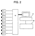
- Fig. 2 shows a principle of the anomalous discharge detection apparatus of the invention.
- the plasma processing equipment includes a processing chamber 1, a wafer 2 placed in the processing chamber 1 for plasma processing thereof, a lower electrode 3 for mounting thereon the wafer 2, an upper electrode 4 facing the lower electrode 3, a blocking condenser 5, an RF power source (high-frequency power source) 6 connected to the lower electrode 3 via the blocking condenser 5, and a ground line 7.
- Injection and exhaustion of a gas are indicated by arrows G1 and G2, respectively.
- the anomalous plasma discharge detection apparatus shown in Figs. 1A and 1B is provided with a multiplicity of ultrasonic detectors 8-15.
- the detection apparatus shown in Fig. 1 is an example which has eight ultrasonic detectors such that the ultrasonic detector 8 is mounted on the lower electrode 3, ultrasonic detector 9 on the upper electrodes 4, and six ultrasonic detectors 10-15 are mounted on the upper and the lower sections of the exterior side walls, angularly spaced apart by 60° along the circumference.
- the anomalous plasma discharge detection apparatus of Fig. 2 has an A/D converter 16, a computer 17, and an anomalous discharge generation/location indicator 18 for indicating the occurrence of an anomalous discharge and the location of the anomalous discharge.
- the ultrasonic detectors 8-15 detect an ultrasonic wave to generate detection signals, which are converted into digital signals by the AD converter 16 and supplied to the computer 17.
- the computer 17 processes and stores the digital signals, determines if an anomalous discharge has occurred, and if it has, determines the source point of the anomalous discharge and issues an alarm for the plasma processing equipment.
- An anomalous discharge location/alarm indicator 18 is provided to indicate the location of the detected anomalous discharge along with an alarm on a monitor.
- Fig. 3 shows an arrangement of any of the ultrasonic detectors 8-15 according to the invention.
- the ultrasonic detector includes: an electrically insulative member (ceramic) 19 coated with a couplant which provides desirable acoustic connection between the ultrasonic detector and the processing chamber; an ultrasonic conversion element 20; an amplifier 21; and a battery 22.
- the couplant-coated insulation member 19 of the ultrasonic detector can be transmitted to the ultrasonic detector without inducing any electric noises.
- Fig. 4 shows a typical waveform L detected by a photosensor and a waveform S detected by an ultrasonic detector of the invention, which were observed by the inventors while studying anomalous discharges in the plasma processing equipment.
- the anomalous fluctuation in plasma radiation detected by the photosensor manifests occurrence of anomalous plasma discharge.
- the output power S0 of the ultrasonic detector varies in the same manner as the radiation by the anomalous plasma discharge during a period L0. This indicates generation of ultrasonic waves accompanying the anomalous plasma discharge. It was confirmed by the inventors that an ultrasonic wave of about 25 kHz is generated during such anomalous discharge.
- an ultrasonic wave accompanying an anomalous plasma discharge is caused by the bombardment of charged particles (e.g. electrons) generated in the anomalous discharge onto the constituent components (e.g. upper electrodes 4) of the plasma processing equipment, or by destruction of surface layers of the components.
- charged particles e.g. electrons
- constituent components e.g. upper electrodes 4
- destruction of surface layers of the components e.g. upper electrodes 4
- AE acoustic emission
- Vpp of the ultrasonic wave is related to the energy ⁇ of the AE event by the following formula.
- Vpp 2 C 1 • C 2 ⁇
- C 1 is a constant which depends on the detection sensitivity of the ultrasonic detector used
- C 2 is a constant which depends on the distance from the source point of the anomalous discharge to the ultrasonic detector, and the energy loss during the propagation over that distance.
- T D / V
- V the speed of the ultrasonic wave, which depends on the materials forming the processing chamber 1
- D the distance from the source point of the anomalous discharge to the detector.
- the location of the anomalous discharge i.e. the source point, can be determined from the different propagation times to the respective detectors.
- the invention converts the analog signals detected by the ultrasonic detectors 8-15 to digital signals by an A/D converter 16, and processes the digital data by a computer 17, as shown in Fig. 2. Since the frequency and the amplitude of an ultrasonic wave generated in an AE event depend on the energy of the AE event and the materials involved in the AE event, the invention compares the waveforms of the ultrasonic waves detected by the ultrasonic detectors 8-15 on the same time axis when the amplitude of these waveforms exceed a predetermined magnitude. From the comparison, relative propagation times of the ultrasonic wave to the respective detectors 8-15, or delay times, with respect to the first detection time by one of the detectors, can be calculated. The maximum range of variation (as shown in Fig. 8) of these waves can be also determined.
- the inventive method of locating the source point of an anomalous plasma discharge in the plasma processing equipment can be described as follows.
- the method includes a procedure for determining whether the source point is on the upper electrode or the lower electrode, or determining the position of the source point on the side wall.
- waveforms output from the ultrasonic detectors 10-15 are compared with each other to find a reference ultrasonic detector, which is one detecting the ultrasonic wave first. From the comparison, delay times T10-T15 for the respective detectors 10-15 with respect to the reference ultrasonic detector are also calculated.
- the waveforms output from the respective ultrasonic detectors appear like ones as shown in Fig. 5.
- the ultrasonic detectors 10, 12, 14 are positioned at the same distance from a support 3A of the lower electrode, detection of the ultrasonic wave by the ultrasonic detector 10 lags behind those of the ultrasonic detectors 12 and 14 by an amount of time to travel across the support 3A, so that the reference detector is either the ultrasonic detector 12 or the ultrasonic detector 14, for which the delay time is zero.
- the source point of the anomalous discharge must be inside the side wall. Otherwise, the discharge source point is outside the side wall. If the source point is determined from these six equations to be anywhere other than the side wall, then the location of the anomalous discharge is considered to be either on the upper or the lower end wall of the plasma processing equipment. This can be determined from the known position of the reference ultrasonic detector and the delay times measured by the ultrasonic detector 8 mounted on the lower electrode 3 and detector 9 on the upper electrode 4.
- the reference ultrasonic detector is either one of the ultrasonic detectors 10, 12, or 14 mounted on the lower end of the side wall, and if the ultrasonic detector 8 has detected the wave earlier than the detector 9, then the source point is determined to be in the lower section of the plasma processing equipment (Fig. 5). Under these conditions, the three simultaneous equations (3.1), (3.3) ,(3.5) for the three ultrasonic detectors 10, 12, and 14 are solved, treating the lower end of the processing chamber 1 coplanar with the side wall as shown in Fig. 9B. When the solution represents a position on the support 3A of the lower electrode 3 lying on the lower end of the processing chamber, it is determined that the source point is on the lower electrode 3, but otherwise, the source point is determined to lie on the lower end of, and inside, the processing chamber.
- the reference ultrasonic detector is either one of the ultrasonic detectors 11, 13, and 15 mounted on the upper end of the side wall, and if the detector 9 detects the wave earlier than the detector 8, it is determined that the discharging source point is in the upper section of the plasma processing chamber.
- the three simultaneous equations (3.2), (3,4) and (3.6) for the ultrasonic detectors 11, 13, and 15 are solved, treating the upper end of the processing chamber 1 as co-planar with the side wall. If the solved position is anywhere other than the support 4A of the upper electrode 4 in the upper section of the processing chamber 1, the discharging source is determined to be on the inner upper end of the processing chamber, but otherwise to be on the upper electrode 4.
- the precision of locating the discharge source point may be improved by providing more ultrasonic detectors at different positions. For example, if additional ultrasonic detectors are mounted on the upper and lower electrodes, the very position of the source points on the electrodes may be determined.
- a characteristic delay time may be computed by the computer 17 by, for example, averaging characteristic delay times associated with characteristic indices of the waves (e.g. height of the waveforms during an anomalous discharge).
- a lookup table may be provided in a memory which defines correspondence between possible locations of the anomalous discharge source point and the patterns of delay times for particular arrangement of the ultrasonic detectors so that, given waveforms of the detected ultrasonic waves, the computer 17 analyzes the delay time pattern to determine the location of the source point with respect to the ultrasonic detectors.
- the constant C 2 of the equation (1) Upon determination of the anomalous discharge source point, the constant C 2 of the equation (1), and hence the energy ⁇ of the AE event, is obtained, since the respective propagation distances and the attenuation losses for these distances are known. From the location and the maximum range of variation of the detected ultrasonic wave thus determined, the level of the acoustic emission (AE) during the anomalous discharge is determined and displayed on a monitor. An alarm may be generated and/or the operation of the processing apparatus may be stopped when the amplitudes of the wave detected by the respective detectors exceed predetermined levels set for respective locations of the plasma processing equipment.
- AE acoustic emission
- the peripheries of upper and lower end walls of the processing chamber are divided into three equal parts and a total of six ultrasonic detectors are arranged one for each part such that any two detectors do not face-to-face, to thereby detect and locate the source point of an anomalous discharge in the processing chamber.
- the inventors have found a further method different from the method of Fig. 1, in which only four detectors are required to determine the location of an anomalous discharge source point.
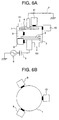
- Fig. 6A shows an example in which ultrasonic detectors are arranged in a plasma processing equipment based on this method.
- Fig. 6B shows in cross sectional view an arrangement of ultrasonic detectors mounted on the processing chamber 1 at the intermediate level thereof.
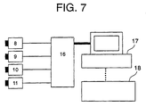
- Fig. 7 shows an exemplary anomalous discharge detection apparatus which utilizes four ultrasonic detectors. It is noted that like reference numerals refer to the same elements in Figs. 1 through 5, so that the description of each element will not be repeated here unless otherwise needed.
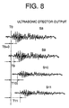
- Fig. 8 compares the outputs S8-S11 of the ultrasonic detectors 8-11 as shown in Fig. 6 when their amplitudes exceed a threshold level.
- T0 is the time at which an ultrasonic wave is first detected by one of the ultrasonic detectors (the detector hereinafter referred to as reference detector);
- Periods T8-T11 are delay times for the respective detectors 8-11 with reference to the detection time of the reference detector.
- Fig. 8 applies to a case where the anomalous discharge source point generating the ultrasonic wave is located on the lower electrode 3 (shown at P1 in Fig. 1).
- the ultrasonic detector 8 is mounted on the lower section of the exterior wall of the processing chamber 1, and the ultrasonic detectors 9 and 10 on the upper section of the exterior wall.
- the reference detector is detector 8, for which the delay time is zero.
- the source point of an anomalous discharge can be located using four ultrasonic detectors in accordance with the invention as follows. It is convenient to define a 2-dimensional XY Cartesian coordinate system to locate the position of the anomalous discharge source point.
- the processing chamber 1 is represented in Fig. 9A by a cylinder having a radius R and a height 2H.
- the XY coordinate system is defined with y axis coinciding the central axis of the cylinder and X axis coinciding a radius of the cylinder passing through the center O of the cylinder, with the origin being at the center O, as shown in Fig. 9A.
- 9B is an expansion plan of the processing chamber 1 onto which XY coordinate system is projected with the origin O projected onto the center of the parallelepiped side wall of the cylinder, and the upper and the lower ends 20 and 22, respectively, of the cylinder projected onto the projected y axis, as shown.
- the positions of the ultrasonic detectors 8-11 of Fig. 6 are marked on the XY plane by dots A1 through A4.
- Fig. 6 illustrates an arrangement of ultrasonic detectors for which areas of the processing chamber are divided into four substantially equal sections as even as possible in order to attain uniform precision of measurements by the detectors.
- the distances D8-D11 can be expressed in terms of the coordinates (x, y) of the source point, so that the equations (4.1) - (4.3) are actually a set of equations involving only two variables x and y.
- the coordinates (x, y) can be determined by Eq. (4.1) and (4.2).
- Figs. 10A-10D show typical cases where an ultrasonic wave propagates from an anomalous discharge source point P to an ultrasonic detector A.
- Fig. 10A shows a coplanar path on the side wall
- Fig. 10B a non-coplanar propagation path from a point on the upper end wall of the processing chamber to a point on the side wall
- Fig. 10C a non-coplanar propagation path from a point on the side wall to another point on the side wall through the upper end wall
- Fig. 10D a propagation path from a point on the upper end wall to a point on the lower end wall through the side wall.
- the shortest path crosses the circumference of the upper end wall at a point where the radius of the upper end wall makes an angle with y axis, and the shortest distance D depends on ⁇ as well as on the position (x, y) of the discharge source point P.
- the equations (4.1) - (4.3) involves ⁇ in addition to x and y.
- the equations are difficult to solve. Further, the equations must be modified, loosing their generality, every time the position of the ultrasonic detector is changed.
- Newton's method is used to quickly obtain an accurate approximate solution.
- x 0 and y 0 of x and y are recursively calculated until their absolute values become arbitrarily small.
- ⁇ is set to an arbitrary value ⁇ 0 , so that the value of g ( ⁇ ) is g 0 .
- ⁇ is obtained by inserting the values of g ( ⁇ ) and ⁇ g/ ⁇ ⁇ thus obtained in Eq. (8).
- the asymptotic method involves only one angle specifying the shortest propagation path from an anomalous source point to a given ultrasonic detector.
- the method may be applied to cases which involve two angular variables ⁇ 1 , ⁇ 2 , as shown in Figs. 10C and 10D.
- the shortest distance D may be obtained using the following equations.
- This procedure is repeated by shifting x and y from the initial values x 0 and y 0 , respectively, by- ⁇ x and - ⁇ y, respectively, until ⁇ x and ⁇ y become less than a permissible error limit. It should be noted that different source points can result if the initial values x 0 and y 0 are not appropriate. To find appropriate initial values x 0 and y 0 , some preliminary calculations must be made using Eqs. (6.1) and (6.2).
- any anomalous discharge that takes place at any point of the plasma processing equipment can be determined correctly by choosing the initial position (x 0 , y 0 ) at either centers of the upper and the lower end walls.
- the procedure will be ended if only one source point of the anomalous discharge is found. However, if more than one source coordinates are found, a further determination of the correct source point must be determined by calculating the left hand side of Eq. (4.3) for the multiple source points obtained. The coordinates having the smallest value of the left hand side of Eq. (4.3) is determined as the correct source point. In this way, using the method of the invention, it is possible to locate a desirable asymptotic position of the source point by means of only four ultrasonic detectors.
- Fig. 12 is a flowchart illustrating briefly an inventive method of locating the source point of an anomalous discharge from waveforms detected by four ultrasonic detectors.
- the four ultrasonic detectors mounted on appropriate sections of the processing chamber will detect ultrasonic wave as shown in Fig. 8 (block B1).
- the ultrasonic detector that has first detected the ultrasonic wave at time T0 is chosen as the reference detector, and the delay times T9 - T11 of the rest of the detectors relative to T0 are calculated (block B2).
- the region of the plasma processing chamber accessible to anomalous discharges may be divided into sub-regions such that each region always has a true asymptotic source point among other possible (i.e. competing) source points, irrespective of the position of the first source point so long as a first asymptotic point is chosen within that region.
- a true source point of the anomalous discharge is determined among the possible source points. This can be done by choosing the asymptotic point which satisfies Eq. (4.3) best as the correct source point, since the true asymptotic solution satisfies Eq. (4.3).
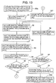
- Figs. 13 and 14 together represent a flowchart of determining correct asymptotic solution (i.e. correct source point) based on the Newton's method, by repeating the asymptotic approximation for each of the predetermined sub-regions in turn by setting up a first asymptotic point in each sub-region, for example, first in the upper end wall (block 63A), and next on the lower end wall of the processing chamber (block 64B), and so on, so long as no correct asymptotic solution is found in the current sub-region.
- correct asymptotic solution i.e. correct source point
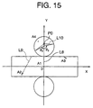
- step S1 if an anomalous discharge as shown in Fig. 8 is detected, the initial asymptotic point is chosen at position P0 on the upper end wall as shown in Fig. 15, assuming that the anomalous discharge source point lies on the upper end wall (block B3A).
- the distances from P0 to the positions A1, A2, and A3 of the ultrasonic detectors 8 - 10, respectively, are L8, L9, and L10 as shown in Fig. 15.
- the distances L9 and L10 involves angles ⁇ 2 and ⁇ 3 , respectively. Therefore, the shortest distances D9 and D10 must be obtained from the distances L9 and L10, respectively.
- step S2 the shortest distances D9 and D10 are determined using the method that follows, using the distance L9 and g 1 given by the following respective equations.
- L9 (X 0 -rsin ⁇ 2 ) 2 +(y 0 -h-r+rcos ⁇ 2 ) 2 + (r ⁇ 2 -x 2 ) 2 +(h-y 2 ) 2
- g 1 ⁇ L9/ ⁇ ⁇ 2
- the value g 11 of g 1 is determined for the angle ⁇ 2 evaluated at ⁇ 20 + ⁇ 20 , which gives the following results.
- the value ⁇ 2 of ⁇ is obtained. If the value of ⁇ 2 is not within a predetermined range of accuracy, the angle is incremented further by ⁇ 2 , to renew the value thereof, using Eq. (8). This procedure will be repeated until the magnitude of ⁇ 2 falls within the predetermined range of accuracy, when the resultant asymptotic angle ⁇ 20 - ⁇ 2 is identified as the angle ⁇ for the path having the shortest distance. It is noted that since the distance function L( ⁇ ) may have multiple minima, different initial positions should be tried to obtain ⁇ by the asymptotic method. Of the distances associated with these first asymptotic points, the minimum one is the true shortest distance.
- the angle ⁇ 3 for the shortest path L10 is obtained by the Newton's method. Substitution of ⁇ 3 in L9 and L10 provides the shortest distances D9 and D10 (step S2). Incidentally, the shortest distance D8 is given as the length of a straight line segment L8 between P0 and A1.
- the shortest distances D8x, D9x, and D10x are calculated for a first asymptotic position which is a small distance ⁇ x 0 away from the initial position in the direction of X in the same manner as in step S2.
- the shortest distances D8y, D9y, and D10y are calculated for a further position a small distance ⁇ y 0 away from the initial position in just the same way as in step S2.
- step S5 the amount of shifts ⁇ x and ⁇ y for the next asymptotic position are determined from the shortest distances and the values of ⁇ 1 and ⁇ 2 obtained in steps S2-S4, as follows.
- step S6 a second position (x 0 - ⁇ x, y 0 - ⁇ y) better (i.e. closer to the asymptotic solution) than the first asymptotic position can be obtained.
- this point is checked whether or not it is on the upper end wall of the processing chamber. If it is, then the procedure proceeds to step S7, where the magnitudes of ⁇ x and ⁇ y are checked to see if the position is sufficiently close to the pertinent source point of anomalous discharge. If it is determined in step S7 that the magnitudes of ⁇ x and ⁇ y are not within the predetermined range of accuracy, the second asymptotic position is further shifted by - ⁇ x and - ⁇ y in step S8.
- step S6 the procedure proceeds to step S10 (Fig. 14), where a position P2 is chosen on the side wall as the initial position for the recursive estimation to find the asymptotic solution on the side wall.
- the choice of P1 is made by mapping P1 to P2 such that P2 lies on the perpendicular dropped from one point of the upper end of the side wall and located at a distance r ⁇ from the center line of the side wall, where r is the radius of the upper end wall and ⁇ is the angle of the radial vector for P1, as shown in Fig. 16.
- the distance between the upper end of the side wall and the position P2 equals the length of the radial vector P1 minus radius r.
- a similar recursive estimation of the source point starting from the position P2 provides an asymptotic position closer to the source point. It should be noted that there can be more than one propagation paths, for example a direct path "a” which runs only within the side wall and a path "c" which runs across the upper end wall of the processing chamber as shown in Fig. 17. Therefore, it is necessary to determine which of the paths is actually the shortest one by calculating the lengths of the paths.
- step S15 If it is determined in step S15 that the values of ⁇ x and ⁇ y obtained in step S14 provide an asymptotic position outside the side wall, then an alternative position is found by an opposite mapping as compared with the mapping used in step S10, and a determination is made in step S17 as to which sub-region the mapped position belongs to. If the mapped position is on the lower end wall, then this position is employed in step S20 as the first point of the recursive calculation for the asymptotic source point on the lower end wall. The procedure then proceeds to block 3B to obtain a final asymptotic source point on the lower end wall.
- step S21 the position is used as the first position for the recursive calculation for the asymptotic source point on the assumption that the anomalous discharge source point lies on the upper end wall.
- step S2 of block B3a the procedure proceeds to step S2 of block B3a to continue asymptotic determination of the source point.
- block B3b a similar calculation is made to find the asymptotic source point on the lower end wall assuming the anomalous discharge source point to lie on the lower end wall, as in block B3a, starting from the mapped position. After all the possible asymptotic positions of the source point are determined for the different first positions, the true asymptotic source point is determined in block B4.
- a loop is provided in the example shown in Figs. 13 and 14 for sequentially finding alternative asymptotic source points in each of the different sub-regions when the first asymptotic source point calculated in steps S10, S20, or S21 is outside a presumed sub-region. Because of this loop, a better asymptotic source point which is closer to the true source point can be quickly found by changing the first asymptotic source point. It would be understood that a multiplicity of first asymptotic positions may be simultaneously set up (in step S1 for example) in blocks B3a and B3b to sequentially obtain possible asymptotic source points.
- Fig. 18 shows propagation paths e, f, and g of an ultrasonic wave emitted from an anomalous discharge source point at position P on the lower electrode 23 to the respective ultrasonic detectors 8, 9, and 10.
- numerals 22 and 24 indicate a lower end wall and a lower electrode support, respectively.
- Eqs. (4.1) - (4.3) enables calculation of differences in the propagation distance from the source point to the respective detectors.
- the distances from the source point at P to the respective detectors 8, 9, and 10 are the distances to the points E, F, and G.
- the asymptotic source point on the electrode or electrode support may be determined to lie on the upper/lower end wall of the processing chamber and within a certain distance from the corresponding electrode support. For example, in the 2-dimensional coordinate system, if the anomalous discharge source point is determined to be on the electrode/electrode support, the asymptotic source point is found on the electrodes or on the electrode support, but the precise position of the source point cannot be determined.
- FIG. 19A shows a cross section of an AE sensor 30, which is typically an ultrasonic detector available on the market.
- the AE sensor 30 is adapted to detect an ultrasonic stress and convert the pressure into an electric signal.
- the sensor 30 includes a main body 31, an output connector 32 for outputting the electric signal, and an insulating film 33.
- Fig. 19B shows a cross section of an AE sensor hold case 34 for housing therein the AE sensor 30 and for securely holding it in position.
- the AE sensor hold case 34 has a lower cover 35 and an upper cover 36.
- the lower case 35 has a generally planar configuration and has a convex surface one side thereof adapted to be glued onto the exterior of the processing chamber and a polished flat surface on the other side thereof to receive thereon the AE sensor.
- the upper cover 36 has a generally cylindrical configuration so as to cover entirely the AE sensor 30 mounted on the lower cover 35.
- the AE sensor hold case 33 includes a couplant 39 (made of grease for example), a holding member 40 (bushing for example) for holding the AE sensor 30 at a predetermined position on the lower cover 35, a resilient shock absorbing member 41 such as an O-ring and a spring, and an insulation coat 42 such as alumite.
- the upper cover 36 has an opening 36H for leading the output connector of the AE sensor out of the sensor hold case, and a conductive contact 43 for keeping the upper cover 36 and the AE sensor 30 at the same electric potential.
- Figs. 20 and 21 illustrate how the AE sensor of the invention is installed in the AE sensor hold case 34.
- Fig. 20 shows a process of mounting the AE sensor in the case
- Fig. 21 a final condition of the AE sensor thus mounted.
- threaded bores 35H for receiving the screws 37
- a fixing glue (epoxy glue) 44 for fixing the AE sensor hold case on the exterior 50 of the processing chamber.
- the lower cover 35 of the AE sensor hold case 33 is securely fixed at an appropriate exterior section 50 of the processing chamber 13 with glue 44.
- the lower surface of the lower cover 35 is adequate configured to fit on the exterior wall of the processing chamber 13, so that it can be easily glued on the wall.
- the AE sensor hold case 33 is insulated by the insulation coat 42.
- the insulative film 33 of the AE sensor 30 is inserted in the holding member 40, the output connector 32 into the opening 36H of the upper cover 36, and coupling screws 37 into the threaded bores 35h formed in the lower cover 35 to firmly secure the upper cover 36 to the lower cover 35.
- the holding member 40 can be a rubber bushing in the form of O-ring for example, adapted to hold the AE sensor 30 in position on the lower cover 35 and prevent the AE sensor 30 from contacting the upper cover 36 while mounting the AE sensor 30 on the lower cover 35.
- the resilient member 41 serves to prevent direct contact of the AE sensor 30 with the upper cover 36 thereby preventing the ultrasonic stress that has entered the upper case 36 via the coupling screws 37 from further propagating to the AE sensor.
- the resilient member 41 also serves to adequately keep the AE sensor of the upper cover 35 in forced contact with the couplant 39, thereby causing the ultrasonic wave entering the case to be efficiently transmitted to the AE sensor 30.
- the insulation coat 42 is provided to maintain electric insulation between the AE sensor hold case 33 and the plasma processing equipment when the former case is mounted on the exterior of the latter apparatus.
- the electric contacts 43 can be a metallic spring adapted to securely hold the upper and the lower covers in electric contact when they are coupled together, thereby bringing them to the same electric potential and hence reducing electric noise which is otherwise detected by the AE sensor 30.
- the acoustic insulation member 37 is provided to prevent the propagation of the ultrasonic wave traveling in the wall of the processing chamber into the upper cover 36 and possible resonance of the AE sensor hold case 33 caused by the ultrasonic wave.
- Fig. 22 is a cross sectional view of the AE hold sensor case 33 which has in the side wall thereof the opening 36H for leading the output connector 32 of the AE sensor 30 out of the case 33, instead of leading the output connector 32 through the upper end of the case as shown in Fig. 19A.
- anomalous plasma discharges can be quickly and accurately detected using a method and an apparatus according to the invention.
- the position of an anomalous plasma discharge in a plasma processing equipment can be located by measuring and comparing on the same time axis the delay times in the propagation of the ultrasonic wave accompanying the anomalous plasma discharge, using a multiplicity of ultrasonic detectors (e.g. AE sensors) arranged on a vacuum chamber and/or discharge electrodes of the plasma processing equipment.
- a multiplicity of ultrasonic detectors e.g. AE sensors
- occurrence of an anomalous discharge during a plasma processing and the magnitude (intensity) of the acoustic shock (AE) caused by the anomalous discharge can be automatically and accurately detected, which permits automated control of the plasma processing equipment and hence prevents production of defective products.
- the invention allows positive prevention of occurrence of such anomalous plasma discharges, thereby permitting efficient management of the plasma processing equipment, especially of consumable parts of the apparatus. It would be appreciated that the invention can be applied to the detection of anomalous discharge in RF plasmas and detection of anomalous sparks and arcs in DC plasmas of DC sputters as well.
- anomalous plasma discharges can be detected and evaluated by a delay time-distance relationship, from the measurements of the delay times by four ultrasonic detectors mounted in or on a plasma processing equipment. It should be appreciated that the invention has a great flexibility to reduce the installation cost of the anomalous discharge detection apparatus in that the four sensors can be of any type and placed at arbitrary positions.
- An AE sensor hold case of the invention is a dedicated case which is designed to be acoustically coupled with the AE sensors mounted on the lower cover, which is glued to the wall of a processing chamber so that ultrasonic waves propagating from an anomalous discharge to the lower cover can be efficiently detected by the AE sensors.
- the use of such dedicated case provides a simple and safe way of mounting/dismounting the AE sensors for maintenance without suffering from destruction and deterioration during mounting/dismounting, and hence maintain precision of the AE sensors.
Landscapes
- Physics & Mathematics (AREA)
- Chemical & Material Sciences (AREA)
- Analytical Chemistry (AREA)
- Health & Medical Sciences (AREA)
- General Health & Medical Sciences (AREA)
- General Physics & Mathematics (AREA)
- Immunology (AREA)
- Life Sciences & Earth Sciences (AREA)
- Biochemistry (AREA)
- Engineering & Computer Science (AREA)
- Pathology (AREA)
- Plasma & Fusion (AREA)
- Acoustics & Sound (AREA)
- Toxicology (AREA)
- Signal Processing (AREA)
- Organic Chemistry (AREA)
- Chemical Kinetics & Catalysis (AREA)
- Spectroscopy & Molecular Physics (AREA)
- Plasma Technology (AREA)
- Investigating Or Analyzing Materials By The Use Of Ultrasonic Waves (AREA)
- Drying Of Semiconductors (AREA)
- Physical Vapour Deposition (AREA)
- Chemical Vapour Deposition (AREA)
Abstract
Description
After all the possible asymptotic positions of the source point are determined for the different first positions, the true asymptotic source point is determined in block B4.
Claims (19)
- An anomalous plasma discharge detection apparatus for use with a plasma processing equipment, comprising:a multiplicity of ultrasonic detection means for detecting ultrasonic waves accompanying an anomalous plasma discharge in said plasma processing equipment, and for generating signals indicative of the ultrasonic wave detected (ultrasonic signals);data processing means for processing waveforms of said ultrasonic wave signals ; andmonitor means for displaying a signal indicative of said anomalous discharge.
- The anomalous plasma discharge detection apparatus according to claim 1, further comprising electrically insulated mounting means for mounting said ultrasonic detection means on said plasma processing means in an electrically insulated condition.
- The anomalous plasma discharge detection apparatus according to claim 1, whereinsaid multiplicity of ultrasonic detection means are mounted on predetermined sections of said plasma processing equipment, andsaid data processing means is adapted to determine the location of an anomalous plasma discharge based on the propagation time differences of said ultrasonic wave from said source point to the respective multiple ultrasonic detection means.
- The anomalous plasma discharge detection apparatus according to claim 3, wherein said ultrasonic detection means are provided with electrically insulated mounting means for mounting said ultrasonic detection means on said plasma processing equipment in an electrically insulated condition.
- The anomalous plasma discharge detection apparatus according to claim 3, comprising four ultrasonic detection means, installed on the walls of said plasma processing chamber, for use in the determination of the location of said source point by an asymptotic approximation method.
- The anomalous plasma discharge detection apparatus according to claim 1, further comprising:means for determining the level of an anomalous event (AE) generating an ultrasonic wave by processing waveforms of said ultrasonic wave processed by said data processing means; andmeans for generating an alarm for issuing an alarm when said level exceeds a given threshold.
- The anomalous plasma discharge detection apparatus according to claim 6, wherein said ultrasonic detection means are provided with electrically insulated mounting means for mounting said ultrasonic detection means on said plasma processing equipment in an electrically insulated condition.
- The anomalous plasma discharge detection apparatus according to claim 1, further comprising:means for determining the level of an anomalous event (AE) generating an ultrasonic wave by processing waveforms of said ultrasonic wave processed by said data processing means; andmeans for generating an alarm for issuing an alarm when said level exceeds a given threshold.
- The anomalous plasma discharge detection apparatus according to claim 8, wherein said ultrasonic detection means are provided with electrically insulated mounting means for mounting said ultrasonic detection means on said plasma processing equipment in an electrically insulated condition.
- A method of detecting an anomalous plasma discharge in a plasma processing equipment, comprising steps of placing a multiplicity of ultrasonic detection means at predetermined positions of said plasma processing equipment.
- A method of detecting an anomalous plasma discharge in a plasma processing equipment, comprising steps of:mounting four ultrasonic detection means at predetermined positions of said plasma processing equipment; andlocating the source point of said anomalous plasma discharge based on the propagation time differences of an ultrasonic wave propagating from said source point to the respective multiple ultrasonic detection means.
- The method of detecting an anomalous plasma discharge according to claim 11, wherein said method uses four ultrasonic detection means, and said step of locating the anomalous plasma discharge is an asymptotic approximation of the position of said source point through recursive calculations of the distances between said source point to the respective ultrasonic detection means from said propagation time differences, using known relationships between said distances and said propagation time differences.
- An acoustic sensor hold case for accommodating an AE sensor, said hold case having one side to be glued onto an exterior of a processing chamber of a plasma processing equipment, said hold case comprising:a generally slab shaped lower cover having a polished flat inner surface for acoustically coupling said one side with said AE sensor;a generally cylindrical upper cover for enclosing said AE sensor, whereinsaid upper and lower covers are configured to be connected together by screws to firmly secure said AE sensor in position in said hold case so that the input end of said AE sensor is abutted against said inner surface of said lower cover with an adequate pressure, providing acoustic coupling therebetween.
- The acoustic sensor hold case according to claim 13, further comprising at an inner upper position of said upper cover a resilient member which causes said input end of said AE sensor abuts against a couplant coated on the inner surface of said lower cover with an adequate pressure when said upper and the lower covers are coupled together.
- The acoustic sensor hold case according to claim 13, wherein only said one end of said AE sensor hold case is covered with an electrically insulative film.
- The acoustic sensor hold case according to claim 13, further comprising at an inner upper section of said upper case an electrically conductive contact which abuts against said AE sensor, thereby bringing said AE sensor and said upper case to the same electric potential when said upper and lower covers are coupled together.
- The acoustic sensor hold case according to claim 13, further comprising an acoustically insulative member between the contacting surfaces of said upper and lower covers.
- The acoustic sensor hold case according to claim 13, wherein said upper cover is provided in either the upper end or the side wall thereof with an opening for passing therethrough an output connector of said AE sensor.
- The acoustic sensor hold case according to claim 13, further comprising a rubber bushing lying along the inner periphery of said lower cover and extending along the external periphery of said AE sensor such that said bushing keeps said AE sensor not in direct contact with said upper cover when said upper and lower covers are coupled together.
Applications Claiming Priority (3)
| Application Number | Priority Date | Filing Date | Title |
|---|---|---|---|
| JP2000089840 | 2000-03-28 | ||
| JP2000089840 | 2000-03-28 | ||
| PCT/JP2001/002536 WO2001074123A1 (en) | 2000-03-28 | 2001-03-28 | Apparatus for detecting plasma anomalous discharge and method of detecting the same |
Publications (2)
| Publication Number | Publication Date |
|---|---|
| EP1189491A1 true EP1189491A1 (en) | 2002-03-20 |
| EP1189491A4 EP1189491A4 (en) | 2007-09-26 |
Family
ID=18605539
Family Applications (1)
| Application Number | Title | Priority Date | Filing Date |
|---|---|---|---|
| EP01917520A Withdrawn EP1189491A4 (en) | 2000-03-28 | 2001-03-28 | PLASMA ABNORMAL DISCHARGE DETECTION APPARATUS, AND CORRESPONDING DETECTION METHOD |
Country Status (8)
| Country | Link |
|---|---|
| US (1) | US6753499B1 (en) |
| EP (1) | EP1189491A4 (en) |
| JP (1) | JP3569898B2 (en) |
| KR (1) | KR100530688B1 (en) |
| CN (1) | CN1222762C (en) |
| DE (1) | DE1189491T1 (en) |
| TW (1) | TW505939B (en) |
| WO (1) | WO2001074123A1 (en) |
Cited By (3)
| Publication number | Priority date | Publication date | Assignee | Title |
|---|---|---|---|---|
| US7334477B1 (en) * | 2004-12-22 | 2008-02-26 | Lam Research Corporation | Apparatus and methods for the detection of an arc in a plasma processing system |
| WO2009135919A1 (en) * | 2008-05-07 | 2009-11-12 | Dublin City University | A system for analysing plasma |
| EP3410131A1 (en) * | 2017-05-09 | 2018-12-05 | Siemens Aktiengesellschaft | Method and apparatus for the localisation of an electric discharge in an electrical installation |
Families Citing this family (39)
| Publication number | Priority date | Publication date | Assignee | Title |
|---|---|---|---|---|
| JP3717467B2 (en) * | 2002-05-02 | 2005-11-16 | 株式会社日立製作所 | Semiconductor processing apparatus and diagnostic method for semiconductor processing apparatus |
| TW558789B (en) * | 2002-05-02 | 2003-10-21 | Hitachi High Tech Corp | Semiconductor processing device and diagnostic method of semiconductor processing device |
| DE102004015090A1 (en) | 2004-03-25 | 2005-11-03 | Hüttinger Elektronik Gmbh + Co. Kg | Arc discharge detection device |
| JP4594646B2 (en) * | 2004-05-17 | 2010-12-08 | 住友金属工業株式会社 | Damage detection method for partial discharge and damage detection apparatus for partial discharge |
| JP4673601B2 (en) * | 2004-10-27 | 2011-04-20 | 東京エレクトロン株式会社 | Plasma processing equipment |
| US20060100824A1 (en) * | 2004-10-27 | 2006-05-11 | Tokyo Electron Limited | Plasma processing apparatus, abnormal discharge detecting method for the same, program for implementing the method, and storage medium storing the program |
| US7305311B2 (en) * | 2005-04-22 | 2007-12-04 | Advanced Energy Industries, Inc. | Arc detection and handling in radio frequency power applications |
| JP4674363B2 (en) * | 2005-06-27 | 2011-04-20 | 独立行政法人産業技術総合研究所 | Abnormal state detection method and sheet-like piezoelectric sensor |
| JP5094002B2 (en) | 2005-09-06 | 2012-12-12 | ルネサスエレクトロニクス株式会社 | Plasma processing apparatus and method for suppressing abnormal discharge thereof |
| DE502005006550D1 (en) * | 2005-12-22 | 2009-03-12 | Huettinger Elektronik Gmbh | Method and device for arc detection in a plasma process |
| JP4754419B2 (en) * | 2006-07-03 | 2011-08-24 | 学校法人立命館 | Plasma abnormal discharge diagnostic method, plasma abnormal discharge diagnostic system, and computer program |
| ATE448562T1 (en) * | 2006-11-23 | 2009-11-15 | Huettinger Elektronik Gmbh | METHOD FOR DETECTING AN ARC DISCHARGE IN A PLASMA PROCESS AND ARC DISCHARGE DETECTION DEVICE |
| US7795817B2 (en) * | 2006-11-24 | 2010-09-14 | Huettinger Elektronik Gmbh + Co. Kg | Controlled plasma power supply |
| EP1928009B1 (en) * | 2006-11-28 | 2013-04-10 | HÜTTINGER Elektronik GmbH + Co. KG | Arc detection system, plasma power supply and arc detection method |
| EP1933362B1 (en) * | 2006-12-14 | 2011-04-13 | HÜTTINGER Elektronik GmbH + Co. KG | Arc detection system, plasma power supply and arc detection method |
| US8217299B2 (en) * | 2007-02-22 | 2012-07-10 | Advanced Energy Industries, Inc. | Arc recovery without over-voltage for plasma chamber power supplies using a shunt switch |
| ATE493749T1 (en) | 2007-03-08 | 2011-01-15 | Huettinger Elektronik Gmbh | METHOD AND DEVICE FOR SUPPRESSING ARC DISCHARGES DURING OPERATING A PLASMA PROCESS |
| JP4874200B2 (en) * | 2007-09-20 | 2012-02-15 | 新日本製鐵株式会社 | Detection method of crack occurrence position during press forming |
| US9074285B2 (en) * | 2007-12-13 | 2015-07-07 | Lam Research Corporation | Systems for detecting unconfined-plasma events |
| US8158017B2 (en) * | 2008-05-12 | 2012-04-17 | Lam Research Corporation | Detection of arcing events in wafer plasma processing through monitoring of trace gas concentrations |
| US8395078B2 (en) | 2008-12-05 | 2013-03-12 | Advanced Energy Industries, Inc | Arc recovery with over-voltage protection for plasma-chamber power supplies |
| EP2648209B1 (en) | 2009-02-17 | 2018-01-03 | Solvix GmbH | A power supply device for plasma processing |
| JP5363213B2 (en) * | 2009-06-30 | 2013-12-11 | 東京エレクトロン株式会社 | Abnormality detection system, abnormality detection method, storage medium, and substrate processing apparatus |
| US8552665B2 (en) | 2010-08-20 | 2013-10-08 | Advanced Energy Industries, Inc. | Proactive arc management of a plasma load |
| CN102566475B (en) * | 2010-12-17 | 2015-07-08 | 北京北方微电子基地设备工艺研究中心有限责任公司 | Method and device for processing monitoring alarm and plasma processing device |
| JP5741315B2 (en) * | 2011-08-16 | 2015-07-01 | 東京エレクトロン株式会社 | Film crack detection apparatus and film formation apparatus |
| JP2014022594A (en) * | 2012-07-19 | 2014-02-03 | Tokyo Electron Ltd | Film crack detector and deposition apparatus |
| TW201432279A (en) * | 2013-02-05 | 2014-08-16 | Tzu-Feng Wanglee | Method of utilizing vocal features for determining malfunctions of electrical equipment caused by arc discharge, mechanical vibration and abnormal displacement |
| CN107817425B (en) * | 2017-10-11 | 2024-01-16 | 国网辽宁省电力有限公司电力科学研究院 | Identification method and detection system for authentic and fake discharge sources in transmission lines |
| US11565365B2 (en) * | 2017-11-13 | 2023-01-31 | Taiwan Semiconductor Manufacturing Co., Ltd. | System and method for monitoring chemical mechanical polishing |
| JP7183090B2 (en) * | 2019-03-20 | 2022-12-05 | 東京エレクトロン株式会社 | Plasma processing method and plasma processing apparatus |
| US11688413B2 (en) | 2019-12-19 | 2023-06-27 | Taiwan Semiconductor Manufacturing Co., Ltd. | Method and system for audio recognition of arcing during semiconductor process |
| US20210217588A1 (en) * | 2020-01-10 | 2021-07-15 | COMET Technologies USA, Inc. | Azimuthal sensor array for radio frequency plasma-based wafer processing systems |
| CN111257727A (en) * | 2020-01-17 | 2020-06-09 | 上海华力集成电路制造有限公司 | Device and method for detecting arc discharge in WAT test |
| CN112635285B (en) * | 2020-12-03 | 2023-12-12 | 长江存储科技有限责任公司 | Monitoring method and system for arc discharge in plasma process chamber |
| JP7592564B2 (en) * | 2021-07-21 | 2024-12-02 | 株式会社ニューフレアテクノロジー | Discharge part detection method and discharge part detection device |
| US11808800B2 (en) * | 2021-11-18 | 2023-11-07 | National Technology & Engineering Solutions Of Sandia, Llc | Radioimaging for real-time tracking of high-voltage breakdown |
| CN114383805B (en) * | 2022-03-23 | 2022-05-31 | 中国空气动力研究与发展中心超高速空气动力研究所 | Measurement system and measurement method of discharge drag reduction equipment |
| JP2026023209A (en) * | 2024-07-31 | 2026-02-13 | 株式会社Kokusai Electric | Substrate processing apparatus, detection method, semiconductor device manufacturing method, and program |
Family Cites Families (20)
| Publication number | Priority date | Publication date | Assignee | Title |
|---|---|---|---|---|
| JPS5823895B2 (en) | 1976-05-25 | 1983-05-18 | 岩崎通信機株式会社 | Vibration source position detection method and device |
| CH655032A5 (en) * | 1982-06-30 | 1986-03-27 | Mitsubishi Electric Corp | ELECTRIC DISCHARGE MACHINE FOR ELECTRO-EROSION. |
| US4582974A (en) * | 1982-08-02 | 1986-04-15 | Mitsubishi Denki Kabushiki Kaisha | Electric discharge machine including means for detecting abnormal discharge conditions |
| JPS59111231A (en) * | 1982-12-16 | 1984-06-27 | Japan Atom Energy Res Inst | System for detecting abnormal arc discharge |
| DE3329134C2 (en) | 1983-08-12 | 1985-06-20 | Deutsche Forschungs- und Versuchsanstalt für Luft- und Raumfahrt e.V., 5000 Köln | Device for measuring cross-sections on objects, in particular on body parts |
| JPS6232364A (en) | 1985-08-06 | 1987-02-12 | Shinotesuto Kenkyusho:Kk | Method for measuring unsaturated iron bonding power in serum |
| JPH0535333Y2 (en) * | 1985-08-13 | 1993-09-08 | ||
| JPS62294921A (en) * | 1986-06-14 | 1987-12-22 | Omron Tateisi Electronics Co | Ultrasonic wave detector |
| JPH07116452B2 (en) * | 1986-06-23 | 1995-12-13 | 株式会社ジャパンエナジー | Method for producing highly aromatic base oil |
| DE3891415T1 (en) | 1988-10-26 | 1991-01-10 | Inst Elektroswarki Patona | METHOD FOR CONTROLLING THE OPERATIONAL SUITABILITY OF A PLASMATRON ELECTRODE AND DEVICE FOR IMPLEMENTING IT |
| JPH03251026A (en) * | 1990-02-28 | 1991-11-08 | Meidensha Corp | Partial discharge detector |
| JPH06265338A (en) | 1993-03-10 | 1994-09-20 | Ngk Insulators Ltd | Accident sound source point standardizing apparatus |
| JPH0755874A (en) | 1993-08-12 | 1995-03-03 | Toyo Electric Mfg Co Ltd | Partial discharge detection method for high voltage rotating electric machine |
| JP3501827B2 (en) | 1993-10-14 | 2004-03-02 | 株式会社デンソー | Cooling cycle |
| JPH08220076A (en) | 1995-02-17 | 1996-08-30 | Toyo Electric Mfg Co Ltd | AE sensor device |
| JPH1074734A (en) | 1996-09-02 | 1998-03-17 | Toshiba Corp | Plasma processing apparatus and semiconductor device manufacturing method |
| US5810963A (en) * | 1995-09-28 | 1998-09-22 | Kabushiki Kaisha Toshiba | Plasma processing apparatus and method |
| GB9522949D0 (en) * | 1995-11-09 | 1996-01-10 | M & A Packaging Serv Ltd | Fill level measuring |
| JPH09145346A (en) | 1995-11-29 | 1997-06-06 | Nagoya Denki Kogyo Kk | Position measurement method of target |
| CN2296285Y (en) | 1996-11-09 | 1998-11-04 | 何立刚 | Dynamic monitor for temperature and air pressure of automobile tyre |
-
2001
- 2001-03-14 TW TW090105981A patent/TW505939B/en not_active IP Right Cessation
- 2001-03-28 US US09/980,379 patent/US6753499B1/en not_active Expired - Fee Related
- 2001-03-28 JP JP2001570688A patent/JP3569898B2/en not_active Expired - Fee Related
- 2001-03-28 CN CNB01800699XA patent/CN1222762C/en not_active Expired - Fee Related
- 2001-03-28 WO PCT/JP2001/002536 patent/WO2001074123A1/en not_active Ceased
- 2001-03-28 EP EP01917520A patent/EP1189491A4/en not_active Withdrawn
- 2001-03-28 KR KR10-2001-7014922A patent/KR100530688B1/en not_active Expired - Fee Related
- 2001-03-28 DE DE1189491T patent/DE1189491T1/en active Pending
Cited By (3)
| Publication number | Priority date | Publication date | Assignee | Title |
|---|---|---|---|---|
| US7334477B1 (en) * | 2004-12-22 | 2008-02-26 | Lam Research Corporation | Apparatus and methods for the detection of an arc in a plasma processing system |
| WO2009135919A1 (en) * | 2008-05-07 | 2009-11-12 | Dublin City University | A system for analysing plasma |
| EP3410131A1 (en) * | 2017-05-09 | 2018-12-05 | Siemens Aktiengesellschaft | Method and apparatus for the localisation of an electric discharge in an electrical installation |
Also Published As
| Publication number | Publication date |
|---|---|
| KR100530688B1 (en) | 2005-11-28 |
| EP1189491A4 (en) | 2007-09-26 |
| WO2001074123A1 (en) | 2001-10-04 |
| US6753499B1 (en) | 2004-06-22 |
| TW505939B (en) | 2002-10-11 |
| CN1365596A (en) | 2002-08-21 |
| CN1222762C (en) | 2005-10-12 |
| JP3569898B2 (en) | 2004-09-29 |
| DE1189491T1 (en) | 2003-06-26 |
| KR20020029328A (en) | 2002-04-18 |
Similar Documents
| Publication | Publication Date | Title |
|---|---|---|
| US6753499B1 (en) | Method and apparatus for detecting anomalous discharge in plasma processing equipment using weakly-ionized thermal non-equilibrium plasma | |
| JP4607517B2 (en) | Plasma processing equipment | |
| KR100676833B1 (en) | Plasma treatment device to evaluate process performance | |
| JPWO2001074123A1 (en) | Anomalous plasma discharge detection device and detection method | |
| KR100582013B1 (en) | Window type probe, plasma monitoring device, and plasma processing device | |
| US7345428B2 (en) | Transducer package for process control | |
| US7334477B1 (en) | Apparatus and methods for the detection of an arc in a plasma processing system | |
| CN101595238A (en) | Method and apparatus for detecting a fault condition in a plasma processing reactor | |
| US20100148769A1 (en) | Non-contact plasma-monitoring apparatus and method and plasma processing apparatus | |
| KR20100004065A (en) | Plasma processing apparatus and plasma processing method | |
| KR20020055343A (en) | Plasma processing apparatus for processing semiconductor wafer using plasma | |
| TW201602596A (en) | Using modeling for identifying a location of a fault in an RF transmission system for a plasma system | |
| US11164730B2 (en) | Plasma probe device and plasma processing apparatus | |
| CN114930494B (en) | Broadband sensors for electromagnetic waves | |
| CN114981917B (en) | Plasma non-uniformity detection | |
| JP2002063999A (en) | Plasma potential measurement method and measurement probe | |
| JP2023510301A (en) | Azimuth Sensor Array for Radio Frequency Plasma-Based Wafer Processing Systems | |
| JP3541359B2 (en) | Substrate mounting table incorporating part of ultrasonic probe and sealing device for ultrasonic probe through hole | |
| US20240426888A1 (en) | In-situ electric field detection method and apparatus | |
| KR20230112818A (en) | Device having plasma diagnosis function, process system and process method having the same | |
| US7178402B2 (en) | Pressure measuring device for vacuum systems | |
| CN213660343U (en) | Base assembly and plasma processing equipment | |
| JP3653668B2 (en) | Ultrasonic sensor contact state confirmation method, ultrasonic sensor contact state confirmation function, plasma abnormal discharge monitoring device, and plasma processing device | |
| CN114695044A (en) | Base assembly and plasma processing equipment | |
| JP2006066552A (en) | Frequency-measuring device, plasma processing device and plasma processing method |
Legal Events
| Date | Code | Title | Description |
|---|---|---|---|
| PUAI | Public reference made under article 153(3) epc to a published international application that has entered the european phase |
Free format text: ORIGINAL CODE: 0009012 |
|
| AK | Designated contracting states |
Kind code of ref document: A1 Designated state(s): AT BE CH CY DE DK ES FI FR GB GR IE IT LI LU MC NL PT SE TR |
|
| 17P | Request for examination filed |
Effective date: 20020307 |
|
| TCNL | Nl: translation of patent claims filed | ||
| RAP1 | Party data changed (applicant data changed or rights of an application transferred) |
Owner name: KUMAMOTO TECHNOPOLICE FOUNDATION Owner name: JAPAN SCIENCE AND TECHNOLOGY CORPORATION |
|
| DET | De: translation of patent claims | ||
| RBV | Designated contracting states (corrected) |
Designated state(s): DE NL |
|
| RIC1 | Information provided on ipc code assigned before grant |
Ipc: G01N 29/22 20060101ALI20070531BHEP Ipc: H05H 1/00 20060101AFI20011005BHEP Ipc: G01N 29/06 20060101ALI20070531BHEP Ipc: H01L 21/205 20060101ALI20070531BHEP Ipc: B01J 19/08 20060101ALI20070531BHEP Ipc: G01N 29/04 20060101ALI20070531BHEP Ipc: G01H 1/00 20060101ALI20070531BHEP Ipc: H01L 21/302 20060101ALI20070531BHEP |
|
| A4 | Supplementary search report drawn up and despatched |
Effective date: 20070828 |
|
| STAA | Information on the status of an ep patent application or granted ep patent |
Free format text: STATUS: THE APPLICATION IS DEEMED TO BE WITHDRAWN |
|
| 18D | Application deemed to be withdrawn |
Effective date: 20071127 |