EP1189308A1 - Electrical connection material and electrical connection method - Google Patents
Electrical connection material and electrical connection method Download PDFInfo
- Publication number
- EP1189308A1 EP1189308A1 EP01915737A EP01915737A EP1189308A1 EP 1189308 A1 EP1189308 A1 EP 1189308A1 EP 01915737 A EP01915737 A EP 01915737A EP 01915737 A EP01915737 A EP 01915737A EP 1189308 A1 EP1189308 A1 EP 1189308A1
- Authority
- EP
- European Patent Office
- Prior art keywords
- film
- adhesive layer
- electrical connection
- conductive particles
- binder
- Prior art date
- Legal status (The legal status is an assumption and is not a legal conclusion. Google has not performed a legal analysis and makes no representation as to the accuracy of the status listed.)
- Granted
Links
Images





Classifications
-
- H—ELECTRICITY
- H01—ELECTRIC ELEMENTS
- H01R—ELECTRICALLY-CONDUCTIVE CONNECTIONS; STRUCTURAL ASSOCIATIONS OF A PLURALITY OF MUTUALLY-INSULATED ELECTRICAL CONNECTING ELEMENTS; COUPLING DEVICES; CURRENT COLLECTORS
- H01R4/00—Electrically-conductive connections between two or more conductive members in direct contact, i.e. touching one another; Means for effecting or maintaining such contact; Electrically-conductive connections having two or more spaced connecting locations for conductors and using contact members penetrating insulation
- H01R4/04—Electrically-conductive connections between two or more conductive members in direct contact, i.e. touching one another; Means for effecting or maintaining such contact; Electrically-conductive connections having two or more spaced connecting locations for conductors and using contact members penetrating insulation using electrically conductive adhesives
-
- H—ELECTRICITY
- H01—ELECTRIC ELEMENTS
- H01R—ELECTRICALLY-CONDUCTIVE CONNECTIONS; STRUCTURAL ASSOCIATIONS OF A PLURALITY OF MUTUALLY-INSULATED ELECTRICAL CONNECTING ELEMENTS; COUPLING DEVICES; CURRENT COLLECTORS
- H01R43/00—Apparatus or processes specially adapted for manufacturing, assembling, maintaining, or repairing of line connectors or current collectors or for joining electric conductors
-
- H—ELECTRICITY
- H05—ELECTRIC TECHNIQUES NOT OTHERWISE PROVIDED FOR
- H05K—PRINTED CIRCUITS; CASINGS OR CONSTRUCTIONAL DETAILS OF ELECTRIC APPARATUS; MANUFACTURE OF ASSEMBLAGES OF ELECTRICAL COMPONENTS
- H05K3/00—Apparatus or processes for manufacturing printed circuits
- H05K3/30—Assembling printed circuits with electric components, e.g. with resistors
- H05K3/32—Assembling printed circuits with electric components, e.g. with resistors electrically connecting electric components or wires to printed circuits
- H05K3/321—Assembling printed circuits with electric components, e.g. with resistors electrically connecting electric components or wires to printed circuits by conductive adhesives
- H05K3/323—Assembling printed circuits with electric components, e.g. with resistors electrically connecting electric components or wires to printed circuits by conductive adhesives by applying an anisotropic conductive adhesive layer over an array of pads
-
- H—ELECTRICITY
- H10—SEMICONDUCTOR DEVICES; ELECTRIC SOLID-STATE DEVICES NOT OTHERWISE PROVIDED FOR
- H10W—GENERIC PACKAGES, INTERCONNECTIONS, CONNECTORS OR OTHER CONSTRUCTIONAL DETAILS OF DEVICES COVERED BY CLASS H10
- H10W72/00—Interconnections or connectors in packages
- H10W72/30—Die-attach connectors
-
- H—ELECTRICITY
- H10—SEMICONDUCTOR DEVICES; ELECTRIC SOLID-STATE DEVICES NOT OTHERWISE PROVIDED FOR
- H10W—GENERIC PACKAGES, INTERCONNECTIONS, CONNECTORS OR OTHER CONSTRUCTIONAL DETAILS OF DEVICES COVERED BY CLASS H10
- H10W74/00—Encapsulations, e.g. protective coatings
- H10W74/01—Manufacture or treatment
- H10W74/012—Manufacture or treatment of encapsulations on active surfaces of flip-chip devices, e.g. forming underfills
-
- H—ELECTRICITY
- H10—SEMICONDUCTOR DEVICES; ELECTRIC SOLID-STATE DEVICES NOT OTHERWISE PROVIDED FOR
- H10W—GENERIC PACKAGES, INTERCONNECTIONS, CONNECTORS OR OTHER CONSTRUCTIONAL DETAILS OF DEVICES COVERED BY CLASS H10
- H10W74/00—Encapsulations, e.g. protective coatings
- H10W74/10—Encapsulations, e.g. protective coatings characterised by their shape or disposition
- H10W74/15—Encapsulations, e.g. protective coatings characterised by their shape or disposition on active surfaces of flip-chip devices, e.g. underfills
-
- H—ELECTRICITY
- H05—ELECTRIC TECHNIQUES NOT OTHERWISE PROVIDED FOR
- H05K—PRINTED CIRCUITS; CASINGS OR CONSTRUCTIONAL DETAILS OF ELECTRIC APPARATUS; MANUFACTURE OF ASSEMBLAGES OF ELECTRICAL COMPONENTS
- H05K2201/00—Indexing scheme relating to printed circuits covered by H05K1/00
- H05K2201/02—Fillers; Particles; Fibers; Reinforcement materials
- H05K2201/0203—Fillers and particles
- H05K2201/0206—Materials
- H05K2201/0209—Inorganic, non-metallic particles
-
- H—ELECTRICITY
- H05—ELECTRIC TECHNIQUES NOT OTHERWISE PROVIDED FOR
- H05K—PRINTED CIRCUITS; CASINGS OR CONSTRUCTIONAL DETAILS OF ELECTRIC APPARATUS; MANUFACTURE OF ASSEMBLAGES OF ELECTRICAL COMPONENTS
- H05K2201/00—Indexing scheme relating to printed circuits covered by H05K1/00
- H05K2201/10—Details of components or other objects attached to or integrated in a printed circuit board
- H05K2201/10613—Details of electrical connections of non-printed components, e.g. special leads
- H05K2201/10621—Components characterised by their electrical contacts
- H05K2201/10674—Flip chip
-
- H—ELECTRICITY
- H05—ELECTRIC TECHNIQUES NOT OTHERWISE PROVIDED FOR
- H05K—PRINTED CIRCUITS; CASINGS OR CONSTRUCTIONAL DETAILS OF ELECTRIC APPARATUS; MANUFACTURE OF ASSEMBLAGES OF ELECTRICAL COMPONENTS
- H05K2203/00—Indexing scheme relating to apparatus or processes for manufacturing printed circuits covered by H05K3/00
- H05K2203/11—Treatments characterised by their effect, e.g. heating, cooling, roughening
- H05K2203/1189—Pressing leads, bumps or a die through an insulating layer
-
- H—ELECTRICITY
- H10—SEMICONDUCTOR DEVICES; ELECTRIC SOLID-STATE DEVICES NOT OTHERWISE PROVIDED FOR
- H10W—GENERIC PACKAGES, INTERCONNECTIONS, CONNECTORS OR OTHER CONSTRUCTIONAL DETAILS OF DEVICES COVERED BY CLASS H10
- H10W72/00—Interconnections or connectors in packages
- H10W72/01—Manufacture or treatment
- H10W72/012—Manufacture or treatment of bump connectors, dummy bumps or thermal bumps
- H10W72/01221—Manufacture or treatment of bump connectors, dummy bumps or thermal bumps using local deposition
- H10W72/01225—Manufacture or treatment of bump connectors, dummy bumps or thermal bumps using local deposition in solid form, e.g. by using a powder or by stud bumping
-
- H—ELECTRICITY
- H10—SEMICONDUCTOR DEVICES; ELECTRIC SOLID-STATE DEVICES NOT OTHERWISE PROVIDED FOR
- H10W—GENERIC PACKAGES, INTERCONNECTIONS, CONNECTORS OR OTHER CONSTRUCTIONAL DETAILS OF DEVICES COVERED BY CLASS H10
- H10W72/00—Interconnections or connectors in packages
- H10W72/071—Connecting or disconnecting
- H10W72/072—Connecting or disconnecting of bump connectors
-
- H—ELECTRICITY
- H10—SEMICONDUCTOR DEVICES; ELECTRIC SOLID-STATE DEVICES NOT OTHERWISE PROVIDED FOR
- H10W—GENERIC PACKAGES, INTERCONNECTIONS, CONNECTORS OR OTHER CONSTRUCTIONAL DETAILS OF DEVICES COVERED BY CLASS H10
- H10W72/00—Interconnections or connectors in packages
- H10W72/071—Connecting or disconnecting
- H10W72/073—Connecting or disconnecting of die-attach connectors
-
- H—ELECTRICITY
- H10—SEMICONDUCTOR DEVICES; ELECTRIC SOLID-STATE DEVICES NOT OTHERWISE PROVIDED FOR
- H10W—GENERIC PACKAGES, INTERCONNECTIONS, CONNECTORS OR OTHER CONSTRUCTIONAL DETAILS OF DEVICES COVERED BY CLASS H10
- H10W72/00—Interconnections or connectors in packages
- H10W72/071—Connecting or disconnecting
- H10W72/073—Connecting or disconnecting of die-attach connectors
- H10W72/07331—Connecting techniques
- H10W72/07337—Connecting techniques using a polymer adhesive, e.g. an adhesive based on silicone or epoxy
-
- H—ELECTRICITY
- H10—SEMICONDUCTOR DEVICES; ELECTRIC SOLID-STATE DEVICES NOT OTHERWISE PROVIDED FOR
- H10W—GENERIC PACKAGES, INTERCONNECTIONS, CONNECTORS OR OTHER CONSTRUCTIONAL DETAILS OF DEVICES COVERED BY CLASS H10
- H10W72/00—Interconnections or connectors in packages
- H10W72/071—Connecting or disconnecting
- H10W72/074—Connecting or disconnecting of anisotropic conductive adhesives
-
- H—ELECTRICITY
- H10—SEMICONDUCTOR DEVICES; ELECTRIC SOLID-STATE DEVICES NOT OTHERWISE PROVIDED FOR
- H10W—GENERIC PACKAGES, INTERCONNECTIONS, CONNECTORS OR OTHER CONSTRUCTIONAL DETAILS OF DEVICES COVERED BY CLASS H10
- H10W72/00—Interconnections or connectors in packages
- H10W72/20—Bump connectors, e.g. solder bumps or copper pillars; Dummy bumps; Thermal bumps
- H10W72/241—Dispositions, e.g. layouts
-
- H—ELECTRICITY
- H10—SEMICONDUCTOR DEVICES; ELECTRIC SOLID-STATE DEVICES NOT OTHERWISE PROVIDED FOR
- H10W—GENERIC PACKAGES, INTERCONNECTIONS, CONNECTORS OR OTHER CONSTRUCTIONAL DETAILS OF DEVICES COVERED BY CLASS H10
- H10W72/00—Interconnections or connectors in packages
- H10W72/20—Bump connectors, e.g. solder bumps or copper pillars; Dummy bumps; Thermal bumps
- H10W72/251—Materials
- H10W72/252—Materials comprising solid metals or solid metalloids, e.g. PbSn, Ag or Cu
-
- H—ELECTRICITY
- H10—SEMICONDUCTOR DEVICES; ELECTRIC SOLID-STATE DEVICES NOT OTHERWISE PROVIDED FOR
- H10W—GENERIC PACKAGES, INTERCONNECTIONS, CONNECTORS OR OTHER CONSTRUCTIONAL DETAILS OF DEVICES COVERED BY CLASS H10
- H10W72/00—Interconnections or connectors in packages
- H10W72/30—Die-attach connectors
- H10W72/321—Structures or relative sizes of die-attach connectors
- H10W72/322—Multilayered die-attach connectors, e.g. a coating on a top surface of a core
-
- H—ELECTRICITY
- H10—SEMICONDUCTOR DEVICES; ELECTRIC SOLID-STATE DEVICES NOT OTHERWISE PROVIDED FOR
- H10W—GENERIC PACKAGES, INTERCONNECTIONS, CONNECTORS OR OTHER CONSTRUCTIONAL DETAILS OF DEVICES COVERED BY CLASS H10
- H10W72/00—Interconnections or connectors in packages
- H10W72/30—Die-attach connectors
- H10W72/321—Structures or relative sizes of die-attach connectors
- H10W72/325—Die-attach connectors having a filler embedded in a matrix
-
- H—ELECTRICITY
- H10—SEMICONDUCTOR DEVICES; ELECTRIC SOLID-STATE DEVICES NOT OTHERWISE PROVIDED FOR
- H10W—GENERIC PACKAGES, INTERCONNECTIONS, CONNECTORS OR OTHER CONSTRUCTIONAL DETAILS OF DEVICES COVERED BY CLASS H10
- H10W72/00—Interconnections or connectors in packages
- H10W72/30—Die-attach connectors
- H10W72/351—Materials of die-attach connectors
- H10W72/352—Materials of die-attach connectors comprising metals or metalloids, e.g. solders
-
- H—ELECTRICITY
- H10—SEMICONDUCTOR DEVICES; ELECTRIC SOLID-STATE DEVICES NOT OTHERWISE PROVIDED FOR
- H10W—GENERIC PACKAGES, INTERCONNECTIONS, CONNECTORS OR OTHER CONSTRUCTIONAL DETAILS OF DEVICES COVERED BY CLASS H10
- H10W72/00—Interconnections or connectors in packages
- H10W72/30—Die-attach connectors
- H10W72/351—Materials of die-attach connectors
- H10W72/353—Materials of die-attach connectors not comprising solid metals or solid metalloids, e.g. ceramics
- H10W72/354—Materials of die-attach connectors not comprising solid metals or solid metalloids, e.g. ceramics comprising polymers
-
- H—ELECTRICITY
- H10—SEMICONDUCTOR DEVICES; ELECTRIC SOLID-STATE DEVICES NOT OTHERWISE PROVIDED FOR
- H10W—GENERIC PACKAGES, INTERCONNECTIONS, CONNECTORS OR OTHER CONSTRUCTIONAL DETAILS OF DEVICES COVERED BY CLASS H10
- H10W72/00—Interconnections or connectors in packages
- H10W72/50—Bond wires
- H10W72/551—Materials of bond wires
- H10W72/552—Materials of bond wires comprising metals or metalloids, e.g. silver
- H10W72/5522—Materials of bond wires comprising metals or metalloids, e.g. silver comprising gold [Au]
-
- H—ELECTRICITY
- H10—SEMICONDUCTOR DEVICES; ELECTRIC SOLID-STATE DEVICES NOT OTHERWISE PROVIDED FOR
- H10W—GENERIC PACKAGES, INTERCONNECTIONS, CONNECTORS OR OTHER CONSTRUCTIONAL DETAILS OF DEVICES COVERED BY CLASS H10
- H10W72/00—Interconnections or connectors in packages
- H10W72/851—Dispositions of multiple connectors or interconnections
- H10W72/853—On the same surface
- H10W72/856—Bump connectors and die-attach connectors
-
- H—ELECTRICITY
- H10—SEMICONDUCTOR DEVICES; ELECTRIC SOLID-STATE DEVICES NOT OTHERWISE PROVIDED FOR
- H10W—GENERIC PACKAGES, INTERCONNECTIONS, CONNECTORS OR OTHER CONSTRUCTIONAL DETAILS OF DEVICES COVERED BY CLASS H10
- H10W90/00—Package configurations
- H10W90/701—Package configurations characterised by the relative positions of pads or connectors relative to package parts
- H10W90/721—Package configurations characterised by the relative positions of pads or connectors relative to package parts of bump connectors
- H10W90/724—Package configurations characterised by the relative positions of pads or connectors relative to package parts of bump connectors between a chip and a stacked insulating package substrate, interposer or RDL
-
- H—ELECTRICITY
- H10—SEMICONDUCTOR DEVICES; ELECTRIC SOLID-STATE DEVICES NOT OTHERWISE PROVIDED FOR
- H10W—GENERIC PACKAGES, INTERCONNECTIONS, CONNECTORS OR OTHER CONSTRUCTIONAL DETAILS OF DEVICES COVERED BY CLASS H10
- H10W90/00—Package configurations
- H10W90/701—Package configurations characterised by the relative positions of pads or connectors relative to package parts
- H10W90/731—Package configurations characterised by the relative positions of pads or connectors relative to package parts of die-attach connectors
- H10W90/734—Package configurations characterised by the relative positions of pads or connectors relative to package parts of die-attach connectors between a chip and a stacked insulating package substrate, interposer or RDL
Definitions
- the present invention relates to electrical connection materials and electrical connection methods for electrically connecting a first object electrical connection portion and a second object electrical connection portion.
- portable type information terminals specifically, electronic equipment such as , for example, portable telephones,. are required to be compact and thin, and thus a high density, high resolution circuit employed in such electronic equipment has been developed.
- connection member For the connection between an electronic component and a fine electrode, since conventional solder or a rubber connector or the like does not deal with such connection well, an adhesive agent or a film-like material (hereafter, referred to as a connection member) which is anisotropic, excellent in a fine pitch and has conductivity has been employed frequently.
- connection member is comprised of an adhesive agent containing a predetermined amount of conductive material such as conductive particles, and this connection member is provided between a protrusion electrode of an electronic component and a conductive pattern on a printed wiring board and is pressurized conductive pattern on a printed wiring board and is pressurized or pressurized and heated so as to electrically connect both electrodes and to give an insulated relationship to electrodes formed adjacent to the electrodes.
- the protrusion electrode of the electronic component and the conductive pattern on the printed wiring board adhere to each other and are fixed.
- connection member as a way to make the connection member described above deal with a fine pitch, by making the particle diameter of the conductive particle smaller than the length of a insulation portion between the adjacent electrodes, the insulated relationship between the adjacent electrodes is ensured, moreover, the content by amount of the conductive particles is set to a value by which the particles do not come into contact with each other, and the particles are made to exist surely on the electrodes to obtain conductivity in the connection portion.
- connection member when the content of the conductive particles is reduced, since the number of the conductive particles on the electrodes to be connected is reduced, the number of contact points becomes insufficient, and conductivity between the connected electrodes cannot be obtained. Thus, it is difficult to make the connection member cope with a fine pitch while maintaining a long period of electrical connection reliability. That is, the finer a pitch conspicuously becomes, the more miniaturization of the electrode area and the space between adjacent electrodes becomes, the conductive particles on the electrodes flow out between the adjacent electrodes together with the adhesive agent due to pressurization or pressurization and heating at the time of connection, thereby preventing realization a fine pitch of the connection member.
- connection member in which the surfaces of conductive particles are coated with an insulation material to increase the number of conductive particles in the connection member and a connection member which is composed of an adhesive layer containing conductive particles and a layer which does not contain conductive particles.
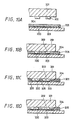
- FIG. 10 and FIG. 11 Such conventional connection members are shown in FIG. 10 and FIG. 11.
- a wiring pattern 203 on the glass substrate 200 and the protrusion electrode 202 of the IC 201 can be electrically connected via conductive particles 205 contained in a connection member 204.
- connection member 204 since there is flatness in each component such as an IC, when the thickness of the connection member 204 (generally, approximately 15 to 25 ⁇ m, incidentally, an ITO (an oxide of indium and tin) pattern wired on the glass is several ⁇ ) is set to the height of the protrusion electrode 202 of the IC 201 plus 5 ⁇ m, the connection member 204 is reliably filled along the lower face of the IC 201. Thus, there is no need to make the thickness of the connection member 204 thicker than the thickness needed, and the conductive particles 205 can be sandwiched between the wiring pattern 203 on the glass substrate 200 and the protrusion electrode 202 of the IC 201 at an early stage of a temporary pressurized attachment (pressurization) in the mounting.
- ITO an oxide of indium and tin
- connection member 204 Even when binder of the connection member 204 flows out at the time of a permanent pressurized attachment (pressurization and heating), the sandwiched conductive particles 205 do not flow, and the wiring pattern 203 on the glass substrate 200 and the protrusion electrode 202 of the IC 201 can be electrically connected reliably via the conductive particles 205 at the time of hardening of the connection member.
- FIG. 10 (A) shows a state where the connection member 204 (for example, an anisotropic conductive film: ACF) is stuck on the glass substrate 200.
- the anisotropic conductive film is stuck on the glass substrate 200 generally by performing thermocompression bonding (pressurization and heating: the amount of pressurization is about 100 N/cm 2 : heating temperature is about 70 to 100°C).
- thermocompression bonding pressurization and heating: the amount of pressurization is about 100 N/cm 2 : heating temperature is about 70 to 100°C.
- FIG. 10 (B) shows a state where the IC 201 is temporarily attached to the glass substrate 200 by pressure.
- the temporary pressurized attachment of the IC 201 is performed only by pressurization or pressurization and heating (heating temperature is about 70 to 100°C).
- FIG. 10 (C) shows a state where the IC 201 is permanently attached to the glass substrate 200 by pressure.
- the permanent pressurized attachment of the IC 201 is performed through pressurization and heating, and since the temperature at that time is higher than the glass transition temperature of the anisotropic conductive film, flow of the binder of the connection member 204 occurs.
- the conductive particles 205 sandwiched between the protrusion electrode 202 of the IC 201 and the wiring pattern 203 on the glass substrate 200 do not flow, however, the conductive particles 205 other than the sandwiched conductive particles 205 flow to the outside.
- FIG. 10 (D) shows a state where the anisotropic conductive film is hardened.
- resin is hardened after the fluidization thereof.
- the series of processes are the connection process.
- the object is not the glass substrate but is instead a printed wiring board 300 as shown in FIG. 11, and when unevenness in height ( ⁇ several ⁇ m) of wiring patterns 303 occurs or when unevenness in height ( ⁇ several ⁇ m) occurs in such a case where the protrusion electrodes 202 of the IC 201 are gold wire bumps, if the thickness of the connection member 204 corresponds to the height (about 20 ⁇ m) of the wiring pattern 303 on the printed wiring board 300 plus the height (about 20 ⁇ m) of the protrusion electrode of the IC, it is necessary to further add 10 to 20 ⁇ m to the thickness of the connection member 204, considering reliability in the connecting.
- connection member 204 since the connection member 204 is thick, the conductive particles 205 cannot be sandwiched between the wiring pattern 303 on the printed wiring board 300 and the protrusion electrode 202 of the IC 201. Thereafter, when the binder of the connection member 204 flows at the time of permanent pressurized attachment (pressurization and heating), the conductive particles 205 also flow similarly, and when the distance between the wiring pattern 303 on the printed wiring board 300 and the protrusion electrode 202 of the IC 201 corresponds to the size of the conductive particle 205, the conductive particles 205 which have flowed are sandwiched during that time. However, the conductive particles 205 do not participate in all connections, and thus electrical connections cannot be obtained. Or since it is necessary to obtain components with strict specifications, the cost increases.
- FIG. 11 (A) shows a state where the connection member 204 (for example, anisotropic conductive film) is stuck on the printed wiring board 300.
- the anisotropic conductive film is stuck on the printed wiring board 300 generally by performing thermocompression bonding (pressurization and heating: the amount of pressurization is about 50 to 100 N/cm 2 : heating temperature is about 50 to 100°C).
- thermocompression bonding pressurization and heating: the amount of pressurization is about 50 to 100 N/cm 2 : heating temperature is about 50 to 100°C).
- FIG. 11 (B) shows a state where the IC 201 is temporarily attached to the printed wiring board 300 by pressure.
- the temporary pressurized attachment of the IC 201 is performed only by pressurization or pressurization and heating (heating temperature is about 70 to 100°C).
- FIG. 11 (C) shows a state where the IC 201 is permanently attached to the printed wiring board 300 by pressure.
- the permanent pressurized attachment of the IC 201 is performed through pressurization and heating, and since the temperature at this time is higher than the glass transition temperature of the anisotropic conductive film, flow of the binder occurs.
- all conductive particles 205 flow as shown by arrows in FIG. 11 (C).
- the conductive particles 205 which have flowed are sandwiched during that time. Therefore, it does not means that the conductive particles 205 exist among all electrodes.
- FIG. 11 (D) shows a state where the anisotropic conductive film is hardened.
- resin is hardened after the fluidization thereof.
- the conductive particles 205 are not sandwiched between the protrusion electrode 202 and the wiring pattern 303, and electrical connection cannot be obtained.
- the present invention was developed considering the above points, and an object of the present invention is to provide electrical connection materials and electrical connection methods by which an electrical connection via conductive particles can be reliably performed regardless of a little unevenness in objects.
- the invention of claim 1 is an electrical connection material for electrically connecting an electrical connection portion of a first object and an electrical connection portion of a second object and is an electrical connection material characterized by being comprised of a first film-like adhesive layer which is a film-like adhesive layer arranged on the first object and is composed of a plurality of conductive particles, a first binder containing the conductive particles, and a first filler and a second film-like adhesive layer which is arranged on the first film-like adhesive layer and is composed of a second binder whose viscosity is lower than that of the first binder and a second filler.
- the first film-like adhesive layer is a film-like adhesive layer arranged on the first object and is composed of a plurality of conductive particles, the first binder containing the conductive particles, and the first filler.
- the second film-like adhesive layer is arranged on the first film-like adhesive layer and is composed of the second binder and the second filler.
- the viscosity of the second binder of the second film-like adhesive layer is set to a value lower than that of the first binder.
- the electrical connection portion of the first object can be electrically connected reliably to the electrical connection portion of the second object, employing the conductive particles of the first film-like adhesive layer.
- the invention of claim 2 is that in the electrical connection material described in claim 1, the conductive particles have an approximately uniform particle diameter.
- the electrical connection portion of the first object and the electrical connection portion of the second object can be electrically connected without rising while having a shape sandwiching the conductive particles reliably.
- the invention of claim 3 is that in the electrical connection material described in claim 1, the material of the second film-like adhesive layer composed of the second binder and the second filler is a binder made of the same material as that of or a material similar to the first binder of the first film-like adhesive layer containing the conductive particles.
- the second film-like adhesive layer is a binder made of the same material as that of or a material similar to the binder of the first film-like adhesive layer, the binders of the first and second film-like adhesive layers react through pressurization and heating so as to glue the first object and the second object.
- the material of the second binder of the second film-like adhesive layer is different from the material of the first binder of the first film-like adhesive layer, after both the binders are hardened while being mixed, inferred is a possibility that a problem of connection reliability occurs.
- the invention of claim 4 is that in the electrical connection material described in claim 1, the viscosity of the second film-like adhesive layer becomes extremely lower than the viscosity of the first film-like adhesive layer in a heating process.
- the viscosity of the second film-like adhesive layer is not necessarily required to be low at room temperature but is required to be extremely lower than that of the first film-like adhesive layer in the process of a thermocompression bonding. On the other hand, when the viscosity of the second film-like adhesive layer is too low at room temperature, a sticking work becomes hard to do.
- the invention of claim 5 is that in the electrical connection material described in claim 1, the thickness of the first film-like adhesive layer containing the conductive particles is set to from approximately the same thickness as the diameter of the conductive particles up to about 4 times the diameter.
- the conductive particles do not protrude from the first film-like adhesive layer containing the conductive particles. That is, the thickness of the first film-like adhesive layer may be a thickness which can be ensured by the conductive particles, and the thickness of the second film-like adhesive layer has to have a thickness by which the second film-like adhesive layer is reliably filled so that voids do not exist between the first object and the second object.
- the invention of claim 6 is that in the electrical connection material described in claim 3, in order that the viscosity of the second film-like adhesive layer composed of the second binder and the second filler is set to a value lower than the viscosity of the first film-like adhesive layer containing the conductive particles, the diameter of the second filler is set to a value larger than the diameter of the first filler.
- the viscosity of the second binder is set to a value lower than the viscosity of the first binder, the second film-like adhesive layer between the first object and the second object flows preferentially by heating and pressurization, and thus the first film-like adhesive layer containing the conductive particles does not move, whereby the position of the conductive particles can be maintained surely.
- the diameter of the second filler particles contained in the second film-like adhesive layer is set to a value larger than the diameter of the first filler particles contained in the first film-like adhesive layer. Since the diameter of the second filler particles is set to a value larger than the diameter of the first filler particles, it is possible that the viscosity of the second film-like adhesive layer containing the second filler particles with a larger diameter is lower and the viscosity of the first film-like adhesive layer containing the first filler particles is higher.
- the invention of claim 7 is that in the electrical connection material described in claim 3, in order that the viscosity of the second film-like adhesive layer composed of the second binder and the second filler is set to a value lower than the viscosity of the first film-like adhesive layer containing the conductive particles, the content by amount of the second filler is set to a value smaller than the content of the first filler.
- the viscosity of the second binder is set to a value lower than the viscosity of the first binder, the second film-like adhesive layer between the first object and the second object flows preferentially by heating and pressurization, and thus the first film-like adhesive layer containing the conductive particles does not move, whereby the position of the conductive particles can be maintained surely.
- the content of the second filler contained in the second film-like adhesive layer is set to a value smaller than the content of the first filler contained in the first film-like adhesive layer. Since the content of the second filler is set to a value smaller than the content of the first filler, it is possible that the viscosity of the second film-like adhesive layer containing the second filler with a small content is lower and the viscosity of the first film-like adhesive layer containing the first filler is higher.
- the invention of claim 8 is that in the electrical connection material described in claim 1, the first filler and the second filler are materials reducing the coefficient of water absorption and the coefficient of linear expansion of a binder.
- the invention of claim 9 is that in the electrical connection material described in claim 1, the electrical connection portion of the first object is a wiring pattern on a circuit substrate, the electrical connection portion of the second object is a protrusion electrode of an electrical component, and the conductive particles in the first film-like adhesive layer containing the conductive particles electrically connect the wiring pattern on the circuit substrate and the protrusion electrode of the electrical component.
- the invention of claim 10 is that in the electrical connection material described in claim 1, the elements of the first binder containing the conductive particles and the second binder of the second film-like adhesive layer are the same or approximately similar.
- the invention of claim 11 is an electrical connection material comprising a first film-like adhesive layer composed of a first binder and a first filler and a second film-like adhesive layer which is composed of a second binder and a second filler and is arranged on the first film-like adhesive layer, characterized in that said first binder is made of a first high molecular resin material and said second binder is made of a second high molecular resin material whose molecular weight is smaller than that of said first high molecular resin material.
- the invention of claim 9 is that in order to make the viscosity of the second film-like adhesive layer lower than that of the first film-like adhesive layer, a high molecular resin material whose molecular weight is smaller than that of the first binder constituting the first film-like adhesive layer is employed as the second binder constituting the second film-like adhesive layer to realize a low viscosity.
- the invention of claim 12 is an electrical connection method for electrically connecting an electrical connection portion of the first object and an electrical connection portion of the second object and is an electrical connection method characterized by comprising an adhesive layer arrangement step for arranging a first film-like adhesive layer which is composed of a plurality of conductive particles, a first binder containing the conductive particles, and a first filler on the electrical connection portion of the first object and a second film-like adhesive layer which is composed of a second binder and a second filler on the first film-like adhesive layer, and a connection step for performing heating and pressurization for electrically connecting the electrical connection portion of the first object and the electrical connection portion of the second object by means of the conductive particles of the first film-like adhesive layer.
- the first film-like adhesive layer is arranged on the electrical connection portion side of the first object, and the second film-like adhesive layer is arranged on the electrical connection portion side of the second object.
- connection step in order to electrically connect the electrical connection portion of the first object and the electrical connection portion of the second object by the conductive particles in the first film-like adhesive layer, heating and pressurization are performed.
- the conductive particles of the first film-like adhesive layer do not move, and only the second film-like adhesive layer flows. Therefore, even when there is a little unevenness of the first object, the first object and the second object can be stuck, and the electrical connection portion of the first object can be electrically connected reliably to the electrical connection portion of the second object, employing the conductive particles of the first film-like adhesive layer.
- connection step comprises a first pressurization heating step for heating and pressurizing the first film-like adhesive layer and the second film-like adhesive layer in a temperature range of ⁇ 20°C centering a temperature at which the viscosity of the second film-like adhesive layer becomes the lowest and a second pressurization heating step for thereafter heating and pressurizing the first film-like adhesive layer and the second film-like adhesive layer at a temperature higher than reaction start temperature of the first film-like adhesive layer and the second film-like adhesive layer.
- the first pressurization heating step is performed where the second film-like adhesive layer is heated and pressurized in a range of ⁇ 20°C centering a temperature at which the viscosity of the second film-like adhesive layer becomes the lowest. Then, at the second pressurization heating step, the first film-like adhesive layer and the second film-like adhesive layer are heated and pressurized at a temperature higher than reaction start temperature of the first film-like adhesive layer and the second film-like adhesive layer.
- the second film-like adhesive layer is fluidized.
- the conductive particles are not fluidized in the first film-like adhesive layer containing the conductive particles, and the conductive particles can be made to exist, for example, between the wiring pattern on the circuit substrate and the protrusion electrode of the electrical component reliably.
- the second pressurization heating step by heating and pressurizing at a temperature higher than the reaction start temperature, the first film-like adhesive layer and the second film-like adhesive layer are completely hardened.
- the invention of claim 14 is that in the electrical connection method described in claim 13, even in a temperature range of ⁇ 20°C centering a temperature at which the viscosity of the first film-like adhesive layer containing the conductive particles and the viscosity of the second film-like adhesive layer become the lowest, the viscosity of the first film-like adhesive layer containing the conductive particles is higher than the viscosity of the second film-like adhesive layer, therefore the second film-like adhesive layer is fluidized.
- the conductive particles of the first film-like adhesive layer containing the conductive particles is not fluidized, and the conductive particles in the first film-like adhesive layer containing the conductive particles are made to exist between the wiring pattern on the circuit substrate and the protrusion electrode of the electrical component to electrically connect the wiring pattern and the protrusion electrode.
- the invention of claim 15 is that in the electrical connection method described in claim 13, the becoming-lowest-temperature is 80°C.
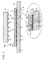
- FIG. 1 shows one example of an electrical device 150 electrically connected according to a preferred embodiment of an electrical connection material 100 of the present invention.
- This electrical device 150 is provided with a printed wiring board 4 and an IC (integrated circuit) 2 as an example of an electrical component.
- a wiring pattern 5 in a shape of a predetermined pattern is formed on one face 4A of the printed wiring board 4.
- This wiring pattern 5 is an electrical wiring pattern formed, for example, by aluminum and copper.
- a plurality of protrusion electrodes 3 are provided, for example, on one face 2A. These protrusion electrodes 3 are also called bumps, and the protrusion electrodes 3 are, for example, arranged while being protruded corresponding to the wiring pattern 5 on the printed wiring board 4.
- the printed wiring board 4 corresponds to a first object
- the wiring pattern 5 on the printed wiring board 4 corresponds to a wiring pattern on a circuit substrate.
- the IC 2 is an electrical component corresponding to a second object.
- the electrical connection material 100 has a function for electrically connecting the wiring pattern 5 on the printed wiring board 4 and the protrusion electrodes 3 of the IC 2 and for mechanically gluing the printed wiring board 4 and the IC 2 reliably.
- the electrical connection material 100 has a first film-like adhesive layer 6 and a second film-like adhesive layer 9.
- the first film-like adhesive layer 6 contains a first binder 8, conductive particles 7, and a first filler F1.
- the second film-like adhesive layer 9 is composed of a second binder 9A and a second filler F2.
- the first film-like adhesive layer 6 containing the conductive particles 7 is of a film-like object arranged on the face 4A of the printed wiring board 4, and the first film-like adhesive layer 6 is stuck on the face 4A of the printed wiring board 4 so as to cover the wiring pattern 5.
- the conductive particles 7 and the first filler particles F1 in the first film-like adhesive layer 6 are contained so as to be dispersed approximately uniformly in the first binder 8.
- the conductive particles 7, for example, are particles formed by plating of Ni (300 to 1000 ⁇ thickness) on plastic resin particles (diameter 5 ⁇ m) and further plating of Au (300 to 1000 ⁇ thickness) thereon or are globular particles formed of metal powder of Ni (5 to 10 ⁇ m diameter).
- the diameter of the first filler particles F1 which is smaller than or the same as that of the conductive particles 7 is preferable.
- the first filler F1 by selecting a material which can reduce the coefficient of water absorption and/or the coefficient of linear expansion of the binder and/or can give electrical insulation property, the reliability of the electrical connection between a wiring pattern on a circuit substrate and a protrusion electrode of an electrical component can be improved. That is, when the water absorption coefficient of the binder is reduced, occurrence of package crack due to moisture absorption of an adhesive layer can be restrained, for example, in a production process accompanied by a reflow furnace.
- silica or the like is preferable as the material of the first filler F1 which has an effect for that improvement.
- the first binder 8 is a binder to contain a plurality or many conductive particles 7 and the first filler particles F1 and is further to retain them so that they are not moved.
- the first binder 8 is, for example, formed of a thermosetting epoxy resin which has electrical isolation property.
- the thickness D of the first binder 8 is set to from the same thickness as the diameter d of the conductive particle 7 up to about 4 times the diameter d.
- the conductive particles 7 are completely contained and retained in the first binder 8 without protruding to the outside of the first binder 8 which is an electrical isolation layer.
- the conductive particles 7 are preferably ranged in line or are dispersed uniformly in the first binder 8 as shown in FIG. 1.
- the first filler particles F1 are also dispersed uniformly in the first binder 8.
- the second film-like adhesive layer 9 composed of the second binder 9A and the second filler F2 in FIG. 1 is arranged on the first film-like adhesive layer 6 and is combined therewith to form a two-layer structure.
- the second film-like adhesive layer 9 is provided with the second binder 9A and the second filler F2. Many or a plurality of the second filler particles F2 are contained in the second binder 9A while being ranged in line or dispersed uniformly.
- the second binder 9A in the second film-like adhesive layer 9 an adhesive material which contains the same element as the material of the first binder 8 and has an electrical isolation property can be adopted.
- the first binder 8 in the first film-like adhesive layer 6 is, for example, formed of a thermosetting epoxy resin.
- a binder of the same reactivity preferably by which the same reaction is occurred at the time of pressurization and heating can be adopted.
- the viscosity of the second film-like adhesive layer 9 is set to a value lower than the viscosity of the first film-like adhesive layer 6. That is, the second film-like adhesive layer 9 has a higher fluidity compared with the first film-like adhesive layer 6 containing the conductive particles 7, and when the IC 2 is pressed on the face 4A of the printed wiring board 4 via the electrical connection material 100, only the second film-like adhesive layer 9 can flow and fill up between the first film-like adhesive layer 6 containing the conductive particles 7 and the face 2A of the IC 2.
- the second filler particles F2 contained in the second film-like adhesive layer 9 which have a larger diameter than that of the first filler particles F1 contained in the first film-like adhesive layer 6 containing the conductive particles 7 are employed.
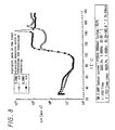
- FIG. 8 shows an example of viscosity data of the first film-like adhesive layer 6 containing the conductive particles 7.
- FIG. 9 shows an example of viscosity data of the second film-like adhesive layer 9 composed of the second binder 9A and the second filler F2.
- the viscosity of the first film-like adhesive layer 6 containing the conductive particles and the viscosity data of the second film-like adhesive layer 9 is higher at any temperature than that of the second film-like adhesive layer 9.
- the overall viscosity from the viscosity data of the second film-like adhesive layer 9 in FIG. 9 is lower than that from the temperature data of the first film-like adhesive layer 6 in FIG. 8. From this view point, it can be said that the fluidity of the second film-like adhesive layer 9 is higher than that of the first film-like adhesive layer 6.
- first binder 8 and the second binder 9A for example; bisphenol type epoxy resin, modified epoxy resin, amino hardening agent, phenoxy resin, and the like can be employed, however, as other examples, low molecular bisphenol type epoxy resin is employed as the second binder 9A and high molecular bisphenol type epoxy resin is employed as the first binder 8 so that a difference in the viscosity can be obtained.
- connection method by which the IC 2 is electrically connected to the printed wiring board 4, employing the electrical connection material 100, is explained referring to FIG. 2 to FIG. 6.
- FIG. 2 to FIG. 5 sequentially show the method of electrical connection employing the electrical connection material 100
- FIG. 6 is a flow chart showing the electrical connection method.
- the first film-like adhesive layer 6 containing the conductive particles 7 is stuck on the face 4A of the printed wiring board 4 as shown in FIG. 1 and FIG. 2.
- the first film-like adhesive layer 6 is stuck so as to cover the wiring pattern 5.
- the conductive particles 7 are completely contained and are retained in the first binder 8. This is because the thickness of the first binder 8 is from the same as the diameter of the conductive particle 7 up to about 4 times the diameter.
- the second film-like adhesive layer 9 is arranged on the first film-like adhesive layer 6 to form a two-layer structure of the first film-like adhesive layer 6 and the second film-like adhesive layer 9.
- the IC 2 is positioned toward the printed wiring board 4 as shown in FIG. 1 and FIG. 2. That is, the protrusion electrode 3 of the IC 2 is positioned at a position corresponding to the wiring pattern 5.
- Connection step S3 in FIG. 6 includes first pressurization heating step S4 and second pressurization heating step S5.
- the IC 2 is placed on the first film-like adhesive layer 6 containing the conductive particles 7 so that the second film-like adhesive layer 9 flows and spreads, and the first film-like adhesive layer 6 containing the conductive particles 7 retains the shape thereof as shown in FIG. 3.
- the second film-like adhesive layer 9 is filled between the face 2A of the IC 2 and the first film-like adhesive layer 6 as shown in FIG. 3. This is because the viscosity of the second film-like adhesive layer 9 is lower than that of the first film-like adhesive layer 6, only the second film-like adhesive layer 9 spreads to the vicinity thereof so that the second film-like adhesive layer 9 is filled between the face 2A of the IC 2 and the first film-like adhesive layer 6. In the state of FIG. 3, the second film-like adhesive layer 9 is only temporarily hardened.
- the temperature at this time is a temperature at which the viscosity of the second film-like adhesive layer 9 composed of the second binder 9A and the second filler F2 becomes the lowest or is in a temperature range thereabout.
- the temperature at which the viscosity of the second film-like adhesive layer 9 becomes the lowest is 80°C, and since electrical connection reliability is excellent in a temperature range of ⁇ 20°C of the vicinity centering 80°C, heating and pressurization is performed in the temperature range of 60 to 100°C.
- the temperature of the heating time is, for example, 80°C
- the heating time is, for example, about 5 seconds.
- the pressure at that time is about a pressure or less by which the conductive particles 7 existing between the wiring pattern 5 on the printed wiring board 4 and the protrusion electrode 3 of the IC 2 are transformed, for example, 2 ⁇ m or more after the second pressurization heating step S5 and that is, for example, 10 Kgf/mm 2 (100 Pa) for the area of the face of the protrusion electrode 3 of the IC 2 connected to the wiring pattern 5 on the printed wiring board 4 via the conductive particles 7 is imparted while heating.
- the pressure is given as much as that by which the conductive particles 7 existing between the wiring pattern 5 on the printed wiring board 4 and the protrusion electrode 3 of the IC 2 can be transformed, for example, 2 ⁇ m or more after the second pressurization heating step S5, and the first binder 8 and the second film-like adhesive layer 9 are heated at a higher temperature.
- the temperature at this time is a temperature higher than reaction start temperature of the first binder 8 and the second film-like adhesive layer 9, for example, 180°C to 230°C, and heating is performed at this temperature for 20 seconds to 30 seconds.
- the pressure at that time to be given is, for example, about 10 to 15 Kgf/mm 2 (150 Pa) for the area of the face of the protrusion electrode 3 of the IC 2 connected to the wiring pattern 5 on the printed wiring board 4 via the conductive particles 7. Since being preferably the same or similar element, the first binder 8 of the first film-like adhesive layer 6 and the second binder 9A of the second film-like adhesive layer 9 can be hardened approximately at the same time.
- each protrusion electrode 3 can be connected electrically reliably with the wiring pattern 5, employing the conductive particles 7 of the first film-like adhesive layer 6 containing the conductive particles 7.
- the conductive particles 7 are positioned so as to be sandwiched between the protrusion electrode 3 and the wiring pattern 5.
- FIG. 4 when pressurization whose amount is similar or stronger than that in the first pressurization heating step S4 is performed, only the conductive particles 7 positioned between the protrusion electrode 3 and the wiring pattern 5 are electrically connected while being sandwiched between the protrusion electrode 3 and the wiring pattern 5, and conductive particles 7 other than sandwiched conductive particles move to the vicinity thereof to some extent.
- the diameter of the second filler particles F2 contained in the second film-like adhesive layer 9 is, for example, 1.8 ⁇ m on average and 8 ⁇ m at the maximum, and the second filler F2 flows at the first pressurization heating step S4.
- the diameter of the conductive particle 7 contained in the first film-like adhesive layer 6 is, for example, 5 ⁇ m, and the diameter of the the first filler particles F1 is 1.2 ⁇ m on average and 5 ⁇ m or less at the maximum.
- the thickness of the film-like adhesive layer containing conductive particles is set to from about the same thickness as the diameter of the conductive particles up to about 4 times the diameter, and thus the conductive particles 7 are not exposed from and fallen away from the first binder 8, and the conductive particles 7 are more reliably sandwiched between the protrusion electrode 3 of the IC 2 and the wiring pattern 5 formed on the printed wiring board 4.
- the viscosity of the first film-like adhesive layer 6 containing the conductive particles 7 is made higher and the viscosity of the second film-like adhesive layer 9 composed of the second binder and the second filler is made lower, the second film-like adhesive layer 9 composed of the second binder and the second filler easily flows at the time of heating and pressurization, whereby the conductive particles 7 are reliably sandwiched between the protrusion electrode 3 of the IC and the wiring pattern 5 formed on the printed wiring board 4.
- the diameter of the second filler particles F2 contained in the second film-like adhesive layer 9 is made larger than that of the first filler particles F1 contained in the first film-like adhesive layer 6 containing the conductive particles 7.
- fillers contained in the adhesive layers by selecting a material by which the water absorption coefficient and/or the linear expansion coefficient of an adhesive layer can be reduced, electrical connection reliability of a wiring pattern on a circuit substrate and a protrusion electrode of an electrical component can be improved.
- a material having the effect for that purpose is, for example, ceramics such as silica and alumina typically.
- the elements of the first binder 8 in the first film-like adhesive layer 6 containing the conductive particles 7 and the elements of the second binder 9A of the second film-like adhesive layer 9 are the same or approximately similar, at the time of heating and flowing, even when the first binder 8 and the second film-like adhesive layer 9 composed of the second binder 9A and the second filler F2 are mixed, the mixing does not exert a bad influence on the connection reliability.
- the first film-like adhesive layer 6 containing the conductive particles 7 when the viscosity of the first film-like adhesive layer 6 containing the conductive particles 7 is higher than that of the second film-like adhesive layer 9, the first film-like adhesive layer 6 containing the conductive particles 7 can maintain the film shape thereof at the temperature and in a range of the vicinity of that temperature ( ⁇ 20°C) at which the viscosity of the first film-like adhesive layer 6 containing the conductive particles 7 and the viscosity of the second film-like adhesive layer 9 become the lowest, whereby the conductive particles 7 can be reliably sandwiched between the protrusion electrode 3 of the IC 2 and the wiring pattern 5 formed on the printed wiring board 4.
- an electrical connection member and an electrical connection method through which an electrical connection via the conductive particles 7 can be achieved can be realized.
- the conductive particles 7 are made to exist between a protrusion electrode of an electrical component such as a bare chip and a conductive pattern of an object, and an electrical connection can be reliably obtained.
- Performed is positioning of the first film-like adhesive layer 6 whose thickness is set to from approximately the same as the diameter of the conductive particles up to about 4 times the diameter of the conductive particles and the second film-like adhesive layer 9 which is arranged over the first film-like adhesive layer 6 and is formed of a binder with the same reactivity as that of an element of the binder of the first film-like adhesive layer 6 so that the wiring pattern of the object and the protrusion electrode of the IC correspond to each other, and after pressurization, the electrical connection is performed reliably through heating and pressurization.
- the second pressurization heating step is performed where the first binder 8 of the first film-like adhesive layer 6 and the second binder 9A of the second film-like adhesive layer 9 are heated at a temperature higher than the reaction start temperature of the first binder 8 and the second binder 9A so that both adhesive layers can be efficiently hardened.
- the thickness of the first film-like adhesive layer 6 with conductivity is set to from about the same thickness as the diameter of the conductive particle 7 up to about 4 times the diameter of the conductive particle 7.
- the conductive particles do not protrude from the film-like adhesive layer containing the conductive particles.
- the conductive particles have approximately uniform particle diameter
- the material of the film-like binder composed of a binder and a filler is the same as that of the binder of the film-like binder containing the conductive particles or is a similar material.
- the binder of the two-layer film-like adhesive layer reacts through pressurization and heating so that the first object and the second object can be connected. Since the conductive particles have an approximately uniform particle diameter, the electrical connection portion of the first object and the electrical connection portion of the second object can be electrically connected without rising while having a shape sandwiching the conductive particles reliably.
- the material of the second binder of the second film-like adhesive layer is different from the material of the first binder of the first film-like adhesive layer, after both the binders are hardened while being mixed, inferred is a possibility that a problem of connection reliability occurs.
- the viscosity of the second film-like adhesive layer is made to become extremely lower than the viscosity of the first film-like adhesive layer preferably in the heating process.
- the viscosity of the second film-like adhesive layer is not always required to be low at a room temperature, and it is necessary for the viscosity of the second film-like adhesive layer to be extremely lower than that of the first film-like adhesive layer in the process of the thermocompression bonding. On the other hand, when the viscosity of the second film-like adhesive layer is too low at a room temperature, sticking work becomes hard to do.
- the thickness of the first film-like adhesive layer may be a thickness which can be ensured by the conductive particles, and the thickness of the second film-like adhesive layer has to have a thickness with which the second film-like adhesive layer is reliably filled so that voids do not exist between the first object and the second object.
- the viscosity of the second binder is set to a value lower than that of the first binder, the second film-like adhesive layer between the first object and the second object flows preferentially by heating and pressurization, and thus the first film-like adhesive layer containing the conductive particles does not move, whereby the position of the conductive particles can be maintained surely.
- the content by amount of the second filler contained in the second film-like adhesive layer is set to a value smaller than that of the first filler contained in the first film-like adhesive layer. Since the content of the second filler is set to a content smaller than the content of the first filler, it is possible to make the viscosity of the second film-like adhesive layer having the second filler whose content is small lower and the viscosity of the first film-like adhesive layer containing the first filler higher.
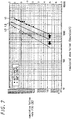
- FIG. 7 shows an example that is a measurement result of fraction defective with respect to time elapse, that is, an example of reinforcement of electrical connection reliability by employing electrical connection materials when an electrical connection is performed employing the electrical connection material of the present invention.
- Straight line L1 in FIG. 7 shows an example in which the printed wiring board 4 and the IC 2 in FIG. 1 are temporarily attached by pressure, for example, at 80°C and are permanently attached by pressure at 210°C.
- Straight line L2 in FIG. 7 shows an example in which the printed wiring board 4 and the IC 2 are temporarily attached by pressure, for example, at 130°C and are permanently attached by pressure at 210°C.
- Straight line L3 is the result at the time when the printed wiring board and the IC 2 are constantly heated at 210°C.
- the straight line L1 and the straight line L2 exist in the opposite sides sandwiching the straight line L3, and the straight line L1 can maintain electrical connection reliability for a long time as compared with the case of the straight line L2. That is, the straight line L1 has a high electrical connection reliability, however, electrical connection reliability is deteriorated in the case of the straight line L2. This means that since a difference does not occur in the viscosities of the first film-like adhesive layer and the second film-like adhesive layer at 130°C (refer to FIG. 8 and FIG. 9), reliable connection of conductive particles is not possible. Further, half-finished hardening of a binder progresses, and hardening in an ideal hardening state is not possible at the permanent pressurized attachment thereafter (210°C). As a result, connection reliability in the case of the straight line L2 is worsened than in the case of the straight line L3 that is a result data of constant heating.
- the present invention is not limited to the embodiment described above.
- the first object is the printed wiring board 4 having the wiring pattern 5 and the second object is the IC 2 having the protrusion electrode 3, others can be adopted for each one.
- the first object instead of the printed wiring board 4, another kind such as a glass substrate having the wiring pattern 5 can also be adopted.
- the second object instead of the IC 2, a different feature of electrical component can also be adopted.
- the shape of the protrusion electrode 3 one such as a plated bump can be adopted.
- the shape of the conductive particle 7 is not limited to being globular, and other shapes can also be adopted.
Landscapes
- Engineering & Computer Science (AREA)
- Manufacturing & Machinery (AREA)
- Microelectronics & Electronic Packaging (AREA)
- Adhesives Or Adhesive Processes (AREA)
- Wire Bonding (AREA)
- Conductive Materials (AREA)
- Manufacturing Of Electrical Connectors (AREA)
Abstract
Description
Claims (15)
- An electrical connection material for electrically connecting an electrical connection portion of a first object and an electrical connection portion of a second object, characterized in that the electrical connection material comprisesa first film-like adhesive layer which is a film-like adhesive layer arranged on said first object and is composed of a plurality of conductive particles, a first binder containing the conductive particles, and a first filler anda second film-like adhesive layer which is arranged on said first film-like adhesive layer and is composed of a second binder whose viscosity is lower than that of said first binder and a second filler.
- The electrical connection material according to claim 1, characterized in thatsaid conductive particles have an approximately uniform particle diameter.
- The electrical connection material according to claim 1, characterized in thatthe material of said second film-like adhesive layer composed of said second binder and said second filler is a binder having the same material as that of or a material similar to said first binder of said first film-like adhesive layer containing said conductive particles.
- The electrical connection material according to claim 1, characterized in thatthe viscosity of said second film-like adhesive layer becomes extremely lower than the viscosity of said first film-like adhesive layer in a heating process.
- The electrical connection material according to claim 1, characterized in thatthe thickness of said first film-like adhesive layer containing said conductive particles is set to from approximately the same thickness as the diameter of said conductive particles up to about 4 times the diameter.
- The electrical connection material according to claim 3, characterized in thatin order that the viscosity of said second film-like adhesive layer composed of said second binder and said second filler is set to a value lower than the viscosity of said first film-like adhesive layer containing said conductive particles, the diameter of said second filler particles is set to a value larger than the diameter of said first filler particles.
- The electrical connection material according to claim 3, characterized in thatin order that the viscosity of said second film-like adhesive layer composed of said second binder and said second filler is set to a value lower than the viscosity of said first film-like adhesive layer containing said conductive particles, the content by amount of said second filler is set to a value smaller than the content of said first filler.
- The electrical connection material according to claim 1, characterized in thatsaid first filler and said second filler are materials reducing the coefficient of water absorption and the coefficient of linear expansion of a binder.
- The electrical connection material according to claim 1, characterized in thatthe electrical connection portion of said first object is a wiring pattern on a circuit substrate, the electrical connection portion of said second object is a protrusion electrode of an electrical component, and said conductive particles in said first film-like adhesive layer containing said conductive particles electrically connect the wiring pattern on said circuit substrate and the protrusion electrode of said electrical component.
- The electrical connection material according to claim 1, characterized in thatthe elements of said first binder containing said conductive particles and said second binder of said second film-like adhesive layer are the same or approximately similar.
- An electrical connection material comprising a first film-like adhesive layer composed of a first binder and a first filler anda second film-like adhesive layer which is composed of a second binder and a second filler and is arranged on said first film-like adhesive layer, characterized in that said first binder is made of a first high molecular resin material and said second binder is made of a second high molecular resin material whose molecular weight is smaller than that of said first high molecular resin material.
- An electrical connection method for electrically connecting an electrical connection portion of a first object and an electrical connection portion of a second object, characterized in that the electrical connection method comprisesan adhesive layer arrangement step for arranging a first film-like adhesive layer which is composed of a plurality of conductive particles, a first binder containing said conductive particles, and a first filler on the electrical connection portion of said first object and a second film-like adhesive layer which is composed of a second binder and a second filler on said first film-like adhesive layer anda connection step for performing heating and pressurization for electrically connecting the electrical connection portion of said first object and the electrical connection portion of said second object by means of said conductive particles of said first film-like adhesive layer.
- The electrical connection method according to claim 12, characterized in that said connection step comprisesa first pressurization heating step for heating and pressurizing said first film-like adhesive layer and said second film-like adhesive layer in a temperature range of ±20°C centering a temperature at which the viscosity of said second film-like adhesive layer becomes the lowest anda second pressurization heating step for thereafter heating and pressurizing said first film-like adhesive layer and said second film-like adhesive layer at a temperature higher than reaction start temperature of said first film-like adhesive layer and said second film-like adhesive layer.
- The electrical connection method according to claim 13, characterized in thateven in a temperature range of ±20°C centering a temperature at which the viscosity of said second film-like adhesive layer becomes the lowest, the viscosity of said first film-like adhesive layer containing said conductive particles is higher than the viscosity of said second film-like adhesive layer, said second film-like adhesive layer is fluidized, said conductive particles of said first film-like adhesive layer containing said conductive particles is not fluidized, and said conductive particles in said first film-like adhesive layer containing said conductive particles are made to exist between a wiring pattern on a circuit substrate and a protrusion electrode of an electrical component to electrically connect the wiring pattern and the protrusion electrode.
- The electrical connection method according to claim 13, characterized in thatthe temperature at which the viscosity of said second film-like adhesive layer becomes the lowest is 80°C.
Applications Claiming Priority (3)
| Application Number | Priority Date | Filing Date | Title |
|---|---|---|---|
| JP2000087104 | 2000-03-23 | ||
| JP2000087104 | 2000-03-23 | ||
| PCT/JP2001/002356 WO2001071854A1 (en) | 2000-03-23 | 2001-03-23 | Electrical connection material and electrical connection method |
Publications (3)
| Publication Number | Publication Date |
|---|---|
| EP1189308A1 true EP1189308A1 (en) | 2002-03-20 |
| EP1189308A4 EP1189308A4 (en) | 2005-06-08 |
| EP1189308B1 EP1189308B1 (en) | 2007-03-07 |
Family
ID=18603168
Family Applications (1)
| Application Number | Title | Priority Date | Filing Date |
|---|---|---|---|
| EP01915737A Expired - Lifetime EP1189308B1 (en) | 2000-03-23 | 2001-03-23 | Electrical connection material and electrical connection method |
Country Status (6)
| Country | Link |
|---|---|
| EP (1) | EP1189308B1 (en) |
| JP (1) | JP4411819B2 (en) |
| KR (1) | KR100738246B1 (en) |
| DE (1) | DE60127056T2 (en) |
| TW (1) | TW492215B (en) |
| WO (1) | WO2001071854A1 (en) |
Cited By (1)
| Publication number | Priority date | Publication date | Assignee | Title |
|---|---|---|---|---|
| CN102334182A (en) * | 2009-02-27 | 2012-01-25 | 索尼化学&信息部件株式会社 | Manufacturing method of semiconductor device |
Families Citing this family (8)
| Publication number | Priority date | Publication date | Assignee | Title |
|---|---|---|---|---|
| KR100684169B1 (en) * | 2005-08-11 | 2007-02-20 | 삼성전자주식회사 | Adhesive film having a binary filler distribution and its manufacturing method, chip lamination package using the same and manufacturing method |
| JP5311772B2 (en) | 2007-06-27 | 2013-10-09 | デクセリアルズ株式会社 | Adhesive film |
| JP5226562B2 (en) * | 2008-03-27 | 2013-07-03 | デクセリアルズ株式会社 | Anisotropic conductive film, joined body and method for producing the same |
| JP4623224B2 (en) * | 2008-06-26 | 2011-02-02 | 日立化成工業株式会社 | Resin film sheet and electronic parts |
| JP5540916B2 (en) * | 2010-06-15 | 2014-07-02 | デクセリアルズ株式会社 | Method for manufacturing connection structure |
| JP5631654B2 (en) * | 2010-07-28 | 2014-11-26 | デクセリアルズ株式会社 | Manufacturing method and connection method of mounting body |
| WO2015056754A1 (en) * | 2013-10-17 | 2015-04-23 | デクセリアルズ株式会社 | Anisotropic conductive adhesive and connection structure |
| JP6307308B2 (en) * | 2014-03-06 | 2018-04-04 | デクセリアルズ株式会社 | Manufacturing method of connection structure and circuit connection material |
Family Cites Families (11)
| Publication number | Priority date | Publication date | Assignee | Title |
|---|---|---|---|---|
| US4554033A (en) * | 1984-10-04 | 1985-11-19 | Amp Incorporated | Method of forming an electrical interconnection means |
| US4643843A (en) * | 1985-06-03 | 1987-02-17 | Lowdon Harold L | Preparation for improving the reliability of electrical connections |
| JPS6215777A (en) * | 1985-07-12 | 1987-01-24 | 日本写真印刷株式会社 | Film-like connector and manufacture thereof |
| JPH0770252B2 (en) * | 1988-01-28 | 1995-07-31 | 信越ポリマー株式会社 | Thermal adhesive flexible wiring member |
| US5371327A (en) * | 1992-02-19 | 1994-12-06 | Shin-Etsu Polymer Co., Ltd. | Heat-sealable connector sheet |
| JP2888466B2 (en) * | 1992-04-07 | 1999-05-10 | 信越ポリマー株式会社 | Manufacturing method of heat seal connector |
| JPH0685337B2 (en) * | 1992-10-30 | 1994-10-26 | 信越ポリマー株式会社 | Heat seal connector |
| EP0692137B1 (en) * | 1994-01-27 | 2002-04-10 | Loctite (Ireland) Limited | Compositions and methods for providing anisotropic conductive pathways and bonds between two sets of conductors |
| JPH08279388A (en) * | 1995-04-04 | 1996-10-22 | Idemitsu Kosan Co Ltd | How to connect electrical circuits |
| JP2710234B2 (en) * | 1995-07-31 | 1998-02-10 | 日本電気株式会社 | Terminal connection method and circuit board manufactured by this method |
| JP3258550B2 (en) * | 1996-01-12 | 2002-02-18 | 日本黒鉛工業株式会社 | Three-layer conductive anisotropic strip for fine pitch heat seal connector and method of manufacturing the same |
-
2001
- 2001-03-23 TW TW090106949A patent/TW492215B/en not_active IP Right Cessation
- 2001-03-23 KR KR1020017015002A patent/KR100738246B1/en not_active Expired - Fee Related
- 2001-03-23 JP JP2001569929A patent/JP4411819B2/en not_active Expired - Fee Related
- 2001-03-23 EP EP01915737A patent/EP1189308B1/en not_active Expired - Lifetime
- 2001-03-23 WO PCT/JP2001/002356 patent/WO2001071854A1/en not_active Ceased
- 2001-03-23 DE DE60127056T patent/DE60127056T2/en not_active Expired - Lifetime
Cited By (5)
| Publication number | Priority date | Publication date | Assignee | Title |
|---|---|---|---|---|
| CN102334182A (en) * | 2009-02-27 | 2012-01-25 | 索尼化学&信息部件株式会社 | Manufacturing method of semiconductor device |
| EP2402985A4 (en) * | 2009-02-27 | 2014-01-22 | Sony Chem & Inf Device Corp | METHOD FOR MANUFACTURING SEMICONDUCTOR DEVICE |
| CN102334182B (en) * | 2009-02-27 | 2015-11-25 | 迪睿合电子材料有限公司 | Manufacturing method of semiconductor device |
| US9368374B2 (en) | 2009-02-27 | 2016-06-14 | Dexerials Corporation | Method of manufacturing semiconductor device |
| US9524949B2 (en) | 2009-02-27 | 2016-12-20 | Dexerials Corporation | Semiconductor device having semiconductor chip affixed to substrate via insulating resin adhesive film |
Also Published As
| Publication number | Publication date |
|---|---|
| KR100738246B1 (en) | 2007-07-12 |
| EP1189308A4 (en) | 2005-06-08 |
| DE60127056T2 (en) | 2007-11-08 |
| TW492215B (en) | 2002-06-21 |
| WO2001071854A1 (en) | 2001-09-27 |
| DE60127056D1 (en) | 2007-04-19 |
| JP4411819B2 (en) | 2010-02-10 |
| KR20020022676A (en) | 2002-03-27 |
| EP1189308B1 (en) | 2007-03-07 |
Similar Documents
| Publication | Publication Date | Title |
|---|---|---|
| US7078807B2 (en) | Electrical connection materials and electrical connection methods | |
| US6034331A (en) | Connection sheet and electrode connection structure for electrically interconnecting electrodes facing each other, and method using the connection sheet | |
| TW523885B (en) | Manufacturing method of electric device | |
| KR100563890B1 (en) | Electrical connecting device and electrical connecting method | |
| TWI379624B (en) | Printed circuit board and method of producing the same | |
| KR100701133B1 (en) | Electrical connection device and electrical connection method | |
| EP1189308B1 (en) | Electrical connection material and electrical connection method | |
| US6528889B1 (en) | Electronic circuit device having adhesion-reinforcing pattern on a circuit board for flip-chip mounting an IC chip | |
| JP3436170B2 (en) | Anisotropic conductive film, semiconductor device using the same, and method of manufacturing the same | |
| JPWO2001071854A1 (en) | Electrical connection material and electrical connection method | |
| JP2004342766A (en) | Circuit board and electronic component package | |
| JP2004006417A (en) | Connecting element and connection structure of electrode using this | |
| JP4378788B2 (en) | IC chip connection method | |
| US20100123258A1 (en) | Low Temperature Board Level Assembly Using Anisotropically Conductive Materials | |
| JP2006339160A (en) | Thermosetting circuit connection member, electrode connection structure using the same, and electrode connection method | |
| JP2001307555A (en) | Anisotropic conductive film, mounting method using the same, and wiring substrate | |
| JP4595981B2 (en) | Connection member, electrode connection structure and connection method using the connection member | |
| JP3704497B2 (en) | Circuit board, repair method and mounting structure | |
| JP4595980B2 (en) | Connection member, electrode connection structure and connection method using the connection member | |
| JP2000100865A (en) | Semiconductor device and method of manufacturing the same | |
| JP4631889B2 (en) | Connection member, electrode connection structure and connection method using the connection member | |
| JP2008060084A (en) | Connecting member, and connection structure and connecting method of electrode using the connecting member | |
| EP4075485A1 (en) | Method for manufacturing electronic component | |
| JP2007141914A (en) | Connection method between printed circuit boards | |
| US20030070836A1 (en) | PGA chip package and process for same |
Legal Events
| Date | Code | Title | Description |
|---|---|---|---|
| PUAI | Public reference made under article 153(3) epc to a published international application that has entered the european phase |
Free format text: ORIGINAL CODE: 0009012 |
|
| 17P | Request for examination filed |
Effective date: 20011205 |
|
| AK | Designated contracting states |
Kind code of ref document: A1 Designated state(s): AT BE CH CY DE DK ES FI FR GB GR IE IT LI LU MC NL PT SE TR |
|
| RBV | Designated contracting states (corrected) |
Designated state(s): DE FI FR |
|
| A4 | Supplementary search report drawn up and despatched |
Effective date: 20050426 |
|
| 17Q | First examination report despatched |
Effective date: 20050630 |
|
| GRAP | Despatch of communication of intention to grant a patent |
Free format text: ORIGINAL CODE: EPIDOSNIGR1 |
|
| GRAS | Grant fee paid |
Free format text: ORIGINAL CODE: EPIDOSNIGR3 |
|
| GRAA | (expected) grant |
Free format text: ORIGINAL CODE: 0009210 |
|
| AK | Designated contracting states |
Kind code of ref document: B1 Designated state(s): DE FI FR |
|
| REF | Corresponds to: |
Ref document number: 60127056 Country of ref document: DE Date of ref document: 20070419 Kind code of ref document: P |
|
| PLBE | No opposition filed within time limit |
Free format text: ORIGINAL CODE: 0009261 |
|
| STAA | Information on the status of an ep patent application or granted ep patent |
Free format text: STATUS: NO OPPOSITION FILED WITHIN TIME LIMIT |
|
| 26N | No opposition filed |
Effective date: 20071210 |
|
| PGFP | Annual fee paid to national office [announced via postgrant information from national office to epo] |
Ref country code: FI Payment date: 20110314 Year of fee payment: 11 Ref country code: FR Payment date: 20110404 Year of fee payment: 11 |
|
| PGFP | Annual fee paid to national office [announced via postgrant information from national office to epo] |
Ref country code: DE Payment date: 20110325 Year of fee payment: 11 |
|
| PG25 | Lapsed in a contracting state [announced via postgrant information from national office to epo] |
Ref country code: FI Free format text: LAPSE BECAUSE OF NON-PAYMENT OF DUE FEES Effective date: 20120323 |
|
| REG | Reference to a national code |
Ref country code: FR Ref legal event code: ST Effective date: 20121130 |
|
| REG | Reference to a national code |
Ref country code: DE Ref legal event code: R119 Ref document number: 60127056 Country of ref document: DE Effective date: 20121002 |
|
| PG25 | Lapsed in a contracting state [announced via postgrant information from national office to epo] |
Ref country code: FR Free format text: LAPSE BECAUSE OF NON-PAYMENT OF DUE FEES Effective date: 20120402 |
|
| PG25 | Lapsed in a contracting state [announced via postgrant information from national office to epo] |
Ref country code: DE Free format text: LAPSE BECAUSE OF NON-PAYMENT OF DUE FEES Effective date: 20121002 |