EP1189285A1 - Production method for bonding wafer and bonding wafer produced by this method - Google Patents
Production method for bonding wafer and bonding wafer produced by this method Download PDFInfo
- Publication number
- EP1189285A1 EP1189285A1 EP01914187A EP01914187A EP1189285A1 EP 1189285 A1 EP1189285 A1 EP 1189285A1 EP 01914187 A EP01914187 A EP 01914187A EP 01914187 A EP01914187 A EP 01914187A EP 1189285 A1 EP1189285 A1 EP 1189285A1
- Authority
- EP
- European Patent Office
- Prior art keywords
- wafer
- bonded
- temperature
- ion implantation
- delamination
- Prior art date
- Legal status (The legal status is an assumption and is not a legal conclusion. Google has not performed a legal analysis and makes no representation as to the accuracy of the status listed.)
- Withdrawn
Links
Images

Classifications
-
- H—ELECTRICITY
- H10—SEMICONDUCTOR DEVICES; ELECTRIC SOLID-STATE DEVICES NOT OTHERWISE PROVIDED FOR
- H10D—INORGANIC ELECTRIC SEMICONDUCTOR DEVICES
- H10D86/00—Integrated devices formed in or on insulating or conducting substrates, e.g. formed in silicon-on-insulator [SOI] substrates or on stainless steel or glass substrates
- H10D86/01—Manufacture or treatment
-
- H—ELECTRICITY
- H10—SEMICONDUCTOR DEVICES; ELECTRIC SOLID-STATE DEVICES NOT OTHERWISE PROVIDED FOR
- H10P—GENERIC PROCESSES OR APPARATUS FOR THE MANUFACTURE OR TREATMENT OF DEVICES COVERED BY CLASS H10
- H10P90/00—Preparation of wafers not covered by a single main group of this subclass, e.g. wafer reinforcement
- H10P90/19—Preparing inhomogeneous wafers
- H10P90/1904—Preparing vertically inhomogeneous wafers
- H10P90/1906—Preparing SOI wafers
- H10P90/1914—Preparing SOI wafers using bonding
- H10P90/1916—Preparing SOI wafers using bonding with separation or delamination along an ion implanted layer, e.g. Smart-cut
-
- H—ELECTRICITY
- H10—SEMICONDUCTOR DEVICES; ELECTRIC SOLID-STATE DEVICES NOT OTHERWISE PROVIDED FOR
- H10W—GENERIC PACKAGES, INTERCONNECTIONS, CONNECTORS OR OTHER CONSTRUCTIONAL DETAILS OF DEVICES COVERED BY CLASS H10
- H10W10/00—Isolation regions in semiconductor bodies between components of integrated devices
- H10W10/10—Isolation regions comprising dielectric materials
- H10W10/181—Semiconductor-on-insulator [SOI] isolation regions, e.g. buried oxide regions of SOI wafers
Definitions
- the present invention relates to the so-called ion implantation delamination method, in which a wafer (first wafer, bond wafer) implanted with hydrogen ions or rare gas ions is bonded to another wafer (second wafer, base wafer) and then delaminated by a heat treatment to produce a bonded wafer, and it relates to a method for producing a bonded wafer based on the ion implantation delamination method that can reduce dose of ions to be implanted and lower delamination temperature compared with conventional practice.
- the bonded wafer of which bonding strength is enhanced by such a heat treatment, can be subjected to subsequent grinding and polishing processes. Therefore, an SOI layer for fabricating devices can be formed by reducing thickness of the wafer (first wafer, bond wafer) on which devices are to be fabricated to a desired thickness by grinding and polishing.
- a bonded SOI wafer produced as described above has advantages of superior crystallinity of SOI layer and high reliability of buried oxide layer existing directly under the SOI layer.
- it because it is produced through reduction of thickness of the first wafer by grinding and polishing, it suffers from a drawback that the reduction of thickness takes a lot of time and generates waste of the material.
- obtainable uniformity of the thickness of the SOI layer is only in such a degree of target thickness ⁇ 0.3 ⁇ m or so at most.
- a film thickness and uniformity represented as 0.1 ⁇ 0.01 ⁇ m or so are required.
- a thin film SOI wafer having such a film thickness and film thickness uniformity cannot be realized as a bonded wafer by the conventional thickness reduction processing using only grinding and polishing. Therefore, the method called ion implantation delamination method or hydrogen ion delamination method was developed as a novel film thickness reduction technique as disclosed in Japanese Patent Laid-open (Kokai) Publication No. 5-211128.
- This ion implantation delamination method is a technique for producing an SOI wafer, wherein an oxide film is formed on at least one of two silicon wafers, for example, hydrogen ions or rare gas ions are implanted into one wafer from its top surface to form a micro bubble layer (enclosed layer) in the silicon wafer, then the ion-implanted surface of the wafer is bonded to the other wafer via the oxide film, thereafter one of the wafers is delaminated as a thin film at the micro bubble layer as a cleavage plane (delaminating plane) by a heat treatment (delamination heat treatment), and the other bonded wafer is further subjected to a heat treatment (bonding heat treatment) to strengthen the bonding to obtain an SOI wafer.
- a heat treatment bonding heat treatment
- the delaminated plane is obtained as a good mirror surface, and an SOI wafer having extremely high uniformity of the thickness of SOI layer can be obtained relatively easily.
- the method also has an advantage that one delaminated wafer can be reused and thus the material can be used effectively.
- silicon wafers it is also possible to directly bond silicon wafers to each other without an oxide film, and it can be used not only for a case where silicon wafers are bonded to each other, but also for a case where an ion-implanted silicon wafer is bonded to an insulator wafer having a different thermal expansion coefficient such as those of quartz, sapphire, silicon nitride, aluminum nitride and so forth or an ion-implanted insulator wafer is bonded to another wafer to obtain a wafer having a thin film of such materials and so forth.
- this ion implantation delamination method is an extremely excellent method as a method for producing a bonded SOI wafer, it has the following problems for practical use.
- One of the problems is higher production cost, because the implantation dose (dose) must be increased to some extent in order to cause the delamination. That is, an implantation dose exceeding 1 x 10 16 /cm 2 (for example, 5 x 10 16 /cm 2 ) is required as the implantation dose for causing delamination as disclosed in Japanese Patent Laid-open (Kokai) Publication No. 5-211128. Therefore, the implantation time is prolonged, and increase of cost is invited due to reduction of throughput. Thus, it is desired to reduce the implantation dose.
- Japanese Patent Laid-open Publication No. 5-211158 describes that a temperature exceeding about 500°C is required for a heat treatment for causing delamination at an ion-implanted layer in a silicon wafer implanted with ions at a dose of the above-specified level and bonded to another wafer.
- a temperature exceeding about 500°C is required for a heat treatment for causing delamination at an ion-implanted layer in a silicon wafer implanted with ions at a dose of the above-specified level and bonded to another wafer.
- a thermal expansion coefficient different from that of silicon such as an insulator wafer
- the ion implantation delamination method provides an SOI wafer having extremely high uniformity of SOI layer thickness as described above and a mirror surface as the delaminated plane
- the delaminated plane suffers from measurable surface roughness and crystal defects are generated by the ion implantation. Therefore, to eliminate these, it is necessary to polish the surface of SOI layer, although it may be done for a small amount.
- this polishing is mirror polishing using an extremely small stock removal for polishing (5 nm to 400 nm) called touch polish, it suffers from a problem that it may degrade thickness uniformity improved by the ion implantation delamination method with much trouble with increase of the stock removal for polishing.
- the present invention was accomplished in view of the aforementioned problems, and its object is to provide a method for producing a bonded wafer, which enables improvement of productivity and decrease of cost by reduction of implantation dose required for the delamination and bonding of wafers without causing breakage of the wafers by lowering delamination temperature in the ion implantation delamination method even when wafers having different thermal expansion coefficients are bonded.
- the method for producing a bonded wafer according to the present invention is a method for producing a bonded wafer comprising an ion implantation step where at least either hydrogen ions or rare gas ions are implanted into a first wafer from its surface to form a micro bubble layer (implanted layer) in the first wafer, a bonding step wherein the surface subjected to the ion implantation of the first wafer is bonded to a surface of a second wafer, and a delamination step where the bonded first wafer and second wafer are subjected to a heat treatment to delaminate the first wafer at the micro bubble layer, wherein the ion implantation is performed while temperature of the first wafer is maintained at a temperature lower than 20°C in the ion implantation step.
- the ion implantation is performed while maintaining the temperature of the first wafer at a temperature lower than 20°C, disorder of lattices in the wafer implanted with ions can be made small, and thus the implantation profile can be improved. As a result, the implantation dose required for the delamination can be reduced and breakage of wafers during the bonding heat treatment can be prevented by use of a lower delamination temperature.
- the temperature of the first wafer is more preferably maintained at 0°C or lower during the aforementioned ion implantation step.
- the temperature of the first wafer In order to enhance the improvement effect of the implantation profile, it is preferable to control the temperature of the first wafer to be 0°C or lower as described above.
- liquid nitrogen which it is relatively inexpensive and easily obtained, is used in order to maintain the temperature of the first wafer to be a temperature of 0°C or lower, it is possible to maintain the wafer at a low temperature as low as -196°C, and if liquid helium is used, it is possible to maintain the wafer at a low temperature as low as about -269°C.
- the profile can be made closer to the theoretical profile, and therefore the implantation dose can be further reduced and it is also advantageous for lowering the delamination temperature.
- the heat treatment temperature during the aforementioned delamination step can be lower than 500°C.
- the implantation profile is improved, and therefore it becomes possible to cause the delamination at a temperature lower than 500°C as described above. Therefore, even when wafers having different thermal expansion coefficients are bonded, they can be bonded without generating breakage of the wafers.
- a silicon single crystal wafer can be used as the first wafer.
- a silicon single crystal wafer is used as the first wafer as described above, an SOI wafer that has very uniform SOI layer thickness can be produced at a low cost, and therefore it can be widely used for various devices.
- a silicon single crystal wafer can be used, and a wafer having a thermal expansion coefficient different from that of the first wafer can also be used.
- a silicon single crystal wafer is used as the second wafer, i.e., the base wafer, a wafer excellent in flatness can be obtained, and moreover, a wafer having a large diameter of 200 mm or 300 mm or larger can also be obtained.
- the delamination temperature can be lowered according to the present invention, it becomes possible to produce a bonded wafer without causing breakage of wafers even when a wafer having a thermal expansion coefficient different from that of the first wafer is bonded. Therefore, for example, even if a silicon single crystal wafer is used as the first wafer and an insulator wafer consisting essentially of quartz, sapphire, silicon nitride, aluminum nitride or the like, which has a thermal expansion coefficient different from silicon, is used as the second wafer, they can be easily bonded without causing breakage.
- an oxide film may be preliminarily formed on a surface of the second wafer before bonding.
- a bonded wafer of extremely high quality can be obtained by the method of the present invention.
- an SOI wafer that has an SOI layer of extremely high thickness uniformity can be obtained, and there can be provided not only a bonded wafer consisting of bonded silicon wafers, but also a bonded wafer consisting of a silicon wafer bonded with an insulator wafer and a bonded wafer consisting of bonded insulator wafers.
- the implantation profile can be improved to obtain a sharp distribution in the ion implantation delamination method by forcibly cooling the wafer during the ion implantation to maintain it at a low temperature.
- the implantation dose required for the delamination can be reduced, thus productivity is improved and it becomes possible to reduce the cost.
- the implantation profile is improved and the implantation damage layer in the wafer becomes thin, the surface roughness of the delaminated plane becomes small.
- the stock removal for polishing performed for the delaminated plane can be reduced, and therefore there can also be obtained an advantage that the degradation of precision for thin film layer thickness caused by polishing can be suppressed to the minimum extent.
- a bonded wafer of high quality can be produced without causing breakage of wafers and also without performing troublesome steps such as repetition of heat treatment, even when wafers having different thermal expansion coefficients are bonded.
- the inventors of the present invention directed their attention to the temperature of the wafer during the ion implantation.
- the temperature of the wafer subjected to the ion implantation is maintained at a temperature lower than the critical temperature at which the gas generated by implanted ions begins to be rapidly diffused and emitted from semiconductors, and in the case of silicon, it was presupposed that a implantation temperature of 20-450°C should be preferred, as disclosed in Japanese Patent Laid-open Publication No. 5-211128. Therefore, the hydrogen ion implantation is usually performed at room temperature in many cases. However, since the ions are implanted with high energy although the ion implantation is performed at room temperature, it is presumed that the temperature of the wafer reaches 60 to 70°C.
- the implanted hydrogen ions are diffused through the disordered lattices to some extent by heat, and they have a distribution more spreading along the depth direction of the wafer compared with the theoretically obtained implantation profile of the ion implanted layer.
- the inventors of the present invention conceived that, if a wafer was maintained at a temperature as low as possible by forcibly cooling the wafer during the ion implantation, the implantation profile would be improved and thus a sharp distribution near the theoretical profile based on the assumption of the absolute zero could be expected, and thus accomplished the present invention.
- a silicon single crystal wafer of plane orientation (100) was prepared, on which a silicon oxide film having a thickness 400 nm was formed by thermal oxidation on the surface. Hydrogen ions were implanted through the surface oxide film of this wafer under the following conditions.
- the outline of the used apparatus was similar to that of a usual ion implantation apparatus as shown in Fig. 1A. However, it had a part for holding a wafer that can be cooled with a refrigerant such as liquid nitrogen and liquid helium, whereas it is usually cooled only with cooling water, and provided with temperature controlling function so that the temperature of the wafer can be controlled as shown in Fig. 1B.
- a refrigerant such as liquid nitrogen and liquid helium
- the ion implantation apparatus comprises an ion source 1 that ionizes a raw material of ions, electrodes 2 withdrawing such ions, a mass spectrometer 3 that separates various types of the withdrawn ions, an accelerator 4 that accelerates the ions with high voltage, and multiple deflection plates 5 for uniformly irradiating the wafer W held on a holding part 6 with ion beams.
- thermoregulator 11 controls flow rate and temperature of the refrigerant by controlling opening degree of the control valve 8 and so forth so that the wafer W can be maintained at a predetermined temperature.
- a wafer implanted with hydrogen ions was evaluated by the following three kinds of methods.
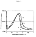
- Implantation profiles of wafers at a dose of 5 x 10 16 /cm 2 (Curve A: implantation at room temperature, Curve B: implantation at -55°C), and implantation profiles of wafers at a dose of 6.5 x 10 16 /cm 2 (Curve C: implantation at room temperature, Curve D: implantation at -55°C) are shown in Fig. 2. It can be seen that profiles having a narrower breadth along the depth direction, i.e., a sharper shape, were obtained by the low temperature implantation for the both doses.
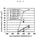
- blister density of each wafer was measured by SEM observation of wafer surface after the wafer was subjected to a heat treatment at a temperature of 400, 450 or 500°C for 30 minutes and shown in Fig. 3.
- the temperature can be lowered to a temperature lower than 500°C, in particular, 450°C or lower.
- a temperature lower than 500°C in particular, 450°C or lower.
- the delamination is caused by the subsequent heat treatment at the dose of 5 x 10 16 /cm 2 , whereas the delamination is unlikely to be caused by the heat treatment at the 'dose of 6.5 x 10 16 /cm 2 .
- the dose required for the delamination can be reduced, and the delamination temperature can also be lowered. Further, it was also found that, when the low temperature implantation is performed, the dose must be suitably controlled according to the wafer temperature, because an excessive dose makes the implanted layer amorphous and thus it becomes difficult to cause the delamination.
- the low temperature implantation improves the implantation profile to narrow the breadth of the implanted hydrogen ions along the depth direction.
- surface roughness of the delaminated plane after the delamination tends to become small. Therefore, the stock removal for the polishing performed for removing the surface roughness of the delaminated plane can be reduced and there can also be obtained an effect that uniformity of film thickness of the SOI layer formed by the ion implantation delamination method is not degraded.
- the ion implantation into the first wafer in the ion implantation delamination method if the ion implantation is performed with maintaining the wafer at a temperature lower than 20°C by forced cooling, while it has conventionally been performed at a temperature of 20°C or higher, the disorder of the lattices in the wafer to be implanted with ions can be reduced and thus the implantation profile can be improved. As a result, the implantation dose required for the delamination can be reduced and breakage of wafer during the bonding heat treatment can be prevented by decrease of the delamination temperature.
- the temperature of the wafer to be implanted with ions is most preferably the absolute zero in order to minimize the disorder of lattices, if it is maintained to be a temperature lower than 20°C, the effect of improving implantation profile can surely be obtained compared with the conventional implantation performed at 20-450°C.
- the temperature is preferably 0°C or lower.
- liquid nitrogen which is relatively inexpensive and easily obtained, can be used to maintain the temperature as low as -196°C.
- a low temperature up to about -269°C can be maintained by using liquid helium and thus the profile can be made close to the theoretical profile. Therefore, the implantation dose can be further reduced, and it is also advantageous for decrease of the delamination temperature.
- the heat treatment temperature in the delamination step can be lowered to a temperature lower than 500°C, in particular, 450°C or lower. Further, if the implantation is performed at an extremely low temperature, it may become possible to attain the delamination at room temperature without performing the delamination heat treatment.
- wafers to be bonded can be arbitrarily selected according to the purpose, and are not particularly limited. However, if a silicon single crystal wafer is used as the first wafer, for example, an SOI wafer having an extremely uniform SOI layer can be produced at a low cost, and it can be widely used for various devices. Moreover, in case of silicon wafers, it is suitable for the production of wafers of larger diameter.
- an oxide film is preferably formed beforehand on the surface of the first wafer before the implantation. This is because, if a thermal oxide film or another oxide film such as CVD oxide film is formed on the surface before the ion implantation, broadening of the implantation profile along the depth direction due to the channeling phenomenon during the ion implantation can be reduced, and thus the implantation profile can be more stabilized. Further, if an oxide film is formed on the first wafer, generation of voids that constitute unbonded portion during the bonding can also be reduced.
- a silicon single crystal wafer can be used, and wafers other than silicon can also be used depending on the purpose.
- a silicon single crystal wafer is used as the second wafer, i.e., a base wafer (support substrate), an extremely flat wafer can be obtained.
- flatness of wafers after bonding is also improved, and it will be preferable also for the subsequent device production step.
- the delamination temperature can be lowered according to the present invention, wafer becomes unlikely to be broken during the delamination heat treatment. Therefore, it is possible to use various wafers having a thermal expansion coefficient different from that of the first wafer as the second wafer.
- a silicon single crystal wafer is used as the first wafer and an insulator wafer consisting essentially of quartz, sapphire, silicon nitride, aluminum nitride or the like is used as the second wafer, there can be obtained an SOI wafer suitable for TFT-LCD.
- the first wafer there was prepared a silicon single crystal wafer having a diameter of 150 mm, plane orientation of (100) and thickness of 625 ⁇ m, on which a silicon oxide film having a thickness of 400 nm was formed on the surface by thermal oxidation.
- This wafer was set on the wafer holder 7 of the ion implantation apparatus shown in Fig. 1 and implanted with hydrogen ions through the oxide film from the wafer surface with the conditions of an implantation energy of 88 keV and a dose of 5 x 10 16 /cm 2 in a state that the wafer was maintained at a low temperature of -55°C by using the thermoregulator 11.
- the wafer after the ion implantation and a silicon single crystal wafer (second wafer) having the same shape as the first wafer, on which an oxide film was not formed on the surface were bonded with each other at room temperature and subjected to a delamination heat treatment at 420°C for 30 minutes under a nitrogen atmosphere.
- the first wafer implanted with ions was successfully delaminated at the ion-implanted layer and an SOI wafer having an SOI layer with a thickness of about 0.4 ⁇ m was produced although the wafers were subjected to a heat treatment at a lower temperature compared with the conventional practice, i.e., 420°C.
- the first wafer there was prepared a silicon single crystal wafer having a diameter of 100 mm, plane orientation of (100) and thickness of 200 ⁇ m, on which a silicon oxide film having a thickness of 400 nm was formed on the surface by thermal oxidation.
- This wafer was set on the wafer holder 7 of the ion implantation apparatus shown in Fig. 1 and implanted with hydrogen ions through the oxide film from the wafer surface with the conditions of an implantation energy of 88 keV and a dose of 5 x 10 16 /cm 2 in a state that the wafer was maintained at a low temperature of -55°C by using the thermoregulator 11.
- the wafer after the ion implantation and a quartz wafer (second wafer) having the same shape as the first wafer were bonded with each other at room temperature and subjected to a heat treatment at 420°C for 30 minutes under a nitrogen atmosphere.
- the wafer implanted with ions was successfully delaminated at the ion-implanted layer without breakage due to the heat treatment, and an SOI wafer having an SOI layer with a thickness of about 0.4 ⁇ m on the quartz wafer could be produced.
Landscapes
- Element Separation (AREA)
- Crystals, And After-Treatments Of Crystals (AREA)
- Physical Vapour Deposition (AREA)
Abstract
In a method for producing a bonded wafer
comprising an ion implantation step where at
least either hydrogen ions or rare gas ions are
implanted into a first wafer from its surface to
form a micro bubble layer (implanted layer) in
the first wafer, a bonding step wherein the
surface subjected to the ion implantation of the
first wafer is bonded to a surface of a second
wafer, and a delamination step where the bonded
first wafer and second wafer are subjected to a
heat treatment to delaminate the first wafer at
the micro bubble layer, wherein the ion
implantation is performed while temperature of
the first' wafer is maintained at a temperature
lower than 20°C in the ion implantation step.
There is provided a method for producing a bonded
wafer, which enables improvement of productivity
and decrease of cost by reduction of implantation
dose required for the delamination and bonding of
wafers without causing breakage of the wafers by
lowering delamination temperature in the ion
implantation delamination method even when wafers
having different thermal expansion coefficients
are bonded.
Description
The present invention relates to the so-called
ion implantation delamination method, in
which a wafer (first wafer, bond wafer) implanted
with hydrogen ions or rare gas ions is bonded to
another wafer (second wafer, base wafer) and then
delaminated by a heat treatment to produce a
bonded wafer, and it relates to a method for
producing a bonded wafer based on the ion
implantation delamination method that can reduce
dose of ions to be implanted and lower
delamination temperature compared with
conventional practice.
As a method for producing an SOI (Silicon On
Insulator) wafer using the bonding method, there
is conventionally known a technique comprising
bonding two of silicon wafers via a silicon oxide
film, for example, a method comprising forming an
oxide film on at least one of such wafers,
bonding the wafers to each other without
interposing foreign matters between the surfaces
to be bonded, and then subjecting them to a heat
treatment at a temperature of 200-1200°C to
enhance the bonding strength, as disclosed in
Japanese Patent Publication (Kokoku) No. 5-46086.
The bonded wafer, of which bonding strength
is enhanced by such a heat treatment, can be
subjected to subsequent grinding and polishing
processes. Therefore, an SOI layer for
fabricating devices can be formed by reducing
thickness of the wafer (first wafer, bond wafer)
on which devices are to be fabricated to a
desired thickness by grinding and polishing.
A bonded SOI wafer produced as described
above has advantages of superior crystallinity of
SOI layer and high reliability of buried oxide
layer existing directly under the SOI layer.
However, because it is produced through reduction
of thickness of the first wafer by grinding and
polishing, it suffers from a drawback that the
reduction of thickness takes a lot of time and
generates waste of the material. In addition,
obtainable uniformity of the thickness of the SOI
layer is only in such a degree of target
thickness ± 0.3 µm or so at most.
Meanwhile, in connection with recent use of
higher integration degree and higher processing
velocity of semiconductor devices, further
reduction of film thickness and improvement of
film thickness uniformity are required as for the
thickness of the SOI layer. Specifically, a film
thickness and uniformity represented as 0.1 ±
0.01 µm or so are required.
A thin film SOI wafer having such a film
thickness and film thickness uniformity cannot be
realized as a bonded wafer by the conventional
thickness reduction processing using only
grinding and polishing. Therefore, the method
called ion implantation delamination method or
hydrogen ion delamination method was developed as
a novel film thickness reduction technique as
disclosed in Japanese Patent Laid-open (Kokai)
Publication No. 5-211128.
This ion implantation delamination method is
a technique for producing an SOI wafer, wherein
an oxide film is formed on at least one of two
silicon wafers, for example, hydrogen ions or
rare gas ions are implanted into one wafer from
its top surface to form a micro bubble layer
(enclosed layer) in the silicon wafer, then the
ion-implanted surface of the wafer is bonded to
the other wafer via the oxide film, thereafter
one of the wafers is delaminated as a thin film
at the micro bubble layer as a cleavage plane
(delaminating plane) by a heat treatment
(delamination heat treatment), and the other
bonded wafer is further subjected to a heat
treatment (bonding heat treatment) to strengthen
the bonding to obtain an SOI wafer.
In this method, the delaminated plane is
obtained as a good mirror surface, and an SOI
wafer having extremely high uniformity of the
thickness of SOI layer can be obtained relatively
easily. In addition, the method also has an
advantage that one delaminated wafer can be
reused and thus the material can be used
effectively.
Further, by this method, it is also possible
to directly bond silicon wafers to each other
without an oxide film, and it can be used not
only for a case where silicon wafers are bonded
to each other, but also for a case where an ion-implanted
silicon wafer is bonded to an insulator
wafer having a different thermal expansion
coefficient such as those of quartz, sapphire,
silicon nitride, aluminum nitride and so forth or
an ion-implanted insulator wafer is bonded to
another wafer to obtain a wafer having a thin
film of such materials and so forth.
Although this ion implantation delamination
method is an extremely excellent method as a
method for producing a bonded SOI wafer, it has
the following problems for practical use.
One of the problems is higher production
cost, because the implantation dose (dose) must
be increased to some extent in order to cause the
delamination. That is, an implantation dose
exceeding 1 x 10¹⁶/cm2 (for example, 5 x 10¹⁶/cm2)
is required as the implantation dose for causing
delamination as disclosed in Japanese Patent
Laid-open (Kokai) Publication No. 5-211128.
Therefore, the implantation time is prolonged,
and increase of cost is invited due to reduction
of throughput. Thus, it is desired to reduce the
implantation dose.
Further, Japanese Patent Laid-open
Publication No. 5-211158 describes that a
temperature exceeding about 500°C is required for
a heat treatment for causing delamination at an
ion-implanted layer in a silicon wafer implanted
with ions at a dose of the above-specified level
and bonded to another wafer. However, there
exists a problem that, in a case where a silicon
wafer is bonded with a wafer having a thermal
expansion coefficient different from that of
silicon such as an insulator wafer, if the bonded
wafers are subjected to a heat treatment at a
temperature exceeding about 500°C, one of the
wafers may be broken during heating or cooling.
To solve this problem, the applicants of the
present application proposed a method of
repeating heat treatment and reduction of film
thickness and a method of implanting deuterium
ions in the previous applications (Japanese
Patent Laid-open Publication Nos. 11-145438 and
11-330438). However, neither of these methods
can be necessarily considered a simple method.
Furthermore, although the ion implantation
delamination method provides an SOI wafer having
extremely high uniformity of SOI layer thickness
as described above and a mirror surface as the
delaminated plane, the delaminated plane suffers
from measurable surface roughness and crystal
defects are generated by the ion implantation.
Therefore, to eliminate these, it is necessary to
polish the surface of SOI layer, although it may
be done for a small amount. Although this
polishing is mirror polishing using an extremely
small stock removal for polishing (5 nm to 400
nm) called touch polish, it suffers from a
problem that it may degrade thickness uniformity
improved by the ion implantation delamination
method with much trouble with increase of the
stock removal for polishing.
The present invention was accomplished in
view of the aforementioned problems, and its
object is to provide a method for producing a
bonded wafer, which enables improvement of
productivity and decrease of cost by reduction of
implantation dose required for the delamination
and bonding of wafers without causing breakage of
the wafers by lowering delamination temperature
in the ion implantation delamination method even
when wafers having different thermal expansion
coefficients are bonded.
In order to achieve the aforementioned
object, the method for producing a bonded wafer
according to the present invention is a method
for producing a bonded wafer comprising an ion
implantation step where at least either hydrogen
ions or rare gas ions are implanted into a first
wafer from its surface to form a micro bubble
layer (implanted layer) in the first wafer, a
bonding step wherein the surface subjected to the
ion implantation of the first wafer is bonded to
a surface of a second wafer, and a delamination
step where the bonded first wafer and second
wafer are subjected to a heat treatment to
delaminate the first wafer at the micro bubble
layer, wherein the ion implantation is performed
while temperature of the first wafer is
maintained at a temperature lower than 20°C in
the ion implantation step.
If the ion implantation is performed while
maintaining the temperature of the first wafer at
a temperature lower than 20°C, disorder of
lattices in the wafer implanted with ions can be
made small, and thus the implantation profile can
be improved. As a result, the implantation dose
required for the delamination can be reduced and
breakage of wafers during the bonding heat
treatment can be prevented by use of a lower
delamination temperature.
In this case, the temperature of the first
wafer is more preferably maintained at 0°C or
lower during the aforementioned ion implantation
step.
In order to enhance the improvement effect
of the implantation profile, it is preferable to
control the temperature of the first wafer to be
0°C or lower as described above. In particular,
if liquid nitrogen, which it is relatively
inexpensive and easily obtained, is used in order
to maintain the temperature of the first wafer to
be a temperature of 0°C or lower, it is possible
to maintain the wafer at a low temperature as low
as -196°C, and if liquid helium is used, it is
possible to maintain the wafer at a low
temperature as low as about -269°C. Thus, the
profile can be made closer to the theoretical
profile, and therefore the implantation dose can
be further reduced and it is also advantageous
for lowering the delamination temperature.
In the present invention, the heat treatment
temperature during the aforementioned
delamination step can be lower than 500°C.
According to the present invention, the
implantation profile is improved, and therefore
it becomes possible to cause the delamination at
a temperature lower than 500°C as described above.
Therefore, even when wafers having different
thermal expansion coefficients are bonded, they
can be bonded without generating breakage of the
wafers.
Further, in the present invention, a silicon
single crystal wafer can be used as the first
wafer.
If a silicon single crystal wafer is used as
the first wafer as described above, an SOI wafer
that has very uniform SOI layer thickness can be
produced at a low cost, and therefore it can be
widely used for various devices.
Further, it is also preferable to
preliminarily form an oxide film on the surface
of the first wafer before the ion implantation.
This is because, if a thermal oxide film, a
CVD oxide film or the like is formed on the
surface before the ion implantation, degradation
of the implantation profile (broadening along the
depth direction) due to the channeling phenomenon
during the ion implantation can be reduced, and
generation of voids (unbonded portion) during the
bonding with the second wafer can also be reduced.
Further, in the present invention, as the
second wafer, a silicon single crystal wafer can
be used, and a wafer having a thermal expansion
coefficient different from that of the first
wafer can also be used.
If a silicon single crystal wafer is used as
the second wafer, i.e., the base wafer, a wafer
excellent in flatness can be obtained, and
moreover, a wafer having a large diameter of 200
mm or 300 mm or larger can also be obtained.
On the other hand, since the delamination
temperature can be lowered according to the
present invention, it becomes possible to produce
a bonded wafer without causing breakage of wafers
even when a wafer having a thermal expansion
coefficient different from that of the first
wafer is bonded. Therefore, for example, even if
a silicon single crystal wafer is used as the
first wafer and an insulator wafer consisting
essentially of quartz, sapphire, silicon nitride,
aluminum nitride or the like, which has a thermal
expansion coefficient different from silicon, is
used as the second wafer, they can be easily
bonded without causing breakage.
Furthermore, an oxide film may be
preliminarily formed on a surface of the second
wafer before bonding.
By forming a thermal oxide film, a CVD oxide
film or the like on the second wafer surface as
described above, the generation of voids due to
the bonding with the first wafer can be reduced.
Further, a bonded wafer of extremely high
quality can be obtained by the method of the
present invention.
In the present invention, in particular, an
SOI wafer that has an SOI layer of extremely high
thickness uniformity can be obtained, and there
can be provided not only a bonded wafer
consisting of bonded silicon wafers, but also a
bonded wafer consisting of a silicon wafer bonded
with an insulator wafer and a bonded wafer
consisting of bonded insulator wafers.
As described above, according to the present
invention, the implantation profile can be
improved to obtain a sharp distribution in the
ion implantation delamination method by forcibly
cooling the wafer during the ion implantation to
maintain it at a low temperature. As a result,
the implantation dose required for the
delamination can be reduced, thus productivity is
improved and it becomes possible to reduce the
cost.
Further, since the implantation profile is
improved and the implantation damage layer in the
wafer becomes thin, the surface roughness of the
delaminated plane becomes small. As a result,
the stock removal for polishing performed for the
delaminated plane can be reduced, and therefore
there can also be obtained an advantage that the
degradation of precision for thin film layer
thickness caused by polishing can be suppressed
to the minimum extent.
Furthermore, since it also becomes possible
to lower the delamination temperature, a bonded
wafer of high quality can be produced without
causing breakage of wafers and also without
performing troublesome steps such as repetition
of heat treatment, even when wafers having
different thermal expansion coefficients are
bonded.
Hereafter, embodiments of the present
invention will be explained in detail. However,
the present invention is not limited to these.
In order to reduce the implantation dose
required for the delamination and lower the
delamination temperature in the ion implantation
delamination method, the inventors of the present
invention directed their attention to the
temperature of the wafer during the ion
implantation.
That is, in the conventional ion
implantation delamination method, the temperature
of the wafer subjected to the ion implantation is
maintained at a temperature lower than the
critical temperature at which the gas generated
by implanted ions begins to be rapidly diffused
and emitted from semiconductors, and in the case
of silicon, it was presupposed that a
implantation temperature of 20-450°C should be
preferred, as disclosed in Japanese Patent Laid-open
Publication No. 5-211128. Therefore, the
hydrogen ion implantation is usually performed at
room temperature in many cases. However, since
the ions are implanted with high energy although
the ion implantation is performed at room
temperature, it is presumed that the temperature
of the wafer reaches 60 to 70°C. Therefore, it
is considered that the implanted hydrogen ions
are diffused through the disordered lattices to
some extent by heat, and they have a distribution
more spreading along the depth direction of the
wafer compared with the theoretically obtained
implantation profile of the ion implanted layer.
Therefore, the inventors of the present
invention conceived that, if a wafer was
maintained at a temperature as low as possible by
forcibly cooling the wafer during the ion
implantation, the implantation profile would be
improved and thus a sharp distribution near the
theoretical profile based on the assumption of
the absolute zero could be expected, and thus
accomplished the present invention.
That is, the following experiments were
performed in order to confirm the effect of the
aforementioned ion implantation at a low
temperature.
First, a silicon single crystal wafer of
plane orientation (100) was prepared, on which a
silicon oxide film having a thickness 400 nm was
formed by thermal oxidation on the surface.
Hydrogen ions were implanted through the surface
oxide film of this wafer under the following
conditions.
The outline of the used apparatus was
similar to that of a usual ion implantation
apparatus as shown in Fig. 1A. However, it had a
part for holding a wafer that can be cooled with
a refrigerant such as liquid nitrogen and liquid
helium, whereas it is usually cooled only with
cooling water, and provided with temperature
controlling function so that the temperature of
the wafer can be controlled as shown in Fig. 1B.
That is, as shown in Fig. 1A, the ion
implantation apparatus comprises an ion source 1
that ionizes a raw material of ions, electrodes 2
withdrawing such ions, a mass spectrometer 3 that
separates various types of the withdrawn ions, an
accelerator 4 that accelerates the ions with high
voltage, and multiple deflection plates 5 for
uniformly irradiating the wafer W held on a
holding part 6 with ion beams.
As shown in Fig. 1B, in the part 6 for
holding the wafer W, refrigerant tanks 9 are
connected to a wafer holder 7 for holding the
wafer W via a control valve 8, so that the wafer
W can be cooled by using a desired refrigerant
that is selected depending on the temperature at
which the wafer W should be maintained. The
temperature of the wafer holder 7 is measured by
a thermometer 10, and data obtained by it are
sent to a thermoregulator 11. The
thermoregulator 11 controls flow rate and
temperature of the refrigerant by controlling
opening degree of the control valve 8 and so
forth so that the wafer W can be maintained at a
predetermined temperature.
A wafer implanted with hydrogen ions was
evaluated by the following three kinds of methods.
Implantation profiles of wafers at a dose of
5 x 10¹⁶/cm2 (Curve A: implantation at room
temperature, Curve B: implantation at -55°C), and
implantation profiles of wafers at a dose of 6.5
x 1016/cm2 (Curve C: implantation at room
temperature, Curve D: implantation at -55°C) are
shown in Fig. 2. It can be seen that profiles
having a narrower breadth along the depth
direction, i.e., a sharper shape, were obtained
by the low temperature implantation for the both
doses.
Since density of blisters after heat
treatment directly relates to delamination,
blister density of each wafer was measured by SEM
observation of wafer surface after the wafer was
subjected to a heat treatment at a temperature of
400, 450 or 500°C for 30 minutes and shown in Fig.
3.
From the results shown in Fig. 3, it was
found that blisters were generated at extremely
higher densities in the wafer for which the
implantation was performed at -55°C at a dose of
5 x 10¹⁶/cm2 (plotted with white circles) and the
wafers for which the implantation was performed
at -20°C at a dose of 5 x 10¹⁶/cm2 or 6.5 x
1016/cm2 (plotted with white squares and black
squares) compared with the wafers for which the
implantation was performed at room temperature at
the same doses (plotted with white triangles and
black triangles). Therefore, it can be seen that
the low temperature implantation can lower the
heat treatment temperature required for the
delamination compared with the room temperature
implantation. For example, it can be seen that
the temperature can be lowered to a temperature
lower than 500°C, in particular, 450°C or lower.
The reason why blisters could not be obtained at
a high density in the wafer for which the
implantation was performed at -55°C at a dose of
6.5 x 10¹⁶/cm2 (plotted with black circles) will
be described later.
As for the wafer for which the implantation
was performed at -55°C, a portion of wafer cross
section near the implanted layer was observed by
TEM before and after a heat treatment at 400°C.
When the dose was 5 x 10¹⁶/cm2, defects (micro
bubbles) required for the delamination were
observed at the implanted layer before the heat
treatment, and cracks consisting of aggregated
blisters were observed near the center part of
the implanted layer after the heat treatment. On
the other hand, when the dose was 6.5 x 10¹⁶/cm2,
defects required for the delamination were not
observed at the implanted layer before the heat
treatment and crystals of the portion
corresponding to the implanted layer became
amorphous. Further, after the heat treatment,
blisters near the center part of the implanted
layer, which were observed at the dose of 5 x
1016/cm2, were not observed and only a few
blisters were observed at the boundary of the
amorphous layer and the deeper crystal layer.
These indicate that, as for the low
temperature implantation (-55°C in this case),
the delamination is caused by the subsequent heat
treatment at the dose of 5 x 10¹⁶/cm2, whereas the
delamination is unlikely to be caused by the heat
treatment at the 'dose of 6.5 x 10¹⁶/cm2. This was
considered to be caused because the distribution
of hydrogen was improved by the low temperature
implantation compared with the room temperature
implantation so that defects for the delamination
were effectively formed, and as a result, the
dose of 6.5 x 10¹⁶/cm2 became excessive so that
the crystals became amorphous, not forming
defects, and generation of blisters became
difficult.
From the above results, it was found that,
by performing the low temperature implantation,
the dose required for the delamination can be
reduced, and the delamination temperature can
also be lowered. Further, it was also found that,
when the low temperature implantation is
performed, the dose must be suitably controlled
according to the wafer temperature, because an
excessive dose makes the implanted layer
amorphous and thus it becomes difficult to cause
the delamination.
Furthermore, as described above, the low
temperature implantation improves the
implantation profile to narrow the breadth of the
implanted hydrogen ions along the depth direction.
Thus, surface roughness of the delaminated plane
after the delamination tends to become small.
Therefore, the stock removal for the polishing
performed for removing the surface roughness of
the delaminated plane can be reduced and there
can also be obtained an effect that uniformity of
film thickness of the SOI layer formed by the ion
implantation delamination method is not degraded.
Thus, in the ion implantation into the first
wafer in the ion implantation delamination method,
if the ion implantation is performed with
maintaining the wafer at a temperature lower than
20°C by forced cooling, while it has
conventionally been performed at a temperature of
20°C or higher, the disorder of the lattices in
the wafer to be implanted with ions can be
reduced and thus the implantation profile can be
improved. As a result, the implantation dose
required for the delamination can be reduced and
breakage of wafer during the bonding heat
treatment can be prevented by decrease of the
delamination temperature.
While the temperature of the wafer to be
implanted with ions is most preferably the
absolute zero in order to minimize the disorder
of lattices, if it is maintained to be a
temperature lower than 20°C, the effect of
improving implantation profile can surely be
obtained compared with the conventional
implantation performed at 20-450°C.
In particular, in order to enhance the
effect of improving implantation profile, the
temperature is preferably 0°C or lower. To
maintain such a temperature, liquid nitrogen,
which is relatively inexpensive and easily
obtained, can be used to maintain the temperature
as low as -196°C. Further, a low temperature up
to about -269°C can be maintained by using liquid
helium and thus the profile can be made close to
the theoretical profile. Therefore, the
implantation dose can be further reduced, and it
is also advantageous for decrease of the
delamination temperature.
Moreover, since the implantation profile is
improved by the low temperature ion implantation,
the heat treatment temperature in the
delamination step can be lowered to a temperature
lower than 500°C, in particular, 450°C or lower.
Further, if the implantation is performed at an
extremely low temperature, it may become possible
to attain the delamination at room temperature
without performing the delamination heat
treatment.
As described above, while the delamination
heat treatment must have conventionally been
performed at a temperature of 500°C or higher, it
becomes possible to attain the delamination at a
temperature lower than 500°C. Therefore,
breakage of wafers is not caused as in the
conventional techniques even when wafers having
different thermal expansion coefficients are
bonded as in the case of bonding of a silicon
wafer and an insulator wafer, and there is also
obtained an advantage that it is not required to
perform a troublesome operation such as
repetition of heat treatment and film thickness
reduction.
In the present invention, wafers to be
bonded can be arbitrarily selected according to
the purpose, and are not particularly limited.
However, if a silicon single crystal wafer is
used as the first wafer, for example, an SOI
wafer having an extremely uniform SOI layer can
be produced at a low cost, and it can be widely
used for various devices. Moreover, in case of
silicon wafers, it is suitable for the production
of wafers of larger diameter.
Further, an oxide film is preferably formed
beforehand on the surface of the first wafer
before the implantation. This is because, if a
thermal oxide film or another oxide film such as
CVD oxide film is formed on the surface before
the ion implantation, broadening of the
implantation profile along the depth direction
due to the channeling phenomenon during the ion
implantation can be reduced, and thus the
implantation profile can be more stabilized.
Further, if an oxide film is formed on the first
wafer, generation of voids that constitute
unbonded portion during the bonding can also be
reduced.
As the second wafer, a silicon single
crystal wafer can be used, and wafers other than
silicon can also be used depending on the purpose.
If a silicon single crystal wafer is used as
the second wafer, i.e., a base wafer (support
substrate), an extremely flat wafer can be
obtained. Thus, flatness of wafers after bonding
is also improved, and it will be preferable also
for the subsequent device production step. In
addition, it is also relatively easy to obtain
wafers having a large diameter of 200 mm or 300
mm or larger.
Furthermore, since the delamination
temperature can be lowered according to the
present invention, wafer becomes unlikely to be
broken during the delamination heat treatment.
Therefore, it is possible to use various wafers
having a thermal expansion coefficient different
from that of the first wafer as the second wafer.
In this case, if a silicon single crystal wafer
is used as the first wafer and an insulator wafer
consisting essentially of quartz, sapphire,
silicon nitride, aluminum nitride or the like is
used as the second wafer, there can be obtained
an SOI wafer suitable for TFT-LCD.
Furthermore, it is also preferable to
preliminarily form an oxide film also on the
surface of the second wafer, and then used for
the bonding. By doing so, generation of voids
can be prevented during the bonding with the
first wafer.
Hereafter, the present invention will be
specifically explained with reference to the
following examples of the present invention and
comparative example. However, the present
invention is not limited by these.
As the first wafer, there was prepared a
silicon single crystal wafer having a diameter of
150 mm, plane orientation of (100) and thickness
of 625 µm, on which a silicon oxide film having a
thickness of 400 nm was formed on the surface by
thermal oxidation. This wafer was set on the
wafer holder 7 of the ion implantation apparatus
shown in Fig. 1 and implanted with hydrogen ions
through the oxide film from the wafer surface
with the conditions of an implantation energy of
88 keV and a dose of 5 x 10¹⁶/cm2 in a state that
the wafer was maintained at a low temperature of
-55°C by using the thermoregulator 11.
Subsequently, the wafer after the ion
implantation and a silicon single crystal wafer
(second wafer) having the same shape as the first
wafer, on which an oxide film was not formed on
the surface, were bonded with each other at room
temperature and subjected to a delamination heat
treatment at 420°C for 30 minutes under a
nitrogen atmosphere.
As a result, the first wafer implanted with
ions was successfully delaminated at the ion-implanted
layer and an SOI wafer having an SOI
layer with a thickness of about 0.4 µm was
produced although the wafers were subjected to a
heat treatment at a lower temperature compared
with the conventional practice, i.e., 420°C.
Wafers produced with the same conditions as
those of Example 1 except that the wafer
temperature during the ion implantation was 25°C
and bonded with each other at room temperature
were subjected to a heat treatment at 420°C for
30 minutes under a nitrogen atmosphere as in
Example 1.
As a result, delamination was not generated
at the ion-implanted layer, but in order to
delaminate the first wafer, it was required to
perform a heat treatment at a higher temperature
or further increase the ion implantation dose.
As the first wafer, there was prepared a
silicon single crystal wafer having a diameter of
100 mm, plane orientation of (100) and thickness
of 200 µm, on which a silicon oxide film having a
thickness of 400 nm was formed on the surface by
thermal oxidation. This wafer was set on the
wafer holder 7 of the ion implantation apparatus
shown in Fig. 1 and implanted with hydrogen ions
through the oxide film from the wafer surface
with the conditions of an implantation energy of
88 keV and a dose of 5 x 10¹⁶/cm2 in a state that
the wafer was maintained at a low temperature of
-55°C by using the thermoregulator 11.
Subsequently, the wafer after the ion
implantation and a quartz wafer (second wafer)
having the same shape as the first wafer were
bonded with each other at room temperature and
subjected to a heat treatment at 420°C for 30
minutes under a nitrogen atmosphere.
As a result, the wafer implanted with ions
was successfully delaminated at the ion-implanted
layer without breakage due to the heat treatment,
and an SOI wafer having an SOI layer with a
thickness of about 0.4 µm on the quartz wafer
could be produced.
The present invention is not limited to the
embodiments described above. The above-described
embodiments are mere examples, and those having
the substantially same technical characteristics
as those described in the appended claims and
providing similar functions and advantages are
all included in the scope of the present
invention.
Claims (9)
- A method for producing a bonded wafer comprising an ion implantation step where at least either hydrogen ions or rare gas ions are implanted into a first wafer from its surface to form a micro bubble layer (implanted layer) in the first wafer, a bonding step wherein the surface subjected to the ion implantation of the first wafer is bonded to a surface of a second wafer, and a delamination step where the bonded first wafer and second wafer are subjected to a heat treatment to delaminate the first wafer at the micro bubble layer, wherein the ion implantation is performed while temperature of the first wafer is maintained at a temperature lower than 20°C in the ion implantation step.
- The method for producing a bonded wafer according to Claim 1, wherein the temperature of the first wafer is maintained at 0°C or lower during the ion implantation step.
- The method for producing a bonded wafer according to Claim 1 or 2, wherein the heat treatment temperature during the delamination step is lower than 500°C.
- The method for producing a bonded wafer according to any one of Claims 1-3, wherein a silicon single crystal wafer is used as the first wafer.
- The method for producing a bonded wafer according to any one of Claims 1-4, wherein an oxide film is preliminarily formed on the surface of the first wafer before the ion implantation.
- The method for producing a bonded wafer according to any one of Claims 1-5, wherein a silicon single crystal wafer is used as the second wafer.
- The method for producing a bonded wafer according to any one of Claims 1-6, wherein a wafer having a thermal expansion coefficient different from that of the first wafer is used as the second wafer.
- The method for producing a bonded wafer according to any one of Claims 1-7, wherein an oxide film is preliminarily formed on a surface of the second wafer before bonding.
- A bonded wafer, which is produced by the method according to any one of Claims 1-8.
Applications Claiming Priority (3)
| Application Number | Priority Date | Filing Date | Title |
|---|---|---|---|
| JP2000086255A JP2001274368A (en) | 2000-03-27 | 2000-03-27 | Method of manufacturing bonded wafer and bonded wafer manufactured by this method |
| JP2000086255 | 2000-03-27 | ||
| PCT/JP2001/002235 WO2001073848A1 (en) | 2000-03-27 | 2001-03-21 | Production method for bonding wafer and bonding wafer produced by this method |
Publications (2)
| Publication Number | Publication Date |
|---|---|
| EP1189285A1 true EP1189285A1 (en) | 2002-03-20 |
| EP1189285A4 EP1189285A4 (en) | 2008-04-02 |
Family
ID=18602453
Family Applications (1)
| Application Number | Title | Priority Date | Filing Date |
|---|---|---|---|
| EP01914187A Withdrawn EP1189285A4 (en) | 2000-03-27 | 2001-03-21 | PROCESS FOR PRODUCING LINK PADS AND LINK PADS PRODUCED THEREBY |
Country Status (6)
| Country | Link |
|---|---|
| US (1) | US20020157790A1 (en) |
| EP (1) | EP1189285A4 (en) |
| JP (1) | JP2001274368A (en) |
| KR (1) | KR100776381B1 (en) |
| TW (1) | TW487974B (en) |
| WO (1) | WO2001073848A1 (en) |
Cited By (5)
| Publication number | Priority date | Publication date | Assignee | Title |
|---|---|---|---|---|
| FR2856192A1 (en) * | 2003-06-11 | 2004-12-17 | Soitec Silicon On Insulator | PROCESS FOR PRODUCING HETEROGENEOUS STRUCTURE AND STRUCTURE OBTAINED BY SUCH A METHOD |
| EP1936679A1 (en) * | 2006-12-18 | 2008-06-25 | Shinetsu Chemical Co., Ltd. | Method for manufacturing an SOI substrate |
| WO2008036529A3 (en) * | 2006-09-23 | 2008-08-28 | Varian Semiconductor Equipment | Techniques for temperature-controlled ion implantation |
| WO2008067213A3 (en) * | 2006-11-27 | 2008-09-12 | Varian Semiconductor Equipment | Techniques for low temperature ion implantation |
| WO2009118374A1 (en) * | 2008-03-28 | 2009-10-01 | S.O.I.Tec Silicon On Insulator Technologies | Controlled temperature implantation |
Families Citing this family (22)
| Publication number | Priority date | Publication date | Assignee | Title |
|---|---|---|---|---|
| JP2002015971A (en) * | 2000-06-27 | 2002-01-18 | Matsushita Electric Ind Co Ltd | Pattern forming method and semiconductor device manufacturing apparatus |
| KR100483956B1 (en) * | 2002-08-10 | 2005-04-18 | 한국과학기술원 | Method of minimizing thermal stress in reversible wafer bonding technique of compound semiconductor wafer |
| FR2847077B1 (en) * | 2002-11-12 | 2006-02-17 | Soitec Silicon On Insulator | SEMICONDUCTOR COMPONENTS, PARTICULARLY OF THE MIXED SOI TYPE, AND METHOD OF MAKING SAME |
| US20040187769A1 (en) * | 2003-03-27 | 2004-09-30 | Yoshirou Aoki | Method of producing SOI wafer |
| EP1652230A2 (en) * | 2003-07-29 | 2006-05-03 | S.O.I.Tec Silicon on Insulator Technologies | Method for obtaining a thin high-quality layer by co-implantation and thermal annealing |
| FR2864336B1 (en) * | 2003-12-23 | 2006-04-28 | Commissariat Energie Atomique | METHOD FOR SEALING TWO PLATES WITH FORMATION OF AN OHMIC CONTACT BETWEEN THEM |
| US7939424B2 (en) * | 2007-09-21 | 2011-05-10 | Varian Semiconductor Equipment Associates, Inc. | Wafer bonding activated by ion implantation |
| JP5522917B2 (en) | 2007-10-10 | 2014-06-18 | 株式会社半導体エネルギー研究所 | Manufacturing method of SOI substrate |
| US8329260B2 (en) * | 2008-03-11 | 2012-12-11 | Varian Semiconductor Equipment Associates, Inc. | Cooled cleaving implant |
| JP5263509B2 (en) * | 2008-09-19 | 2013-08-14 | 信越半導体株式会社 | Manufacturing method of bonded wafer |
| SG160300A1 (en) * | 2008-10-03 | 2010-04-29 | Semiconductor Energy Lab | Method for manufacturing soi substrate |
| SG176602A1 (en) * | 2009-06-24 | 2012-01-30 | Semiconductor Energy Lab | Method for reprocessing semiconductor substrate and method for manufacturing soi substrate |
| US8278187B2 (en) * | 2009-06-24 | 2012-10-02 | Semiconductor Energy Laboratory Co., Ltd. | Method for reprocessing semiconductor substrate by stepwise etching with at least two etching treatments |
| SG178061A1 (en) * | 2009-08-25 | 2012-03-29 | Semiconductor Energy Lab | Method for reprocessing semiconductor substrate, method for manufacturing reprocessed semiconductor substrate, and method for manufacturing soi substrate |
| US8318588B2 (en) * | 2009-08-25 | 2012-11-27 | Semiconductor Energy Laboratory Co., Ltd. | Method for reprocessing semiconductor substrate, method for manufacturing reprocessed semiconductor substrate, and method for manufacturing SOI substrate |
| WO2011043178A1 (en) * | 2009-10-09 | 2011-04-14 | Semiconductor Energy Laboratory Co., Ltd. | Reprocessing method of semiconductor substrate, manufacturing method of reprocessed semiconductor substrate, and manufacturing method of soi substrate |
| JP5644096B2 (en) | 2009-11-30 | 2014-12-24 | ソニー株式会社 | Method for manufacturing bonded substrate and method for manufacturing solid-state imaging device |
| US8748288B2 (en) * | 2010-02-05 | 2014-06-10 | International Business Machines Corporation | Bonded structure with enhanced adhesion strength |
| EP2654074B1 (en) * | 2010-03-31 | 2016-10-26 | EV Group E. Thallner GmbH | Method for permanently connecting two metal surfaces |
| US9123529B2 (en) | 2011-06-21 | 2015-09-01 | Semiconductor Energy Laboratory Co., Ltd. | Method for reprocessing semiconductor substrate, method for manufacturing reprocessed semiconductor substrate, and method for manufacturing SOI substrate |
| JP5670303B2 (en) * | 2011-12-08 | 2015-02-18 | 信越半導体株式会社 | Deterioration judgment method for substrate holder of ion implanter |
| CN109671612B (en) * | 2018-11-15 | 2020-07-03 | 中国科学院上海微系统与信息技术研究所 | A kind of gallium oxide semiconductor structure and preparation method thereof |
Family Cites Families (8)
| Publication number | Priority date | Publication date | Assignee | Title |
|---|---|---|---|---|
| US5244820A (en) * | 1990-03-09 | 1993-09-14 | Tadashi Kamata | Semiconductor integrated circuit device, method for producing the same, and ion implanter for use in the method |
| FR2681472B1 (en) * | 1991-09-18 | 1993-10-29 | Commissariat Energie Atomique | PROCESS FOR PRODUCING THIN FILMS OF SEMICONDUCTOR MATERIAL. |
| JPH09162136A (en) * | 1995-12-13 | 1997-06-20 | Hitachi Ltd | Method for manufacturing semiconductor device |
| JPH101999A (en) * | 1996-06-17 | 1998-01-06 | Kyowa Plast Sangyo Kk | Coupling flange for toilet stool and connecting structure of the flange and toilet stool |
| JP3412449B2 (en) * | 1997-05-29 | 2003-06-03 | 三菱住友シリコン株式会社 | Method for manufacturing SOI substrate |
| US5877070A (en) * | 1997-05-31 | 1999-03-02 | Max-Planck Society | Method for the transfer of thin layers of monocrystalline material to a desirable substrate |
| JP2998724B2 (en) * | 1997-11-10 | 2000-01-11 | 日本電気株式会社 | Manufacturing method of bonded SOI substrate |
| JP3697106B2 (en) * | 1998-05-15 | 2005-09-21 | キヤノン株式会社 | Method for manufacturing semiconductor substrate and method for manufacturing semiconductor thin film |
-
2000
- 2000-03-27 JP JP2000086255A patent/JP2001274368A/en active Pending
-
2001
- 2001-03-21 EP EP01914187A patent/EP1189285A4/en not_active Withdrawn
- 2001-03-21 KR KR1020017015151A patent/KR100776381B1/en not_active Expired - Fee Related
- 2001-03-21 US US09/979,105 patent/US20020157790A1/en not_active Abandoned
- 2001-03-21 WO PCT/JP2001/002235 patent/WO2001073848A1/en not_active Ceased
- 2001-03-26 TW TW090107099A patent/TW487974B/en not_active IP Right Cessation
Cited By (11)
| Publication number | Priority date | Publication date | Assignee | Title |
|---|---|---|---|---|
| FR2856192A1 (en) * | 2003-06-11 | 2004-12-17 | Soitec Silicon On Insulator | PROCESS FOR PRODUCING HETEROGENEOUS STRUCTURE AND STRUCTURE OBTAINED BY SUCH A METHOD |
| US6858517B2 (en) | 2003-06-11 | 2005-02-22 | S.O.I. Tec Silicon On Insulator Technologies S.A. | Methods of producing a heterogeneous semiconductor structure |
| EP1487012A3 (en) * | 2003-06-11 | 2005-11-16 | S.O.I.Tec Silicon on Insulator Technologies | Method of making an heterogeneous structure and structure obtained by said method |
| WO2008036529A3 (en) * | 2006-09-23 | 2008-08-28 | Varian Semiconductor Equipment | Techniques for temperature-controlled ion implantation |
| US7993698B2 (en) | 2006-09-23 | 2011-08-09 | Varian Semiconductor Equipment Associates, Inc. | Techniques for temperature controlled ion implantation |
| WO2008067213A3 (en) * | 2006-11-27 | 2008-09-12 | Varian Semiconductor Equipment | Techniques for low temperature ion implantation |
| US7528392B2 (en) | 2006-11-27 | 2009-05-05 | Varian Semiconductor Equipment Associates, Inc. | Techniques for low-temperature ion implantation |
| EP1936679A1 (en) * | 2006-12-18 | 2008-06-25 | Shinetsu Chemical Co., Ltd. | Method for manufacturing an SOI substrate |
| WO2009118374A1 (en) * | 2008-03-28 | 2009-10-01 | S.O.I.Tec Silicon On Insulator Technologies | Controlled temperature implantation |
| FR2929446A1 (en) * | 2008-03-28 | 2009-10-02 | Soitec Silicon On Insulator | IMPLANTATION AT CONTROLLED TEMPERATURE |
| US8247309B2 (en) | 2008-03-28 | 2012-08-21 | Soitec | Controlled temperature implantation |
Also Published As
| Publication number | Publication date |
|---|---|
| KR20020020895A (en) | 2002-03-16 |
| WO2001073848A1 (en) | 2001-10-04 |
| EP1189285A4 (en) | 2008-04-02 |
| KR100776381B1 (en) | 2007-11-16 |
| TW487974B (en) | 2002-05-21 |
| US20020157790A1 (en) | 2002-10-31 |
| JP2001274368A (en) | 2001-10-05 |
Similar Documents
| Publication | Publication Date | Title |
|---|---|---|
| US20020157790A1 (en) | Method for producing a bonded wafer using ion implantation delamination | |
| US6054363A (en) | Method of manufacturing semiconductor article | |
| JP5363977B2 (en) | Semiconductor-on-insulator structure fabricated using irradiation annealing | |
| EP0843345B1 (en) | Method of manufacturing a semiconductor article | |
| CA2233096C (en) | Substrate and production method thereof | |
| AU728331B2 (en) | Semiconductor substrate and method of manufacturing the same | |
| KR100402155B1 (en) | Process for manufacturing a semiconductor substrate as well as a semiconductor thin film, and multilayer structure | |
| US6429095B1 (en) | Semiconductor article and method of manufacturing the same | |
| US7052948B2 (en) | Film or layer made of semi-conductive material and method for producing said film or layer | |
| US6461939B1 (en) | SOI wafers and methods for producing SOI wafer | |
| EP0843346B1 (en) | Method of manufacturing a semiconductor article | |
| US6900113B2 (en) | Method for producing bonded wafer and bonded wafer | |
| KR101482792B1 (en) | Method for manufacturing soi wafer | |
| US6613676B1 (en) | Process of reclamation of SOI substrate and reproduced substrate | |
| EP2023375A1 (en) | Bonded wafer manufacturing method |
Legal Events
| Date | Code | Title | Description |
|---|---|---|---|
| PUAI | Public reference made under article 153(3) epc to a published international application that has entered the european phase |
Free format text: ORIGINAL CODE: 0009012 |
|
| 17P | Request for examination filed |
Effective date: 20011205 |
|
| AK | Designated contracting states |
Kind code of ref document: A1 Designated state(s): AT BE CH CY DE DK ES FI FR GB GR IE IT LI LU MC NL PT SE TR |
|
| RBV | Designated contracting states (corrected) |
Designated state(s): DE FR GB |
|
| STAA | Information on the status of an ep patent application or granted ep patent |
Free format text: STATUS: THE APPLICATION IS DEEMED TO BE WITHDRAWN |
|
| A4 | Supplementary search report drawn up and despatched |
Effective date: 20080305 |
|
| 18D | Application deemed to be withdrawn |
Effective date: 20071002 |