EP1187309A2 - Voltage-controlled oscillator, IC chip for voltage-controlled oscillator, resistance setting apparatus, and resistance setting method - Google Patents
Voltage-controlled oscillator, IC chip for voltage-controlled oscillator, resistance setting apparatus, and resistance setting method Download PDFInfo
- Publication number
- EP1187309A2 EP1187309A2 EP01119839A EP01119839A EP1187309A2 EP 1187309 A2 EP1187309 A2 EP 1187309A2 EP 01119839 A EP01119839 A EP 01119839A EP 01119839 A EP01119839 A EP 01119839A EP 1187309 A2 EP1187309 A2 EP 1187309A2
- Authority
- EP
- European Patent Office
- Prior art keywords
- resistor
- rsn
- circuit
- resonator
- oscillator
- Prior art date
- Legal status (The legal status is an assumption and is not a legal conclusion. Google has not performed a legal analysis and makes no representation as to the accuracy of the status listed.)
- Granted
Links
- 238000000034 method Methods 0.000 title claims description 17
- 230000010355 oscillation Effects 0.000 claims abstract description 41
- 230000008859 change Effects 0.000 claims description 9
- 239000003990 capacitor Substances 0.000 claims description 8
- 239000004065 semiconductor Substances 0.000 claims description 8
- 239000013643 reference control Substances 0.000 claims description 6
- 239000013078 crystal Substances 0.000 claims description 2
- 238000010586 diagram Methods 0.000 description 12
- 238000012986 modification Methods 0.000 description 11
- 230000004048 modification Effects 0.000 description 11
- 230000008569 process Effects 0.000 description 8
- 101000685663 Homo sapiens Sodium/nucleoside cotransporter 1 Proteins 0.000 description 5
- 102100023116 Sodium/nucleoside cotransporter 1 Human genes 0.000 description 5
- 238000004519 manufacturing process Methods 0.000 description 4
- 238000005259 measurement Methods 0.000 description 3
- 238000012545 processing Methods 0.000 description 3
- 230000004044 response Effects 0.000 description 3
- 230000003213 activating effect Effects 0.000 description 2
- 238000013459 approach Methods 0.000 description 2
- 230000003247 decreasing effect Effects 0.000 description 2
- 230000006870 function Effects 0.000 description 2
- 238000004891 communication Methods 0.000 description 1
- 238000007789 sealing Methods 0.000 description 1
Images







Classifications
-
- H—ELECTRICITY
- H03—ELECTRONIC CIRCUITRY
- H03B—GENERATION OF OSCILLATIONS, DIRECTLY OR BY FREQUENCY-CHANGING, BY CIRCUITS EMPLOYING ACTIVE ELEMENTS WHICH OPERATE IN A NON-SWITCHING MANNER; GENERATION OF NOISE BY SUCH CIRCUITS
- H03B5/00—Generation of oscillations using amplifier with regenerative feedback from output to input
- H03B5/30—Generation of oscillations using amplifier with regenerative feedback from output to input with frequency-determining element being electromechanical resonator
- H03B5/32—Generation of oscillations using amplifier with regenerative feedback from output to input with frequency-determining element being electromechanical resonator being a piezoelectric resonator
- H03B5/36—Generation of oscillations using amplifier with regenerative feedback from output to input with frequency-determining element being electromechanical resonator being a piezoelectric resonator active element in amplifier being semiconductor device
-
- H—ELECTRICITY
- H03—ELECTRONIC CIRCUITRY
- H03B—GENERATION OF OSCILLATIONS, DIRECTLY OR BY FREQUENCY-CHANGING, BY CIRCUITS EMPLOYING ACTIVE ELEMENTS WHICH OPERATE IN A NON-SWITCHING MANNER; GENERATION OF NOISE BY SUCH CIRCUITS
- H03B5/00—Generation of oscillations using amplifier with regenerative feedback from output to input
- H03B5/30—Generation of oscillations using amplifier with regenerative feedback from output to input with frequency-determining element being electromechanical resonator
- H03B5/32—Generation of oscillations using amplifier with regenerative feedback from output to input with frequency-determining element being electromechanical resonator being a piezoelectric resonator
- H03B5/36—Generation of oscillations using amplifier with regenerative feedback from output to input with frequency-determining element being electromechanical resonator being a piezoelectric resonator active element in amplifier being semiconductor device
- H03B5/366—Generation of oscillations using amplifier with regenerative feedback from output to input with frequency-determining element being electromechanical resonator being a piezoelectric resonator active element in amplifier being semiconductor device and comprising means for varying the frequency by a variable voltage or current
-
- H—ELECTRICITY
- H03—ELECTRONIC CIRCUITRY
- H03B—GENERATION OF OSCILLATIONS, DIRECTLY OR BY FREQUENCY-CHANGING, BY CIRCUITS EMPLOYING ACTIVE ELEMENTS WHICH OPERATE IN A NON-SWITCHING MANNER; GENERATION OF NOISE BY SUCH CIRCUITS
- H03B5/00—Generation of oscillations using amplifier with regenerative feedback from output to input
- H03B5/30—Generation of oscillations using amplifier with regenerative feedback from output to input with frequency-determining element being electromechanical resonator
- H03B5/32—Generation of oscillations using amplifier with regenerative feedback from output to input with frequency-determining element being electromechanical resonator being a piezoelectric resonator
- H03B5/36—Generation of oscillations using amplifier with regenerative feedback from output to input with frequency-determining element being electromechanical resonator being a piezoelectric resonator active element in amplifier being semiconductor device
- H03B5/366—Generation of oscillations using amplifier with regenerative feedback from output to input with frequency-determining element being electromechanical resonator being a piezoelectric resonator active element in amplifier being semiconductor device and comprising means for varying the frequency by a variable voltage or current
- H03B5/368—Generation of oscillations using amplifier with regenerative feedback from output to input with frequency-determining element being electromechanical resonator being a piezoelectric resonator active element in amplifier being semiconductor device and comprising means for varying the frequency by a variable voltage or current the means being voltage variable capacitance diodes
Definitions
- the present invention relates to voltage-controlled oscillators which are used in, for example, wireless communication apparatuses, video apparatuses, and measuring instruments, and more particularly relates to a voltage-controlled oscillator that requires a precise frequency change versus control voltage characteristic, an IC chip for such voltage-controlled oscillator, a resistance setting apparatus, and a resistance setting method for setting the resistance an oscillation-amplitude adjusting resistor in such voltage-controlled oscillator.
- Fig. 19 the structure of a conventional general voltage-controlled oscillator is shown.
- a voltage-controlled piezoelectric oscillator 200 (simply referred to as "VCO” hereinafter) includes an input resistor Ri connected to a frequency control terminal VC, a piezoelectric resonator X, a variable capacitance diode (varactor) Cv, an oscillation-amplitude adjusting resistor Rs, and an oscillator circuit 100.
- the voltage value of the control voltage Vc is changed within a predetermined range (range from Vc- to Vc+ with respect to a reference control voltage Vc0), and hence the oscillation frequency f of an oscillation signal S outputted from an output terminal OUT is changed linearly within a predetermined range (range from -100 to + 100 ppm with respect to a reference frequency f0, which corresponds to the reference control voltage Vc0).
- the resonator X can be replaced by the equivalent circuit shown in Fig. 21. Even when at the same frequency, when the resonator X is formed of, for example, a crystal strip, the equivalent circuit constants may vary according to a difference in shape, such as a rectangular shape or a disk shape, a difference in size, or the like.
- the resistance of resistor R1 in the equivalent circuit is smaller than the resistance of the normal resonator X, the impedance of an oscillator loop consisting of the varactor Cv, the resonator X, the oscillation-amplitude adjusting resistor Rs, and oscillation capacitors C1 and C2 is reduced, whereas the oscillation amplitude of the oscillation signal is increased.
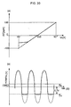
- the control voltage Vc is set to a low level, a desired frequency may not be achieved since the ⁇ f-V-characteristic is not linear.
- the cause of this is that when the control voltage Vc approaches a low level, the capacitance of the varactor Cv increases (the impedance is reduced), and the negative side of the oscillation amplitude is clipped by the forward voltage (approximately -0.7 V) of the varactor Cv.
- Fig. 20(b) shows time on the abscissa and the amplitude of the oscillation signal generated in the oscillator loop on the ordinate.
- the resistor Rs has a fixed value. It is therefore necessary to provide a plurality of IC chips in order that each IC chip has the resistor Rs with a resistance value appropriate for a respective resonator X whose oscillation frequency f may differ from that of other resonators. As a result, the cost is increased.
- Fig. 1 shows the structure of a VCO 10 of a first embodiment.
- the VCO 10 includes a frequency control terminal VC for applying a control voltage Vc for changing the oscillation frequency f of an oscillation signal S outputted from an output terminal OUT; an input resistor Ri, one end of which is connected to the frequency control terminal VC to suppress influence on an oscillation frequency control circuit (not shown), which is to be connected by a user to the frequency control terminal VC; a piezoelectric resonator X, one end of which is connected to the other end of the input resistor Ri; a varactor Cv, the cathode terminal of which is connected to the node between the input resistor Ri and the resonator X; a resistor circuit 20 for adjusting the oscillation frequency, having one end connected to the other end of the resonator X; an oscillator circuit 100 connected to the other end of the resistor circuit 20; a memory 30; and a control circuit 40.
- the components of the VCO 10 other than the resonator X and the varactor Cv are formed as an IC chip 15.
- the IC chip 15, the resonator X, and the varactor Cv are mold-sealed. Terminals exposed to the outside include the frequency control terminal VC; control terminals CNT1 to CNTn; a high-potential power supply terminal VCC; the output terminal OUT; and a low-potential power supply terminal GND.
- the oscillator circuit 100 includes a first bias resistor R1, one end of which is connected to the high-potential power supply terminal VCC, and the other end is connected to the resistor circuit 20; a second bias resistor R2, one end of which is connected to the node between the resistor circuit 20 and the first bias resistor R1, and the other end is connected to the low-potential power supply terminal GND; an NPN transistor Q1, the base terminal of which is connected to the node between the resistor circuit 20 and the first bias resistor R1, and the collector terminal is connected to the terminal VCC; an emitter resistor Re, one end of which is connected to the emitter terminal of the NPN transistor Q1, and the other end is connected to the terminal GND; an NPN transistor Q2, the base terminal of which is connected to the node between the emitter terminal of the NPN transistor Q1 and the emitter resistor Re, and the collector terminal is connected to the terminal VCC; an emitter resistor R0, one end of which is connected to the emitter terminal of the NPN transistor Q2, and the other
- the resistor circuit 20 includes oscillation-amplitude adjusting resistors Rs1 to Rsn and switches SW1 to SWn connected to the oscillation-amplitude adjusting resistors Rs1 to Rsn, respectively.
- the switches SW1 to SWn are for connecting or disconnecting the resistors Rs1 to Rsn, based on resistor connection control signals SC1 to SCn outputted from the control circuit 40.
- the resistance values of the resistors Rs1 to Rsn may differ from one another or may be the same.
- the resistance values of the resistors Rs1 to Rsn are all equal, for example, 100 ⁇
- the resistance of the resistor circuit 20 becomes 100 ⁇ , 50 ⁇ , 33 ⁇ , 25 ⁇ , 20 ⁇ , ...
- an oscillator loop which consists of the resonator X, the varactor Cv, and the oscillator circuit 100, is formed.
- the oscillation amplitude can be controlled.
- the switches SW1 to SWn each have a bipolar transistor structure.
- the switches SW1 to SWn each have a MOS transistor structure.
- the switches SW1 to SWn can have either a bipolar transistor structure as shown in Fig. 3(a) or a MOS transistor structure as shown in Fig. 3(b).
- the MOS transistor structure which does not require a continuous flow of current in order to turn a transistor on and to keep it turned on. Since the MOS transistor is a voltage-controlled device, it is only necessary to apply, to the gate terminal, a voltage at a sufficient level to turn the MOS transistor and to keep it turned on. There is no current flow from the gate terminal to the source terminal side. In contrast, when the bipolar transistor structure is employed, it is necessary that a sufficient current flows between the base terminal and the emitter terminal, in order to reduce the on-resistance of the transistor in a selection state.
- the memory 30 can be formed of a nonvolatile semiconductor memory, such as an EEPROM, which is an electrically erasable type memory, an EPROM, which can be erased by ultraviolet light, a fuse-type ROM, which is a fuse type memory, or the like.
- control data DR for turning on/off the switches SW1 to SWn, in order to set the resistance of the resistor circuit 20, is stored.
- the control data DR is written to the memory 30 through the control circuit 40 prior to factory shipment.
- the resistor connection control signals SC1 to SCn for turning on/off the switches SW1 to SWn are generated by the control circuit 40.
- the control circuit 40 When adjusting the resistance of resistor circuit 20, which is set prior to factory shipment, the control circuit 40 turns on/off the switches SW1 to SWn of the resistor circuit 20 based on a control signal Rcon, which is inputted from the outside through the control terminals CNT1 to CNTn. When adjustment is completed, the control circuit 40 stores the control data DR in the memory 30 based on a resistor confirming signal Dcon. In normal operation, the control circuit 40 generates the control signals SC1 to SCn based on the control data DR stored in the memory 30 and turns on/off the switches SW1 to SWn based on the control signals SC1 to SCn.
- Fig. 4 shows the ⁇ f-V-characteristic for each preset resistance Rsi (i: 1 to n) when the voltage level of a control signal Vconj applied to the frequency control terminal VC is changed from a high level to a low level.
- Fig. 5 shows the amplitude of an oscillation signal in the oscillator loop.
- the resistor circuit 20 connected in the oscillator loop changes the impedance of the oscillator loop, based on the selected resistance from among the resistors Rs1 to Rsn, thereby adjusting the oscillation amplitude.
- the effective resistance of the resistor circuit 20 will be referred to as Rs.
- Fig. 4 shows the variation in the ⁇ f-V-characteristic.
- the ⁇ f-V-characteristic becomes linear.
- the range within the frequency can be changed by the control voltage Vc is increased.
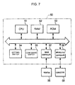
- the adjusting device 50 is formed of a microcomputer.
- the adjusting device 50 includes a CPU 51, a RAM 52, a ROM 53, a switch 54, a confirming switch 55, an image controller 57 connected to a monitor 56, and an input/output controller 59 connected to a connector 58.
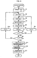
- the ROM 53 is a read-only program memory which stores a resistor setting program such as that shown in Fig. 9 and various parameters for performing the program.
- the CPU 51 executes the program read from the ROM 53 to control signals (the control signal Rcon, the control signal Vcon, etc.) outputted from the input/output controller 59.
- the RAM 52 is used as a work area or the like when the CPU 51 performs the program.
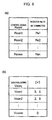
- Various parameters stored in the ROM 53 include values for the control signal Rcon and the control signal Vcon.
- Fig. 8 shows the values that correspond to the various signals.
- Fig. 8(a) shows values that correspond to the control signals Rcon.
- a control signal Rcon1 turns on the switch SW1 of the resistor circuit 20 and connects the resistor Rs1 to the oscillator loop;
- a control signal Rcon2 turns on the switch SW2 of the resistor circuit 20 and connects the resistor Rs2 to the oscillator loop; ...;
- a control signal Rconn turns on the switch SWn of the resistor circuit 20 and connects the resistor Rsn to the oscillator loop.
- Fig. 8(b) shows voltage values that correspond to the control signal Vcon.
- the switch 54 and the confirming switch 55 are for activating the adjusting operation of the adjusting device 50.
- the switch 54 and the confirming switch 55 are provided on a casing (not shown) of the adjusting device 50.
- the confirming switch 55 is operated by the operator by selecting a desired resistor in accordance with the ⁇ f-V-characteristic based on each resistor displayed on the monitor 56.
- the resistor confirming signal Dcon is outputted.
- the CPU 51 transmits the resistor confirming signal Dcon to the control circuit 40, and the control circuit 40 in turn writes the control data DR which corresponds to the confirmed resistor into the memory 30.
- the resistance values of the resistors Rs1 to Rsn forming the resistor circuit 20 are, for example, 10 ⁇ , 20 ⁇ , ..., 100 ⁇ , respectively.
- the operator connects the VCO 10 to the connector 58 of the adjusting device 50 and turns on the switch 54.
- the CPU 51 reads the resistor setting program and various parameters (the values for the control signals Rcon and the values for the control signals Vcon) which are stored in the ROM 53 into the RAM 52.
- the CPU 51 starts a resistor setting process in accordance with the resistor setting program.
- the CPU 51 reads the value for control signal Rcon1 from the parameters stored in the RAM 52 and supplies the control signal Rcon1 to the control terminal CNT1 through the input/output controller 59 and the connector 58 (step S2).
- control circuit 40 of the VCO 10 turns on the switch SW1 of the resistor circuit 20 and connects the resistor Rs1 to the oscillator loop.
- the CPU 51 reads the voltage value for control signal Vcon1 (for example 3V) from the parameters stored in the RAM 52 and applies the corresponding voltage as control signal Vcon1 to the frequency control terminal VC, through the input/output controller 59 and the connector 58 (step S3).
- Vcon1 for example 3V
- the resistor Rs1 adjusts the oscillation amplitude of the oscillator loop, and subsequently the capacitance of the varactor Cv is changed by the applied control signal Vcon1.
- the oscillation signal S which has a oscillation frequency f1 determined by the resonance with the resonator X, is outputted.
- the CPU 51 determines whether or not the index j has reached m (step S7). If the index j has not reached m (NO in step S7), it means that the measurement of the frequency deviation ⁇ fj has not been completed, in which the control voltage Vc is gradually decreased from 3V to 0.1V, while the resistor circuit 20 is set to resistor Rs1. Thus, the process proceeds to step S8.
- the CPU 51 repeats the processing from step S3 to step S8 until the determination in step S7 becomes affirmative. Every time the processing is repeated, the CPU 51 stores the frequency deviation ⁇ fj in correspondence with j in the RAM 52.
- step S7 the CPU 51 determines whether or not the index i has reached n (step S9). If the index i has not reached n (NO in step S9), it means that the measurement of the frequency deviation ⁇ fj has not been completed, in which the control signal Vconj is gradually decreased from 3V to 0.1V for each of the resistors Rs1 to Rsn of the resistor circuit 20. Thus, the process proceeds to step S10.
- the CPU 51 repeats the processing from step S2 to S9 until the determination in step S9 becomes affirmative. Every time step S6 is performed, the CPU 51 sequentially stores the frequency deviation ⁇ fj in correspondence with the resistor Rsj in the RAM 52.
- step S9 the CPU 51 determines that the measurement of the frequency deviation ⁇ fj has been completed for all combinations of control signals Vconj and control signals Rcon.
- the CPU 51 reads the frequency deviation ⁇ fj stored in the RAM 52 and displays, as shown in Fig. 4, the ⁇ f-V-characteristic for each resistor on the monitor 56 through the image controller 57 (step S11).
- the operator looks at the ⁇ f-V-characteristic for each resistor and operates the confirming switch 55 so as to select a desired resistance. Accordingly, the CPU 51 reads the resistor confirming signal Dcon in response to the operation of the confirming switch 55 (step S12).
- the CPU 51 transfers the resistor confirming signal Dcon, which is to turn on switch SWi corresponding to the resistor Rsi, to the control circuit 40 through the input/output controller 59 and the connector 58 (step S13).
- the control circuit 40 stores the control data DR for connecting the confirmed resistor Rsi to the oscillator loop.
- the appropriate resistor Rsi of the resistor circuit 20 can be selected and confirmed easily.
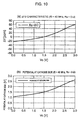
- Figs. 10(a), 11(a), 12(a), and 13(a) the ⁇ f-V-characteristic in accordance with conditions concerning the reference frequency f0 and the resistance Rs of the resistor circuit 20 are shown.
- Figs. 10(b), 11(b), 12(b), and 13(b) the potential (oscillation amplitude) at the cathode side versus the control voltage Vc (V-V-characteristic) is shown.
- the resistance values of the resistors Rs1 to Rsn of the resistor circuit 20 are 10 ⁇ , 20 ⁇ , ..., 100 ⁇ , respectively.
- the V-V-characteristic loses linearity when the control voltage Vc is approximately 1.7 V. Accordingly, the ⁇ f-V-characteristic loses linearity when the control voltage Vc is approximately 1.7 V.
- the frequency can be changed by the control voltage Vc within a range from + 10 to 60 ppm.
- the resistance Rs of the resistor circuit 20 is set to 100 ⁇ , as shown in Fig. 11, the potential at the cathode side changes linearly with a change in Vc. Accordingly, the ⁇ f-V-characteristic is also linear. Thus, the frequency can be changed by the control voltage Vc within a range of ⁇ 70 ppm.
- the V-V-characteristic loses linearity when the control voltage Vc is approximately 0.5 V. Accordingly, the ⁇ f-V-characteristic also loses linearity when the control voltage Vc is approximately 0.5 V.
- the frequency can be changed by the control voltage Vc within a range from -40 to 65 ppm.
- the resistance Rs of the resistor circuit 20 is set to 30 ⁇ , as shown in Fig. 13, the potential at the cathode side changes linearly with Vc. Accordingly, the ⁇ f-V-characteristic is linear. Thus, the frequency can be changed by the control voltage Vc within a range of ⁇ 70 ppm.
- the resistance of the resistors Rs1 to Rsn which form the resistor circuit 20 are 10 ⁇ to 100 ⁇ , respectively, and the resistor circuit 20 is incorporated into the IC chip 15. Accordingly, the same IC chip 15 can handle different resonators X with different oscillation frequencies f. For the same reason, the same IC chip 15 can handle various oscillation frequencies f, and the cost is greatly reduced.
- the resistor circuit 20 which can change the impedance of the oscillator loop, is connected to the oscillator loop.
- An appropriate one is selected from among the resistors Rs1 to Rsn of the resistor circuit 20 in order to make the oscillation amplitude smaller than the forward voltage of the varactor Cv, thereby preventing the oscillation amplitude from being clipped by the forward voltage.
- the control voltage Vc is set to a low level
- a change in capacitance of the varactor Cv has correspondence with the control voltage Vc.
- the range of the ⁇ f-V-characteristic within which the frequency can be changed linearly by the control voltage VC is increased.
- the VCO 10 includes the memory 30 and the control circuit 40, the resistor of the resistor circuit 20 can be confirmed after the VCO 10 is assembled. Also, the adjustment of frequency variable range can be changed in accordance with a request from a user.
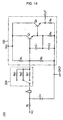
- Fig. 14 a diagram showing the principle of a second embodiment is illustrated.
- the same reference numerals are given to components corresponding to those in the first embodiment, and a repeated description of the common portions is omitted.
- the VCO 10A of the second embodiment is characterized in that a structure is employed which, instead of using semiconductor devices to form the switches SW1 to SWn of the resistor circuit 20, uses bonding wires to connect bonding pads exposed on the IC chip 15 to lands on a board, and selects the resistor (so-called bonding option).
- the components other than the resonator X and the varactor Cv are formed as an IC chip.
- bonding option pads for (confirming) selecting the one or more of the resistors Rs1 to Rsn are formed.
- the pads and the lands are connected to each other by the bonding wires in order to select the resistors prior to mold-sealing and assembling the IC chip, the resonator X, and the varactor Cv.
- the appropriate resistor(s) is (are) appropriately confirmed, and hence the linear region of the ⁇ f-V-characteristic is expanded. As a result, the range of frequencies that can be varied linearly by the control voltage Vc is increased.
- the VCO 10A does not include the memory 30 and the control circuit 40, the area of the IC chip is minimized, and the number of components is reduced.
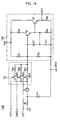
- Fig. 15 a diagram showing the principle of a third embodiment is illustrated.
- the same reference numerals are given to components corresponding to those in the first embodiment, and a repeated description of the common portions is omitted.
- the VCO 10B of the third embodiment is characterized in that control terminals CNT1' to CNTn', to which a control voltage for activating the switches SW1 to SWn is applied, are exposed to the outside of the IC.
- the control voltage applied from the outside through the control terminals CNT1' to CNTn' is used to select the resistor Rs.
- the resistor is appropriately selected by a selection signal from the outside, and hence the range of frequencies that can be varied linearly by the control voltage Vc is increased.
- the VCO 10B does not include the memory 30 and the control circuit 40, the area of the IC chip is minimized, and the number of components is reduced.
- a frequency setting circuit 21 can be connected to the anode side of the varactor Cv.
- the frequency setting circuit 21 includes a base capacitor Cg which functions as a fixed-capacitance element, n capacitors Ca1 to Can which function as selectable-capacitance elements, and switches SW1' to SWn' which connect the capacitors Ca1 to Can in parallel.
- a block diagram of the VCO of this modification is shown.
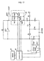
- This VCO differs from the foregoing embodiments in that a CMOS oscillator circuit including a CMOS inverter INV is used as the oscillator circuit and that a resistor circuit 20, similar to that of the first embodiment, is applied to the CMOS oscillator circuit.
- a resistor circuit 20 similar to that of the first embodiment, is applied to the CMOS oscillator circuit.
- the reference frequency f0 By connecting the frequency setting circuit 21 of the first modification, the reference frequency f0 can be adjusted.
- the components other than the resonator X and the varactor Cv are formed as the IC chip 15, and the IC chip 15, the resonator X, and the varactor Cv are mold-sealed.
- the present invention is not limited to this structure.
- the components (including the varactor Cv) other than the resonator X are formed as an IC chip 16, and the IC chip 16 and the resonator X can be mold-sealed.
- the operator monitors the ⁇ f-V-characteristics and thereafter confirms the desired resistor.
- the present invention is not limited to this embodiment. By determining whether or not a differential value obtained by differentiating the measured frequency deviation ⁇ f exceeds a threshold value, the resistor can be automatically confirmed. As long as the linearity of ⁇ f-V-characteristic is improved, any method for confirming the resistor can be used.
- the range of frequency that can be varied by the control voltage Vc is increased by improving the linearity of ⁇ f-V-characteristic.
- the control voltage Vc is Vc1 or greater as a range in which the frequency can be changed, and a region in which the control voltage Vc is Vc1 or smaller as a range in which the frequency does not vary.
- the linearity of ⁇ f-V-characteristic can be improved, and the range of frequency that can be varied by a control voltage can be increased.
Landscapes
- Oscillators With Electromechanical Resonators (AREA)
- Inductance-Capacitance Distribution Constants And Capacitance-Resistance Oscillators (AREA)
Abstract
Description
- Fig. 1
- is a diagram showing the principle of a VCO of a first embodiment.
- Fig. 2
- is a perspective view of the VCO of the first embodiment.
- Fig. 3
- illustrates cases when switches are formed of semiconductor devices.
- Fig. 4
- is a graph showing a Δf-V-characteristic of the first embodiment.
- Fig. 5
- is a graph showing oscillation amplitude of the first embodiment.
- Fig. 6
- is a circuit diagram showing the VCO of the first embodiment to which an adjusting device is connected.
- Fig. 7
- is a block diagram of the structure of the adjusting device.
- Fig. 8
- illustrates the correspondence concerning signals included in the adjusting device.
- Fig. 9
- is a flowchart showing a resistor setting process performed by the adjusting device.
- Fig. 10
- includes graphs showing a Δf-V-characteristic and potentials at the cathode side of an example (f0 = 40 MHz and Rs = 0 Ω) of the first embodiment.
- Fig. 11
- includes graphs showing a Δf-V-characteristic and potentials at the cathode side of an example (f0 = 40 MHz and Rs = 100 Ω) of the first embodiment.
- Fig. 12
- includes graphs showing a Δf-V-characteristic and potentials at the cathode side of an example (f0 = 80 MHz and Rs = 0 Ω) of the first embodiment.
- Fig. 13
- includes graphs showing a Δf-V-characteristic and potentials at the cathode side of an example (f0 = 80 MHz and Rs = 30 Ω) of the first embodiment.
- Fig. 14
- is a circuit diagram of a VCO of a second embodiment.
- Fig. 15
- is a circuit diagram of a VCO of a third embodiment.
- Fig. 16
- is a circuit diagram of a VCO of a first modification.
- Fig. 17
- is a circuit diagram of a VCO of a second modification.
- Fig. 18
- is a perspective view of a VCO of a third modification.
- Fig. 19
- is a circuit diagram of a VCO of the related art.
- Fig. 20
- includes graphs showing a Δf-V-characteristic and oscillation amplitude of the related art.
- Fig. 21
- is a circuit diagram of an equivalent circuit of a piezoelectric resonator.
Claims (20)
- A voltage-controlled oscillator comprising:a piezoelectric resonator (X);a variable reactance element (Cv) connected in series to the input side of said resonator (X);an oscillator circuit (100) connected to said variable reactance element (Cv); anda resistor circuit (20) provided in an oscillator loop including said resonator (X), said variable reactance element (Cv), and said oscillator circuit (100), said resistor circuit (20) comprising a plurality of resistors (Rs1-Rsn) which are selectively inserted.
- The oscillator according to Claim 1, wherein said resistor circuit (20) comprises switch means (SW1-SWn) for connecting or disconnecting the resistors (Rs1-Rsn) based on a first control signal (SC1-SCn).
- The oscillator according to Claim 2, wherein said switch means (SW1-SWn) comprises a semiconductor switches.
- The oscillator according to Claim 2 or 3, further comprising:a memory (30) for storing control data; anda control circuit (40) for storing the control data beforehand in said memory (30), based on a second control signal (Vcon1-Vconm) which is supplied from the outside, and for outputting said first control signal (SC1-SCn) for controlling said switch means (SW1-SWn) based on said second control signal (Vcon1-Vconm) or the control data.
- The oscillator according to Claim 1, wherein said resistor circuit (20) has one end of each of its resistors (Rs1-Rsn) connected to the oscillator loop and the other end connected to a bonding pad.
- The oscillator according to any one of the preceding Claims, further comprising;a capacitor circuit (21) connected to said variable reactance element (Cv), said capacitor circuit comprising a plurality of selectable capacitance elements (Caj1-Cajn); anda capacitance connecting circuit (SW1'-SWn') for connecting to said variable reactance element (Cv) a desired capacitive element from among the selectable capacitance elements (Caj1-Cajn).
- The oscillator according to any one of the preceding Claims, wherein said resonator (X) is a crystal resonator.
- The oscillator according to any one of the preceding Claim, wherein components other than said resonator (X) and said variable reactance element (Cv) are formed as an IC chip (15).
- The oscillator according to Claim 8, wherein said IC chip (15), said resonator (X), and said variable reactance element (Cv) are integrally mold-sealed.
- The oscillator according to Claim 8, wherein said IC chip (15), said resonator (X), and said variable reactance element (Cv) are contained in a single package.
- The oscillator according to Claim 8, wherein said resonator (X) and said variable reactance element (Cv) are integrally mold-sealed.
- The oscillator according to Claim 8, wherein said resonator (X) and said variable reactance element (Cv) are contained in a single package.
- The oscillator according to any one of the preceding Claims, wherein components other than said resonator (X) are formed as an IC chip (16).
- The oscillator according to Claim 13, wherein said IC chip (16) and said resonator (X) are integrally mold-sealed.
- The oscillator according to Claim 13, wherein said IC chip (16) and said resonator (X) are contained in a single package.
- An IC chip for a voltage-controlled oscillator, said voltage-controlled oscillator including:a piezoelectric resonator (X);a variable reactance element (Cv) connected in series to the input side of said resonator (X); andan oscillator circuit (100) connected to said variable reactance circuit;said IC chip (15; 16) comprising a resistor circuit (20) provided in an oscillator loop including said resonator (X), said variable reactance element (Cv), and said oscillator circuit (100), said resistor circuit (20) comprising a plurality of resistors (Rs1-Rsn) which are selectively inserted.
- An apparatus for selecting a desired one of said resistors (Rs1-Rsn) in a voltage-controlled oscillator as set forth in any one of Claims 1 to 15, said resistance setting apparatus comprising:frequency detecting means for sequentially selecting each of said resistors (Rs1-Rsn), one at a time, and detecting with the respectively selected resistor (Rs1-Rsn) at each of predetermined reference control voltages sequentially applied to a control voltage terminal (VC), the frequency of an oscillation signal; andconfirming means for confirming the desired resistor (Rs1-Rsn) which corresponds to a predetermined oscillation frequency, based on the detected frequencies for each resistor (Rs1-Rsn).
- An apparatus for selecting a desired one of said resistors (Rs1-Rsn) in a voltage-controlled oscillator as set forth in any one of Claims 1 to 15, said resistance setting apparatus comprising:frequency detecting means for sequentially selecting each of said resistors (Rs1-Rsn), one at a time, and detecting with the respectively selected resistor (Rs1-Rsn) at each of predetermined reference control voltages sequentially applied to a control voltage terminal (VC), the frequency of an oscillation signal;characteristics generating means for generating a frequency change versus control voltage characteristic for each resistor (Rs1-Rsn), based on the frequencies detected with that resistor; andconfirming means for confirming the desired resistor (Rs1-Rsn) which corresponds to a predetermined oscillation frequency, based on the generated frequency change versus control voltage characteristic for each resistor.
- A method of selecting a desired one of said resistors (Rs1-Rsn) in a voltage-controlled oscillator as set forth in any one of Claims 1 to 15, said method comprising:(a) sequentially selecting one of said resistors (Rs1-Rsn) and detecting with the respectively selected resistor (Rs1-Rsn) at each of predetermined reference control voltages sequentially applied to a control voltage terminal (VC), the frequency of an oscillation signal; and(b) confirming the desired resistor which corresponds to a predetermined oscillation frequency, based on the frequencies detected for each resistor (Rs1-Rsn) in step (a).
- A method of selecting a desired one of said resistors (Rs1-Rsn) in a voltage-controlled oscillator as set forth in any one of Claims 1 to 15, said method comprising:(a) sequentially selecting one of said resistors (Rs1-Rsn) and detecting with the respectively selected resistor (Rs1-Rsn) at each of predetermined reference control voltages sequentially applied to a control voltage terminal (VC), the frequency of an oscillation signal;(b) generating a frequency change versus control voltage characteristic for each resistor, based on the frequencies detected for that resistor in step (a); and(c) confirming the desired resistor, based on the characteristics generated in step (b).
Applications Claiming Priority (2)
| Application Number | Priority Date | Filing Date | Title |
|---|---|---|---|
| JP2000259870A JP3593963B2 (en) | 2000-08-29 | 2000-08-29 | Voltage controlled oscillator, IC chip for voltage controlled oscillator, resistance adjusting device and resistance adjusting method |
| JP2000259870 | 2000-08-29 |
Publications (3)
| Publication Number | Publication Date |
|---|---|
| EP1187309A2 true EP1187309A2 (en) | 2002-03-13 |
| EP1187309A3 EP1187309A3 (en) | 2003-01-22 |
| EP1187309B1 EP1187309B1 (en) | 2010-07-07 |
Family
ID=18747981
Family Applications (1)
| Application Number | Title | Priority Date | Filing Date |
|---|---|---|---|
| EP01119839A Expired - Lifetime EP1187309B1 (en) | 2000-08-29 | 2001-08-16 | Voltage-controlled oscillator, IC chip for voltage-controlled oscillator, resistance setting apparatus, and resistance setting method |
Country Status (4)
| Country | Link |
|---|---|
| US (1) | US6577203B2 (en) |
| EP (1) | EP1187309B1 (en) |
| JP (1) | JP3593963B2 (en) |
| DE (1) | DE60142503D1 (en) |
Families Citing this family (11)
| Publication number | Priority date | Publication date | Assignee | Title |
|---|---|---|---|---|
| JP2002344242A (en) * | 2001-05-18 | 2002-11-29 | Nippon Precision Circuits Inc | Voltage-controlled oscillator |
| JP3973910B2 (en) * | 2002-01-21 | 2007-09-12 | シチズンホールディングス株式会社 | Method for manufacturing temperature compensated oscillator |
| US7088192B2 (en) * | 2003-03-31 | 2006-08-08 | Toyo Communication Equipment Co., Ltd. | Inverter oscillator circuit |
| US7266349B2 (en) * | 2004-08-06 | 2007-09-04 | Broadcom Corporation | Multi-mode crystal oscillator |
| CN100452844C (en) * | 2005-12-02 | 2009-01-14 | 邓明友 | Audio and video wireless transmitting device |
| US8816786B2 (en) * | 2012-10-01 | 2014-08-26 | Tensorcom, Inc. | Method and apparatus of a crystal oscillator with a noiseless and amplitude based start up control loop |
| JP6350793B2 (en) * | 2013-12-25 | 2018-07-04 | セイコーエプソン株式会社 | OSCILLATOR CIRCUIT, OSCILLATOR, ELECTRONIC DEVICE, MOBILE BODY, AND OSCILLATOR MANUFACTURING METHOD |
| JP2016019131A (en) * | 2014-07-08 | 2016-02-01 | 日本電波工業株式会社 | Voltage-controlled oscillator |
| US9520823B2 (en) * | 2014-10-22 | 2016-12-13 | Semiconductor Components Industries, Llc | Control circuit and method |
| CN106330097B (en) * | 2016-08-19 | 2019-02-19 | 西安电子科技大学 | InP HBT Voltage Controlled Oscillator Based on Coupled Transmission Line |
| IT201900005268A1 (en) | 2019-04-05 | 2020-10-05 | Wise S R L | Device for electrotherapy and / or electrophysiology, kit and assembly |
Family Cites Families (8)
| Publication number | Priority date | Publication date | Assignee | Title |
|---|---|---|---|---|
| US4607239A (en) * | 1985-02-28 | 1986-08-19 | The United States Of America As Represented By The Secretary Of The Army | Adjustment of the frequency-temperature characteristics of crystal oscillators |
| FR2621187A1 (en) * | 1987-09-29 | 1989-03-31 | Cepe | TEMPERATURE COMPENSATED PIEZOELECTRIC OSCILLATOR |
| GB9027738D0 (en) | 1990-12-20 | 1991-02-13 | Stc Plc | Crystal oscillator |
| JPH07240629A (en) | 1994-03-01 | 1995-09-12 | Kinseki Ltd | Voltage controlled piezoelectric oscillator |
| JPH104318A (en) * | 1996-04-15 | 1998-01-06 | Mitsumi Electric Co Ltd | Temperature compensated crystal oscillator |
| DE19621228A1 (en) | 1996-05-25 | 1997-11-27 | Itt Ind Gmbh Deutsche | Digitally adjustable quartz oscillator with monolithically integrated oscillator circuit |
| JPH10335937A (en) | 1997-05-30 | 1998-12-18 | Nippon Dempa Kogyo Co Ltd | Voltage controlled crystal oscillation circuit |
| US6078226A (en) * | 1998-02-02 | 2000-06-20 | Tritech Microelectronics, Ltd. | Integrated circuit implementation of a frequency shift keying oscillator |
-
2000
- 2000-08-29 JP JP2000259870A patent/JP3593963B2/en not_active Expired - Fee Related
-
2001
- 2001-08-09 US US09/924,514 patent/US6577203B2/en not_active Expired - Lifetime
- 2001-08-16 EP EP01119839A patent/EP1187309B1/en not_active Expired - Lifetime
- 2001-08-16 DE DE60142503T patent/DE60142503D1/en not_active Expired - Lifetime
Also Published As
| Publication number | Publication date |
|---|---|
| US20020024397A1 (en) | 2002-02-28 |
| JP2002076771A (en) | 2002-03-15 |
| JP3593963B2 (en) | 2004-11-24 |
| US6577203B2 (en) | 2003-06-10 |
| EP1187309B1 (en) | 2010-07-07 |
| EP1187309A3 (en) | 2003-01-22 |
| DE60142503D1 (en) | 2010-08-19 |
Similar Documents
| Publication | Publication Date | Title |
|---|---|---|
| US5473289A (en) | Temperature compensated crystal oscillator | |
| EP1187309A2 (en) | Voltage-controlled oscillator, IC chip for voltage-controlled oscillator, resistance setting apparatus, and resistance setting method | |
| KR960016733B1 (en) | Oscillation circuit | |
| US7205858B2 (en) | Temperature compensated piezoelectric oscillator and electronic apparatus comprising it | |
| US6861915B2 (en) | Crystal oscillator with adjustable capacitive assembly having selectable capacitances | |
| US6480071B1 (en) | Piezoelectric oscillator and electronic device | |
| US6788158B2 (en) | Piezoelectric oscillator, method of producing the same, and electronic device using the piezoelectric oscillator | |
| EP1471632A2 (en) | Oscillator circuit and oscillator | |
| US6617756B1 (en) | Piezo-oscillator | |
| JP2003283249A (en) | Crystal oscillation circuit and electronic equipment using the crystal oscillation circuit | |
| US7268636B2 (en) | Voltage controlled oscillator | |
| JPH0645826A (en) | Voltage controlled oscillator | |
| JP3536665B2 (en) | Voltage controlled piezoelectric oscillator adjustment system and voltage controlled piezoelectric oscillator adjustment method | |
| JPH0846427A (en) | Voltage controlled crystal oscillator | |
| JP2005217773A (en) | Voltage controlled piezoelectric oscillator | |
| JPH1056330A (en) | Voltage controlled piezoelectric oscillator | |
| JP3446602B2 (en) | Piezoelectric oscillator, oscillator adjustment system, and oscillator adjustment method | |
| JPH07273547A (en) | Voltage controlled inverter oscillator circuit | |
| JP2007019565A (en) | Crystal oscillator | |
| US11689159B2 (en) | Circuit device and oscillator | |
| JP2000183650A (en) | Piezoelectric oscillator | |
| JP3325732B2 (en) | Voltage controlled piezoelectric oscillator | |
| US7098750B2 (en) | Wide frequency range agile voltage controlled oscillator | |
| JP2002359521A (en) | Frequency switching crystal oscillator | |
| JP2003258553A (en) | Oscillation circuit |
Legal Events
| Date | Code | Title | Description |
|---|---|---|---|
| PUAI | Public reference made under article 153(3) epc to a published international application that has entered the european phase |
Free format text: ORIGINAL CODE: 0009012 |
|
| AK | Designated contracting states |
Kind code of ref document: A2 Designated state(s): AT BE CH CY DE DK ES FI FR GB GR IE IT LI LU MC NL PT SE TR |
|
| AX | Request for extension of the european patent |
Free format text: AL;LT;LV;MK;RO;SI |
|
| PUAL | Search report despatched |
Free format text: ORIGINAL CODE: 0009013 |
|
| AK | Designated contracting states |
Kind code of ref document: A3 Designated state(s): AT BE CH CY DE DK ES FI FR GB GR IE IT LI LU MC NL PT SE TR |
|
| AX | Request for extension of the european patent |
Free format text: AL;LT;LV;MK;RO;SI |
|
| 17P | Request for examination filed |
Effective date: 20030415 |
|
| AKX | Designation fees paid |
Designated state(s): DE FR GB |
|
| 17Q | First examination report despatched |
Effective date: 20031128 |
|
| 17Q | First examination report despatched |
Effective date: 20031128 |
|
| GRAP | Despatch of communication of intention to grant a patent |
Free format text: ORIGINAL CODE: EPIDOSNIGR1 |
|
| GRAS | Grant fee paid |
Free format text: ORIGINAL CODE: EPIDOSNIGR3 |
|
| GRAA | (expected) grant |
Free format text: ORIGINAL CODE: 0009210 |
|
| AK | Designated contracting states |
Kind code of ref document: B1 Designated state(s): DE FR GB |
|
| REG | Reference to a national code |
Ref country code: GB Ref legal event code: FG4D |
|
| REF | Corresponds to: |
Ref document number: 60142503 Country of ref document: DE Date of ref document: 20100819 Kind code of ref document: P |
|
| PLBE | No opposition filed within time limit |
Free format text: ORIGINAL CODE: 0009261 |
|
| STAA | Information on the status of an ep patent application or granted ep patent |
Free format text: STATUS: NO OPPOSITION FILED WITHIN TIME LIMIT |
|
| 26N | No opposition filed |
Effective date: 20110408 |
|
| REG | Reference to a national code |
Ref country code: DE Ref legal event code: R097 Ref document number: 60142503 Country of ref document: DE Effective date: 20110408 |
|
| REG | Reference to a national code |
Ref country code: FR Ref legal event code: PLFP Year of fee payment: 16 |
|
| PGFP | Annual fee paid to national office [announced via postgrant information from national office to epo] |
Ref country code: DE Payment date: 20160809 Year of fee payment: 16 Ref country code: GB Payment date: 20160810 Year of fee payment: 16 |
|
| PGFP | Annual fee paid to national office [announced via postgrant information from national office to epo] |
Ref country code: FR Payment date: 20160712 Year of fee payment: 16 |
|
| REG | Reference to a national code |
Ref country code: DE Ref legal event code: R119 Ref document number: 60142503 Country of ref document: DE |
|
| GBPC | Gb: european patent ceased through non-payment of renewal fee |
Effective date: 20170816 |
|
| REG | Reference to a national code |
Ref country code: FR Ref legal event code: ST Effective date: 20180430 |
|
| PG25 | Lapsed in a contracting state [announced via postgrant information from national office to epo] |
Ref country code: GB Free format text: LAPSE BECAUSE OF NON-PAYMENT OF DUE FEES Effective date: 20170816 Ref country code: DE Free format text: LAPSE BECAUSE OF NON-PAYMENT OF DUE FEES Effective date: 20180301 |
|
| PG25 | Lapsed in a contracting state [announced via postgrant information from national office to epo] |
Ref country code: FR Free format text: LAPSE BECAUSE OF NON-PAYMENT OF DUE FEES Effective date: 20170831 |