EP1186034B1 - Robust interconnect structure - Google Patents
Robust interconnect structure Download PDFInfo
- Publication number
- EP1186034B1 EP1186034B1 EP00931376A EP00931376A EP1186034B1 EP 1186034 B1 EP1186034 B1 EP 1186034B1 EP 00931376 A EP00931376 A EP 00931376A EP 00931376 A EP00931376 A EP 00931376A EP 1186034 B1 EP1186034 B1 EP 1186034B1
- Authority
- EP
- European Patent Office
- Prior art keywords
- layer
- copper
- alcu
- thick
- pad
- Prior art date
- Legal status (The legal status is an assumption and is not a legal conclusion. Google has not performed a legal analysis and makes no representation as to the accuracy of the status listed.)
- Expired - Lifetime
Links
Images
Classifications
-
- H—ELECTRICITY
- H10—SEMICONDUCTOR DEVICES; ELECTRIC SOLID-STATE DEVICES NOT OTHERWISE PROVIDED FOR
- H10W—GENERIC PACKAGES, INTERCONNECTIONS, CONNECTORS OR OTHER CONSTRUCTIONAL DETAILS OF DEVICES COVERED BY CLASS H10
- H10W20/00—Interconnections in chips, wafers or substrates
- H10W20/40—Interconnections external to wafers or substrates, e.g. back-end-of-line [BEOL] metallisations or vias connecting to gate electrodes
-
- H—ELECTRICITY
- H10—SEMICONDUCTOR DEVICES; ELECTRIC SOLID-STATE DEVICES NOT OTHERWISE PROVIDED FOR
- H10W—GENERIC PACKAGES, INTERCONNECTIONS, CONNECTORS OR OTHER CONSTRUCTIONAL DETAILS OF DEVICES COVERED BY CLASS H10
- H10W72/00—Interconnections or connectors in packages
- H10W72/01—Manufacture or treatment
- H10W72/012—Manufacture or treatment of bump connectors, dummy bumps or thermal bumps
-
- H—ELECTRICITY
- H10—SEMICONDUCTOR DEVICES; ELECTRIC SOLID-STATE DEVICES NOT OTHERWISE PROVIDED FOR
- H10W—GENERIC PACKAGES, INTERCONNECTIONS, CONNECTORS OR OTHER CONSTRUCTIONAL DETAILS OF DEVICES COVERED BY CLASS H10
- H10W72/00—Interconnections or connectors in packages
- H10W72/20—Bump connectors, e.g. solder bumps or copper pillars; Dummy bumps; Thermal bumps
- H10W72/221—Structures or relative sizes
-
- H—ELECTRICITY
- H10—SEMICONDUCTOR DEVICES; ELECTRIC SOLID-STATE DEVICES NOT OTHERWISE PROVIDED FOR
- H10W—GENERIC PACKAGES, INTERCONNECTIONS, CONNECTORS OR OTHER CONSTRUCTIONAL DETAILS OF DEVICES COVERED BY CLASS H10
- H10W72/00—Interconnections or connectors in packages
- H10W72/20—Bump connectors, e.g. solder bumps or copper pillars; Dummy bumps; Thermal bumps
- H10W72/251—Materials
-
- H—ELECTRICITY
- H10—SEMICONDUCTOR DEVICES; ELECTRIC SOLID-STATE DEVICES NOT OTHERWISE PROVIDED FOR
- H10W—GENERIC PACKAGES, INTERCONNECTIONS, CONNECTORS OR OTHER CONSTRUCTIONAL DETAILS OF DEVICES COVERED BY CLASS H10
- H10W72/00—Interconnections or connectors in packages
- H10W72/20—Bump connectors, e.g. solder bumps or copper pillars; Dummy bumps; Thermal bumps
- H10W72/251—Materials
- H10W72/252—Materials comprising solid metals or solid metalloids, e.g. PbSn, Ag or Cu
-
- H—ELECTRICITY
- H10—SEMICONDUCTOR DEVICES; ELECTRIC SOLID-STATE DEVICES NOT OTHERWISE PROVIDED FOR
- H10W—GENERIC PACKAGES, INTERCONNECTIONS, CONNECTORS OR OTHER CONSTRUCTIONAL DETAILS OF DEVICES COVERED BY CLASS H10
- H10W72/00—Interconnections or connectors in packages
- H10W72/20—Bump connectors, e.g. solder bumps or copper pillars; Dummy bumps; Thermal bumps
- H10W72/29—Bond pads specially adapted therefor
-
- H—ELECTRICITY
- H10—SEMICONDUCTOR DEVICES; ELECTRIC SOLID-STATE DEVICES NOT OTHERWISE PROVIDED FOR
- H10W—GENERIC PACKAGES, INTERCONNECTIONS, CONNECTORS OR OTHER CONSTRUCTIONAL DETAILS OF DEVICES COVERED BY CLASS H10
- H10W72/00—Interconnections or connectors in packages
- H10W72/90—Bond pads, in general
- H10W72/921—Structures or relative sizes of bond pads
- H10W72/923—Bond pads having multiple stacked layers
-
- H—ELECTRICITY
- H10—SEMICONDUCTOR DEVICES; ELECTRIC SOLID-STATE DEVICES NOT OTHERWISE PROVIDED FOR
- H10W—GENERIC PACKAGES, INTERCONNECTIONS, CONNECTORS OR OTHER CONSTRUCTIONAL DETAILS OF DEVICES COVERED BY CLASS H10
- H10W72/00—Interconnections or connectors in packages
- H10W72/90—Bond pads, in general
- H10W72/941—Dispositions of bond pads
- H10W72/9415—Dispositions of bond pads relative to the surface, e.g. recessed, protruding
-
- H—ELECTRICITY
- H10—SEMICONDUCTOR DEVICES; ELECTRIC SOLID-STATE DEVICES NOT OTHERWISE PROVIDED FOR
- H10W—GENERIC PACKAGES, INTERCONNECTIONS, CONNECTORS OR OTHER CONSTRUCTIONAL DETAILS OF DEVICES COVERED BY CLASS H10
- H10W72/00—Interconnections or connectors in packages
- H10W72/90—Bond pads, in general
- H10W72/951—Materials of bond pads
- H10W72/952—Materials of bond pads comprising metals or metalloids, e.g. PbSn, Ag or Cu
-
- H—ELECTRICITY
- H10—SEMICONDUCTOR DEVICES; ELECTRIC SOLID-STATE DEVICES NOT OTHERWISE PROVIDED FOR
- H10W—GENERIC PACKAGES, INTERCONNECTIONS, CONNECTORS OR OTHER CONSTRUCTIONAL DETAILS OF DEVICES COVERED BY CLASS H10
- H10W74/00—Encapsulations, e.g. protective coatings
- H10W74/10—Encapsulations, e.g. protective coatings characterised by their shape or disposition
- H10W74/131—Encapsulations, e.g. protective coatings characterised by their shape or disposition the semiconductor body being only partially enclosed
- H10W74/147—Encapsulations, e.g. protective coatings characterised by their shape or disposition the semiconductor body being only partially enclosed the encapsulations being multilayered
Definitions
- the present invention relates to metal interconnects and more particularly to a robust copper interconnect structure.
- the present invention finds particular applicability for VLSI and ULSI copper interconnects especially for packaging.
- capping of the copper is essential.
- the capping inhibits this diffusion.
- One widely suggested method of capping includes employing a conductive barrier layer along the sidewalls and bottom surface of a copper interconnect. Typical of such barrier layers is tantalum or titanium. Capping of the upper surface of a copper interconnect usually employs silicon nitride.
- silicon nitride does not exhibit strong adhesion to copper surfaces despite various adhesion treatments. Accordingly, the silicon nitride-to-copper interface is susceptible to delamination under conditions of mechanical loading.
- US-A-5 898 222 describes capped copper electrical interconnects comprising a copper wiring layer which is capped with a material selected from a group including Ni and Al, the capping layer being said to provide improved adhesion and passivation.
- a structure comprising layer of copper, a barrier layer, a layer of AlCu and a pad-limiting layer, wherein the layer of AlCu and barrier layer are interposed between the layer of copper and pad-limiting layer, and wherein the barrier layer is located between the layer of copper and the layer of AlCu.
- the present embodiment provides for improved structural integrity of copper interconnects including C4 over copper BEOL.
- the present invention provides for interconnect that is robust to mechanical stresses.
- the layer of copper may be about 3.0 to about 2 ⁇ m thick.
- the structure of the present invention comprises a layer of copper, a pad limiting layer and a layer of AlCu and barrier interposed between the layer of copper and pad-limiting layer.
- the present embodiments also relates to an interconnect structure comprising a layer of copper, a capping layer located over the layer of copper and having a via to expose a portion of the layer of copper, a barrier layer located in the via and over the layer of copper, a layer of AlCu located over the barrier layer, and a pad-limiting layer located over the layer of AlCu.
- the barrier layer may overlap portions of the dielectric layer.
- the layer of copper may be about 0.3 to about 2 ⁇ m thick.
- the capping layer may comprise silicon nitride.
- the capping layer may be about 100 to about 1000 ⁇ thick.
- the C4 contact bump may be Sn-Pb solder.
- the passivation layer may be selected from the group consisting of silicon dioxide, silicon nitride, silicon oxynitride and combinations thereof.
- the passivation layer is about 1000 to about 9000 ⁇ thick.
- the dielectric may be a polyimide.
- the pad-limited layer may be selected from a least one member from a group consisting of titanium nitride, copper, gold, titanium tungsten, chromium and combinations thereof.
- the pad-limiting may comprise a TiW layer, followed by a CrCu layer, followed by a Cu layer.
- the pad-limiting layer may be selected from at least one member from the group consisting of titanium nitride, copper, gold, titanium tungsten, chromium and combinations thereof.
- the pad-limiting layer may comprise a TiW layer, followed by a CrCu layer, followed by a Cu layer
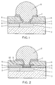
- Fig. 1 is a schematic diagram of a prior art C4 over Cu BEOL structure wherein a copper pad 1 is connected to a conductor 2 and within an opening or via through an isolation region 3.
- a barrier or liner layer (not shown) will be present on the sides and bottom of the copper pad, between the conductor 2 and isolation region 3.
- the isolation region 3 is typically silicon dioxide.
- the copper layer is typically about 0.3 to about 2 ⁇ m thick and more typically about 0.5 to about 1.2 ⁇ m thick.
- a capping layer 4 such as silicon nitride is provided above the copper layer.
- silicon nitride it can be deposited by a well known plasma enhanced chemical vapor deposition process (PECVD).
- PECVD plasma enhanced chemical vapor deposition process
- Such process involves introducing a silicon-bearing gas species such as silane and a nitrogen-bearing gas species such as ammonia and/or nitrogen in the presence of a plasma.
- silicon-bearing gas species include disilane, dichlorosilane and tetraethylorthosilicate.
- Other nitrogen-containing gas species include hexamethyldisilane.
- the deposition of the silicon nitride is usually carried out at temperatures of about 300 to about 450°C and more typically at temperatures of about 350 to about 400°C.
- the layer 4 is typically about 100 to about 20,000 ⁇ thick, more typically for silicon nitride the layer is about 100 to about 1000 ⁇ thick, and even more typically about 350 to about 700
- a via or opening is present in the capping layer 4 to provide access for subsequent interconnection to the C4 pad.
- a passivation layer 5 is provided on top of the capping layer 4.
- the passivation layer 5 also includes an opening or via to provide access for subsequent interconnection with a C4 pad.
- Passivation layer 5 is typically silicon dioxide, silicon nitride, silicon oxynitride or combinations thereof. In the case of silicon dioxide, the passivation layer 5 can be deposited by well-known techniques such as by plasma enhanced chemical vapor deposition.
- the preferred layer 5 is a combination of silicon dioxide layer followed by a silicon nitride layer. Typically, the thickness of layer 5 is about 1000 to about 9000 ⁇ .
- a dielectric layer 6 is provided above the passivation layer 5.
- the dielectric layer 6 also includes an opening or via to provide access for subsequent interconnection with a C4 pad.
- the preferred dielectric layer 6 is a polyimide.
- Polyimides suitable include unmodified polyimides, as well as modified polyimides, such as polyesterimides, polyimide-imide-esters, polyimide-imides, polysiloxaneimides, as well as other mixed polyimides. Such are well known in the prior art and need not be described herein in any great detail.
- the dielectric layer 6 is typically provided by coating with a polyimide precursor and then converting to the cured polyimide by heating. Commercially available polyimide precursors (polyamic acid) or various polyimide precursors from DuPont are available under the trade designation Pyralin.
- polyimide precursors come in many grades, including those available under the trade designations PI-2555, PI-2545, PI-2560, PI-5878, PIH-61454 and PI-2540. Some of these are pyromelletic dianhydride-oxydianiline (PMDA-ODA) polyimide precursors.
- PMDA-ODA pyromelletic dianhydride-oxydianiline
- the dielectric layer 6 is typically about 0.4 to about 5 microns thick and more typically about 10,000 to about 40,000 ⁇ thick.
- the pad-limiting metallurgy 7 located on top of copper 1 is the pad-limiting metallurgy 7.
- the layer 7 is also present on the sidewalls of the openings in capping layer 4, passivation layer 5 and dielectric layer 6.
- the pad-limiting metallurgy layer 7 is typically titanium nitride, copper, gold, titanium tungsten, chromium, which can be deposited as described in U.S. Patent 4,434,434 or U.S. Patent 5,629,564 , disclosures of which are incorporated herein by reference.
- a combination of layers are used in the pad limiting metallurgy, a particular combination being TiW followed by CrCu and then Cu.
- the TiW layer is typically about 250 to about 2000 ⁇ thick.
- the CrCu layer is typically 100 to about 2000 ⁇ thick.
- the Cu layer is typically about 1000 to 20,000 ⁇ thick.
- An in-situ sputter clean typically precedes the deposition of the first metal.
- a plated C4 pad or bump structure 8 connects directly to the pad limiting layer 7 through the openings or vias in the dielectric layer 6, passivation layer 5 and capping layer 4.
- the C4 contact bump structure 8 is mostly Pb-Sn solder and is provided on integrated circuit chips for making interconnections to substrates.
- the contact bump structure 8 is typically deposited on metal layer 7 for enhanced adhesion.
- the C4 bump extends above the integrated circuit chip by about 0.100 millimeters and is round or circular in cross-section parallel to the plane of the upper surface of the integrated circuit chip and is curved from its sides to the top surface of the bump where an interconnection is made to another electrode supported by a substrate.
- a layer 9 of AlCu and barrier 10 are provided between copper layer 1 and pad-limiting layer 7.
- the AlCu layer typically contains about 96 to about 99.5 atomic % Al, and correspondingly about 4 to about 0.5 atomic % Cu.
- the AlCu layer 9 is typically about 0.5 to about 1.2 microns. It can be applied by well known sputtering techniques.
- the barrier layer 10 is typically titanium, titanium nitride, tantalum or tantalum nitride, or mixtures, combinations or alloys thereof. In addition, often a combination of these barrier layers is employed, a particular combination being TaN followed by Ti and then TiN.
- the TaN layer is typically about 50 to about 1000 ⁇ thick.
- the Ti layer is 200 to 700 ⁇ thick.
- the TiN layer is 200 to 700 ⁇ thick.
- An in-situ sputter clean typically precedes the deposition of the first metal.
- the AlCu layer 9 and barrier layer 10 extends above and overlaps passivation layer 5. Moreover, preferably its width is substantially equal to the width of the copper layer 1.
- the dielectric layer 6 overlaps the overlap portion of the AlCu layer 9 and pad-limiting layer 7 overlaps portions of dielectric layer 6.
- the AlCu and barrier layers provide for a robust interconnection of the Co to the C4 pads.
- Tensile pull tests carried out demonstrated that the structures according to the present invention reduced the defect rate of 50-70% for prior art structures as shown in Fig. 1 to 0% for the structures of the present invention.
Landscapes
- Internal Circuitry In Semiconductor Integrated Circuit Devices (AREA)
- Wire Bonding (AREA)
- Parts Printed On Printed Circuit Boards (AREA)
- Exchange Systems With Centralized Control (AREA)
- Handling Of Sheets (AREA)
- Noodles (AREA)
- Non-Disconnectible Joints And Screw-Threaded Joints (AREA)
- Mechanical Coupling Of Light Guides (AREA)
- Connector Housings Or Holding Contact Members (AREA)
- Production Of Multi-Layered Print Wiring Board (AREA)
Abstract
Description
- The present invention relates to metal interconnects and more particularly to a robust copper interconnect structure. The present invention finds particular applicability for VLSI and ULSI copper interconnects especially for packaging.
- Interest in using copper as interconnects in semiconductor devices continues to increase since it possesses a lower resistivity and a reduced susceptibility to electromigration failure as compare to the more traditional aluminum or aluminum alloy interconnects.
- However, since copper has a tendency when used in interconnect metallurgy to diffuse into surrounding dielectric materials such as silicon dioxide, capping of the copper is essential. The capping inhibits this diffusion. One widely suggested method of capping includes employing a conductive barrier layer along the sidewalls and bottom surface of a copper interconnect. Typical of such barrier layers is tantalum or titanium. Capping of the upper surface of a copper interconnect usually employs silicon nitride.
- However, silicon nitride does not exhibit strong adhesion to copper surfaces despite various adhesion treatments. Accordingly, the silicon nitride-to-copper interface is susceptible to delamination under conditions of mechanical loading.
- For example, to assure package reliability, the C4 structural integrity must be sound in order to survive the mechanical stresses that the product experiences. Recent studies of C4 pads on copper interconnections reveal relatively weak C4 structural integrity. Failures arose during rework and burn-in operations due to the inherently relatively weak adhesion of the overlying silicon nitride cap to the copper.
-
US-A-5 898 222 describes capped copper electrical interconnects comprising a copper wiring layer which is capped with a material selected from a group including Ni and Al, the capping layer being said to provide improved adhesion and passivation. - According to one aspect of the invention there is provided a structure comprising layer of copper, a barrier layer, a layer of AlCu and a pad-limiting layer, wherein the layer of AlCu and barrier layer are interposed between the layer of copper and pad-limiting layer, and wherein the barrier layer is located between the layer of copper and the layer of AlCu.
- The present embodiment provides for improved structural integrity of copper interconnects including C4 over copper BEOL. The present invention provides for interconnect that is robust to mechanical stresses. The layer of copper may be about 3.0 to about 2 µm thick.
- More particularly, the structure of the present invention comprises a layer of copper, a pad limiting layer and a layer of AlCu and barrier interposed between the layer of copper and pad-limiting layer.
- The present embodiments also relates to an interconnect structure comprising a layer of copper, a capping layer located over the layer of copper and having a via to expose a portion of the layer of copper, a barrier layer located in the via and over the layer of copper, a layer of AlCu located over the barrier layer, and a pad-limiting layer located over the layer of AlCu.
- The barrier layer may overlap portions of the dielectric layer.
- The layer of copper may be about 0.3 to about 2 µm thick.
- The capping layer may comprise silicon nitride.
- The capping layer may be about 100 to about 1000 Å thick.
- The C4 contact bump may be Sn-Pb solder.
- The passivation layer may be selected from the group consisting of silicon dioxide, silicon nitride, silicon oxynitride and combinations thereof.
- The passivation layer is about 1000 to about 9000 Å thick.
- The dielectric may be a polyimide.
- The pad-limited layer may be selected from a least one member from a group consisting of titanium nitride, copper, gold, titanium tungsten, chromium and combinations thereof.
- The pad-limiting may comprise a TiW layer, followed by a CrCu layer, followed by a Cu layer.
- The pad-limiting layer may be selected from at least one member from the group consisting of titanium nitride, copper, gold, titanium tungsten, chromium and combinations thereof.
- The pad-limiting layer may comprise a TiW layer, followed by a CrCu layer, followed by a Cu layer
- Still other objects and advantages of the embodiment of the present invention will become readily apparent by those skilled in the art from the following detailed description, wherein it is shown and described only the preferred embodiments of the invention, simply by way of illustration of the best mode contemplated of carrying out the invention. As will be realized the invention is capable of other and different embodiments, and its several details are capable of modifications in various obvious respects, without departing from the invention. Accordingly, the description is to be regarded as illustrative in nature and not as restrictive.
-
-
Fig. 1 is a schematic diagram of a prior art C4 over Cu BEOL structure. -
Fig. 2 is a schematic diagram of a C4 over Cu BEOL structure according to the present invention. - In order to facilitate an understanding of the present invention, reference will be made to the drawings.
- In particular,
Fig. 1 is a schematic diagram of a prior art C4 over Cu BEOL structure wherein acopper pad 1 is connected to aconductor 2 and within an opening or via through anisolation region 3. Typically, a barrier or liner layer (not shown) will be present on the sides and bottom of the copper pad, between theconductor 2 andisolation region 3. - The
isolation region 3 is typically silicon dioxide. The copper layer is typically about 0.3 to about 2 µm thick and more typically about 0.5 to about 1.2 µm thick. - A
capping layer 4 such as silicon nitride is provided above the copper layer. In the case of silicon nitride, it can be deposited by a well known plasma enhanced chemical vapor deposition process (PECVD). Such process involves introducing a silicon-bearing gas species such as silane and a nitrogen-bearing gas species such as ammonia and/or nitrogen in the presence of a plasma. Other silicon-bearing gas species include disilane, dichlorosilane and tetraethylorthosilicate. Other nitrogen-containing gas species include hexamethyldisilane. The deposition of the silicon nitride is usually carried out at temperatures of about 300 to about 450°C and more typically at temperatures of about 350 to about 400°C. Thelayer 4 is typically about 100 to about 20,000 Å thick, more typically for silicon nitride the layer is about 100 to about 1000 Å thick, and even more typically about 350 to about 700 Å thick for silicon nitride. - A via or opening is present in the
capping layer 4 to provide access for subsequent interconnection to the C4 pad. - A
passivation layer 5 is provided on top of thecapping layer 4. Thepassivation layer 5 also includes an opening or via to provide access for subsequent interconnection with a C4 pad.Passivation layer 5 is typically silicon dioxide, silicon nitride, silicon oxynitride or combinations thereof. In the case of silicon dioxide, thepassivation layer 5 can be deposited by well-known techniques such as by plasma enhanced chemical vapor deposition. Thepreferred layer 5 is a combination of silicon dioxide layer followed by a silicon nitride layer. Typically, the thickness oflayer 5 is about 1000 to about 9000 Å. - A
dielectric layer 6 is provided above thepassivation layer 5. Thedielectric layer 6 also includes an opening or via to provide access for subsequent interconnection with a C4 pad. - The preferred
dielectric layer 6 is a polyimide. Polyimides suitable include unmodified polyimides, as well as modified polyimides, such as polyesterimides, polyimide-imide-esters, polyimide-imides, polysiloxaneimides, as well as other mixed polyimides. Such are well known in the prior art and need not be described herein in any great detail. Thedielectric layer 6 is typically provided by coating with a polyimide precursor and then converting to the cured polyimide by heating. Commercially available polyimide precursors (polyamic acid) or various polyimide precursors from DuPont are available under the trade designation Pyralin. These polyimide precursors come in many grades, including those available under the trade designations PI-2555, PI-2545, PI-2560, PI-5878, PIH-61454 and PI-2540. Some of these are pyromelletic dianhydride-oxydianiline (PMDA-ODA) polyimide precursors. - The
dielectric layer 6 is typically about 0.4 to about 5 microns thick and more typically about 10,000 to about 40,000 Å thick. - In the art as currently practiced, located on top of
copper 1 is the pad-limitingmetallurgy 7. Thelayer 7 is also present on the sidewalls of the openings in cappinglayer 4,passivation layer 5 anddielectric layer 6. - The pad-limiting
metallurgy layer 7 is typically titanium nitride, copper, gold, titanium tungsten, chromium, which can be deposited as described inU.S. Patent 4,434,434 orU.S. Patent 5,629,564 , disclosures of which are incorporated herein by reference. Typically, a combination of layers are used in the pad limiting metallurgy, a particular combination being TiW followed by CrCu and then Cu. The TiW layer is typically about 250 to about 2000 Å thick. The CrCu layer is typically 100 to about 2000 Å thick. The Cu layer is typically about 1000 to 20,000 Å thick. An in-situ sputter clean typically precedes the deposition of the first metal. - A plated C4 pad or bump
structure 8 connects directly to thepad limiting layer 7 through the openings or vias in thedielectric layer 6,passivation layer 5 andcapping layer 4. - The C4
contact bump structure 8 is mostly Pb-Sn solder and is provided on integrated circuit chips for making interconnections to substrates. Thecontact bump structure 8 is typically deposited onmetal layer 7 for enhanced adhesion. The C4 bump extends above the integrated circuit chip by about 0.100 millimeters and is round or circular in cross-section parallel to the plane of the upper surface of the integrated circuit chip and is curved from its sides to the top surface of the bump where an interconnection is made to another electrode supported by a substrate. - During chip pull rework or post-burn-in, a normal or shear force is exerted on the
cap 4 overlying thecopper 1. Due to poor adhesion, the cap can crack and delaminate from the copper surface. This failure mode renders the Cu interconnect technology less reliable for multichip module applications and some single chip uses. - Pursuant to the present invention, as illustrated in
Fig. 2 , alayer 9 of AlCu andbarrier 10 are provided betweencopper layer 1 and pad-limitinglayer 7. The AlCu layer typically contains about 96 to about 99.5 atomic % Al, and correspondingly about 4 to about 0.5 atomic % Cu. TheAlCu layer 9 is typically about 0.5 to about 1.2 microns. It can be applied by well known sputtering techniques. - The
barrier layer 10 is typically titanium, titanium nitride, tantalum or tantalum nitride, or mixtures, combinations or alloys thereof. In addition, often a combination of these barrier layers is employed, a particular combination being TaN followed by Ti and then TiN. The TaN layer is typically about 50 to about 1000 Å thick. The Ti layer is 200 to 700 Å thick. The TiN layer is 200 to 700 Å thick. An in-situ sputter clean typically precedes the deposition of the first metal. - According to preferred aspects of the present invention, the
AlCu layer 9 andbarrier layer 10 extends above and overlapspassivation layer 5. Moreover, preferably its width is substantially equal to the width of thecopper layer 1. - Moreover, in a preferred configuration, the
dielectric layer 6 overlaps the overlap portion of theAlCu layer 9 and pad-limitinglayer 7 overlaps portions ofdielectric layer 6. - The AlCu and barrier layers provide for a robust interconnection of the Co to the C4 pads. Tensile pull tests carried out demonstrated that the structures according to the present invention reduced the defect rate of 50-70% for prior art structures as shown in
Fig. 1 to 0% for the structures of the present invention. - The foregoing description of the invention illustrates and describes the present invention. Additionally, the disclosure shows and describes only the preferred embodiments of the invention but, as mentioned above, it is to be understood that the invention is capable of use in various other combinations, modifications, and environments and is capable of changes or modifications within the scope of the inventive concept as expressed herein, commensurate with the above teachings and/or the skill or knowledge of the relevant art. The embodiments described hereinabove are further intended to explain best modes known of practicing the invention and to enable others skilled in the art to utilize the invention in such, or other, embodiments and with the various modifications required by the particular applications or uses of the invention. Accordingly, the description is not intended to limit the invention to the form disclosed herein.
Claims (12)
- An interconnect structure comprising layer of copper, a barrier layer, a layer of AlCu and a pad-limiting layer, wherein the layer of AlCu and barrier layer are interposed between the layer of copper and pad-limiting layer, and wherein the barrier layer is located between the layer of copper and the layer of AlCu.
- The interconnect structure of claim 1 further comprising a capping layer located over the layer of copper and having a via to expose a portion of the layer of copper, whereby the barrier layer is located in the via and over the layer of copper, and the layer of AlCu is located in the via and over the barrier layer, and the pad limiting layer is located over the layer of AlCu.
- The interconnect structure of claim 2 which further comprises C4 contact bump in contact with the pad limiting layer.
- The interconnect structure of claim 2 or 3 which further comprises a passivation layer located over the capping layer and having a via that coincides with the via in the capping layer and optionally one or more of the following:a portion of the layer of AlCu extends above and overlaps the passivation layer; and/orthe layer of the barrier layer extends above and overlaps the passivation layer.
- The interconnect structure of any of claims 2 to 4 wherein the layer of AlCu has a width that is substantially equal to the width of the layer of copper and/or in the barrier layer has a width that is substantially equal to the width of the layer of copper.
- The interconnect structure of claim 4 which further comprises a dielectric layer located above the passivation layer, optionally the dielectric layer overlaps the overlapping portion of the layer of AlCu.
- The interconnect structure of claim 6 wherein the pad limiting layer overlaps the dielectric layer.
- The structure of any of claims 1 to 7 further comprising one or more of the following:the layer of copper is about 0.3 to about 2 µm thick;the layer of AlCu contains about 96 to about 99.5 atomic % of Al;the layer of AlCu is about 0.5 to about 1.2 microns thick;the barrier layer is selected from the group consisting of titanium, tantalum, nitrides thereof, mixtures thereof, combinations thereof and alloys thereof;the barrier layer is about 50 to about 1000 Å thick;the barrier layer is a combination of a TaN layer, a Ti layer and a TiN layer;the TiN layer is about 200 to about 700 Å thick, the Ti layer is about 200 to about 700 Å thick, and the TaN layer is about 50 to about 1000 Å thick;the capping layer comprises silicon nitride; and/orthe capping layer is about 100 to about 1000 Å thick.
- The interconnect structure of claim 3 or any of the preceding claims where dependent on claim 3 wherein the C4 contact bump is Sn-Pb solder.
- The interconnect structure of claim 4 or any of the preceding claims where dependent on claim 4 wherein the passivation layer is selected from the group consisting of silicon dioxide, silicon nitride, silicon oxynitride and combinations thereof, optionally the passivation layer is about 1000 to about 9000 Å thick.
- The interconnect structure of claim 6 or any of the preceding claims where dependent on claim 6 wherein the dielectric layer is a polyimide.
- The structure of any of claims 1 to 11 wherein the pad-limiting layer is selected from at least one member from the group consisting of titanium nitride, copper, gold, titanium tungsten, chromium and combinations thereof, optionally the pad-limiting layer comprises a TiW layer, followed by a CrCu layer, followed by a Cu layer.
Applications Claiming Priority (3)
| Application Number | Priority Date | Filing Date | Title |
|---|---|---|---|
| US09/314,003 US6133136A (en) | 1999-05-19 | 1999-05-19 | Robust interconnect structure |
| US314003 | 1999-05-19 | ||
| PCT/GB2000/001847 WO2000072380A1 (en) | 1999-05-19 | 2000-05-15 | Robust interconnect structure |
Publications (2)
| Publication Number | Publication Date |
|---|---|
| EP1186034A1 EP1186034A1 (en) | 2002-03-13 |
| EP1186034B1 true EP1186034B1 (en) | 2009-03-18 |
Family
ID=23218114
Family Applications (1)
| Application Number | Title | Priority Date | Filing Date |
|---|---|---|---|
| EP00931376A Expired - Lifetime EP1186034B1 (en) | 1999-05-19 | 2000-05-15 | Robust interconnect structure |
Country Status (17)
| Country | Link |
|---|---|
| US (1) | US6133136A (en) |
| EP (1) | EP1186034B1 (en) |
| JP (1) | JP3898894B2 (en) |
| KR (1) | KR100463492B1 (en) |
| CN (1) | CN1165081C (en) |
| AT (1) | ATE426247T1 (en) |
| AU (1) | AU4933500A (en) |
| CA (1) | CA2368950C (en) |
| CZ (1) | CZ302748B6 (en) |
| DE (1) | DE60041817D1 (en) |
| ES (1) | ES2320523T3 (en) |
| HU (1) | HUP0201473A2 (en) |
| IL (1) | IL146333A (en) |
| MY (1) | MY118419A (en) |
| PL (1) | PL201072B1 (en) |
| TW (1) | TW473921B (en) |
| WO (1) | WO2000072380A1 (en) |
Cited By (1)
| Publication number | Priority date | Publication date | Assignee | Title |
|---|---|---|---|---|
| DE112017001420B4 (en) | 2016-06-30 | 2022-09-01 | International Business Machines Corporation | Techniques for Improving Reliability in Cu Interconnects Using Cu Intermetallics |
Families Citing this family (39)
| Publication number | Priority date | Publication date | Assignee | Title |
|---|---|---|---|---|
| US6187680B1 (en) * | 1998-10-07 | 2001-02-13 | International Business Machines Corporation | Method/structure for creating aluminum wirebound pad on copper BEOL |
| JP3387083B2 (en) * | 1999-08-27 | 2003-03-17 | 日本電気株式会社 | Semiconductor device and manufacturing method thereof |
| US6451681B1 (en) * | 1999-10-04 | 2002-09-17 | Motorola, Inc. | Method of forming copper interconnection utilizing aluminum capping film |
| US6191023B1 (en) * | 1999-11-18 | 2001-02-20 | Taiwan Semiconductor Manufacturing Company | Method of improving copper pad adhesion |
| US6387793B1 (en) | 2000-03-09 | 2002-05-14 | Hrl Laboratories, Llc | Method for manufacturing precision electroplated solder bumps |
| JP3651765B2 (en) * | 2000-03-27 | 2005-05-25 | 株式会社東芝 | Semiconductor device |
| US6551931B1 (en) * | 2000-11-07 | 2003-04-22 | International Business Machines Corporation | Method to selectively cap interconnects with indium or tin bronzes and/or oxides thereof and the interconnect so capped |
| US20030116845A1 (en) * | 2001-12-21 | 2003-06-26 | Bojkov Christo P. | Waferlevel method for direct bumping on copper pads in integrated circuits |
| JP3759909B2 (en) * | 2002-02-22 | 2006-03-29 | 松下電器産業株式会社 | Semiconductor device and manufacturing method thereof |
| US20030227091A1 (en) * | 2002-06-06 | 2003-12-11 | Nishant Sinha | Plating metal caps on conductive interconnect for wirebonding |
| US6875693B1 (en) * | 2003-03-26 | 2005-04-05 | Lsi Logic Corporation | Via and metal line interface capable of reducing the incidence of electro-migration induced voids |
| US6835580B1 (en) * | 2003-06-26 | 2004-12-28 | Semiconductor Components Industries, L.L.C. | Direct chip attach structure and method |
| US6951775B2 (en) * | 2003-06-28 | 2005-10-04 | International Business Machines Corporation | Method for forming interconnects on thin wafers |
| US20050098605A1 (en) * | 2003-11-06 | 2005-05-12 | International Business Machines Corporation | Apparatus and method for low pressure wirebond |
| US7068138B2 (en) * | 2004-01-29 | 2006-06-27 | International Business Machines Corporation | High Q factor integrated circuit inductor |
| KR100605315B1 (en) | 2004-07-30 | 2006-07-28 | 삼성전자주식회사 | Input / Output Pad Structure of Integrated Circuit Chip |
| JP2006120677A (en) * | 2004-10-19 | 2006-05-11 | Alps Electric Co Ltd | Connection terminal structure of wiring board |
| US7282433B2 (en) * | 2005-01-10 | 2007-10-16 | Micron Technology, Inc. | Interconnect structures with bond-pads and methods of forming bump sites on bond-pads |
| US20100117231A1 (en) * | 2006-08-30 | 2010-05-13 | Dennis Lang | Reliable wafer-level chip-scale solder bump structure |
| JP2008159948A (en) * | 2006-12-25 | 2008-07-10 | Rohm Co Ltd | Semiconductor device |
| US20080157382A1 (en) * | 2006-12-28 | 2008-07-03 | Chinthakindi Anil K | Direct termination of a wiring metal in a semiconductor device |
| US7935408B2 (en) * | 2007-10-26 | 2011-05-03 | International Business Machines Corporation | Substrate anchor structure and method |
| JP5627835B2 (en) | 2007-11-16 | 2014-11-19 | ローム株式会社 | Semiconductor device and manufacturing method of semiconductor device |
| US7868453B2 (en) * | 2008-02-15 | 2011-01-11 | International Business Machines Corporation | Solder interconnect pads with current spreading layers |
| CN101630667A (en) * | 2008-07-15 | 2010-01-20 | 中芯国际集成电路制造(上海)有限公司 | Method and system for forming conductive bump with copper interconnections |
| US7851346B2 (en) * | 2008-07-21 | 2010-12-14 | Taiwan Semiconductor Manufacturing Company, Ltd. | Bonding metallurgy for three-dimensional interconnect |
| JP5249080B2 (en) * | 2009-02-19 | 2013-07-31 | セイコーインスツル株式会社 | Semiconductor device |
| JP5316261B2 (en) * | 2009-06-30 | 2013-10-16 | 富士通株式会社 | Multichip module, printed circuit board unit and electronic device |
| US8610283B2 (en) | 2009-10-05 | 2013-12-17 | International Business Machines Corporation | Semiconductor device having a copper plug |
| US9214385B2 (en) | 2009-12-17 | 2015-12-15 | Globalfoundries Inc. | Semiconductor device including passivation layer encapsulant |
| US8446006B2 (en) * | 2009-12-17 | 2013-05-21 | International Business Machines Corporation | Structures and methods to reduce maximum current density in a solder ball |
| US8492892B2 (en) | 2010-12-08 | 2013-07-23 | International Business Machines Corporation | Solder bump connections |
| US20120326299A1 (en) * | 2011-06-24 | 2012-12-27 | Topacio Roden R | Semiconductor chip with dual polymer film interconnect structures |
| CN104051323B (en) * | 2013-03-13 | 2017-12-29 | 中芯国际集成电路制造(上海)有限公司 | A kind of semiconductor package and preparation method thereof |
| CN104241146B (en) * | 2013-06-09 | 2017-10-31 | 中芯国际集成电路制造(上海)有限公司 | The forming method and semiconductor structure of metal gasket |
| US10002834B2 (en) * | 2015-03-11 | 2018-06-19 | Applied Materials, Inc. | Method and apparatus for protecting metal interconnect from halogen based precursors |
| CN106505031B (en) * | 2015-09-07 | 2019-12-31 | 中芯国际集成电路制造(上海)有限公司 | Manufacturing method of copper interconnection structure, copper interconnection structure and electronic device |
| US10535698B2 (en) | 2017-11-28 | 2020-01-14 | Taiwan Semiconductor Manufacturing Co., Ltd. | Image sensor with pad structure |
| JP7430481B2 (en) * | 2018-05-31 | 2024-02-13 | 新光電気工業株式会社 | Wiring board, semiconductor device, and wiring board manufacturing method |
Family Cites Families (9)
| Publication number | Priority date | Publication date | Assignee | Title |
|---|---|---|---|---|
| US4434434A (en) * | 1981-03-30 | 1984-02-28 | International Business Machines Corporation | Solder mound formation on substrates |
| US5268072A (en) * | 1992-08-31 | 1993-12-07 | International Business Machines Corporation | Etching processes for avoiding edge stress in semiconductor chip solder bumps |
| US5503286A (en) * | 1994-06-28 | 1996-04-02 | International Business Machines Corporation | Electroplated solder terminal |
| US5545927A (en) * | 1995-05-12 | 1996-08-13 | International Business Machines Corporation | Capped copper electrical interconnects |
| EP0751566A3 (en) * | 1995-06-30 | 1997-02-26 | Ibm | Barrier layer comprising a thin metallic film for electrical interconnections |
| US5785236A (en) * | 1995-11-29 | 1998-07-28 | Advanced Micro Devices, Inc. | Advanced copper interconnect system that is compatible with existing IC wire bonding technology |
| US5731624A (en) * | 1996-06-28 | 1998-03-24 | International Business Machines Corporation | Integrated pad and fuse structure for planar copper metallurgy |
| US6020640A (en) * | 1996-12-19 | 2000-02-01 | Texas Instruments Incorporated | Thick plated interconnect and associated auxillary interconnect |
| JPH11340265A (en) * | 1998-05-22 | 1999-12-10 | Sony Corp | Semiconductor device and manufacturing method thereof |
-
1999
- 1999-05-19 US US09/314,003 patent/US6133136A/en not_active Expired - Lifetime
-
2000
- 2000-05-08 MY MYPI20001978A patent/MY118419A/en unknown
- 2000-05-15 CN CNB008074356A patent/CN1165081C/en not_active Expired - Lifetime
- 2000-05-15 WO PCT/GB2000/001847 patent/WO2000072380A1/en not_active Ceased
- 2000-05-15 AT AT00931376T patent/ATE426247T1/en not_active IP Right Cessation
- 2000-05-15 AU AU49335/00A patent/AU4933500A/en not_active Abandoned
- 2000-05-15 CZ CZ20014145A patent/CZ302748B6/en not_active IP Right Cessation
- 2000-05-15 HU HU0201473A patent/HUP0201473A2/en unknown
- 2000-05-15 ES ES00931376T patent/ES2320523T3/en not_active Expired - Lifetime
- 2000-05-15 EP EP00931376A patent/EP1186034B1/en not_active Expired - Lifetime
- 2000-05-15 KR KR10-2001-7014357A patent/KR100463492B1/en not_active Expired - Lifetime
- 2000-05-15 DE DE60041817T patent/DE60041817D1/en not_active Expired - Lifetime
- 2000-05-15 JP JP2000620678A patent/JP3898894B2/en not_active Expired - Lifetime
- 2000-05-15 PL PL351305A patent/PL201072B1/en not_active IP Right Cessation
- 2000-05-15 CA CA2368950A patent/CA2368950C/en not_active Expired - Fee Related
- 2000-05-15 IL IL14633300A patent/IL146333A/en not_active IP Right Cessation
- 2000-05-16 TW TW089109347A patent/TW473921B/en not_active IP Right Cessation
Cited By (1)
| Publication number | Priority date | Publication date | Assignee | Title |
|---|---|---|---|---|
| DE112017001420B4 (en) | 2016-06-30 | 2022-09-01 | International Business Machines Corporation | Techniques for Improving Reliability in Cu Interconnects Using Cu Intermetallics |
Also Published As
| Publication number | Publication date |
|---|---|
| DE60041817D1 (en) | 2009-04-30 |
| IL146333A (en) | 2005-03-20 |
| HUP0201473A2 (en) | 2002-08-28 |
| CN1350703A (en) | 2002-05-22 |
| ATE426247T1 (en) | 2009-04-15 |
| ES2320523T3 (en) | 2009-05-25 |
| KR20020005743A (en) | 2002-01-17 |
| AU4933500A (en) | 2000-12-12 |
| CZ20014145A3 (en) | 2002-04-17 |
| CN1165081C (en) | 2004-09-01 |
| CA2368950A1 (en) | 2000-11-30 |
| KR100463492B1 (en) | 2004-12-29 |
| JP2003500860A (en) | 2003-01-07 |
| TW473921B (en) | 2002-01-21 |
| IL146333A0 (en) | 2002-07-25 |
| MY118419A (en) | 2004-10-30 |
| EP1186034A1 (en) | 2002-03-13 |
| CZ302748B6 (en) | 2011-10-19 |
| PL201072B1 (en) | 2009-03-31 |
| JP3898894B2 (en) | 2007-03-28 |
| PL351305A1 (en) | 2003-04-07 |
| US6133136A (en) | 2000-10-17 |
| CA2368950C (en) | 2012-10-02 |
| WO2000072380A1 (en) | 2000-11-30 |
Similar Documents
| Publication | Publication Date | Title |
|---|---|---|
| US6133136A (en) | Robust interconnect structure | |
| US6489229B1 (en) | Method of forming a semiconductor device having conductive bumps without using gold | |
| US6451681B1 (en) | Method of forming copper interconnection utilizing aluminum capping film | |
| US6534863B2 (en) | Common ball-limiting metallurgy for I/O sites | |
| US7741714B2 (en) | Bond pad structure with stress-buffering layer capping interconnection metal layer | |
| US7271030B2 (en) | Direct bumping on integrated circuit contacts enabled by metal-to-insulator adhesion | |
| US8119456B2 (en) | Bond pad for wafer and package for CMOS imager | |
| US20080122078A1 (en) | Systems and methods to passivate on-die redistribution interconnects | |
| US5070036A (en) | Process for contacting and interconnecting semiconductor devices within an integrated circuit | |
| US6806578B2 (en) | Copper pad structure | |
| US20100213608A1 (en) | Solder bump UBM structure | |
| US20030020163A1 (en) | Bonding pad structure for copper/low-k dielectric material BEOL process | |
| CN102088004A (en) | Integrated circuit element and flip chip package | |
| US4977440A (en) | Structure and process for contacting and interconnecting semiconductor devices within an integrated circuit | |
| US20110018128A1 (en) | Package structure and method for reducing dielectric layer delamination | |
| US6312830B1 (en) | Method and an apparatus for forming an under bump metallization structure | |
| US20050098605A1 (en) | Apparatus and method for low pressure wirebond | |
| US20070222073A1 (en) | Structure and method to improve current-carrying capabilities of c4 joints | |
| US6462417B1 (en) | Coherent alloy diffusion barrier for integrated circuit interconnects | |
| US6445070B1 (en) | Coherent carbide diffusion barrier for integrated circuit interconnects | |
| US20100283146A1 (en) | Semiconductor structure and method of fabricating the same | |
| JP2723023B2 (en) | Semiconductor device and manufacturing method thereof | |
| JP3726529B2 (en) | Semiconductor device |
Legal Events
| Date | Code | Title | Description |
|---|---|---|---|
| PUAI | Public reference made under article 153(3) epc to a published international application that has entered the european phase |
Free format text: ORIGINAL CODE: 0009012 |
|
| 17P | Request for examination filed |
Effective date: 20011203 |
|
| AK | Designated contracting states |
Kind code of ref document: A1 Designated state(s): AT BE CH CY DE DK ES FI FR GB GR IE IT LI LU MC NL PT SE |
|
| AX | Request for extension of the european patent |
Free format text: AL;LT;LV;MK;RO;SI |
|
| GRAP | Despatch of communication of intention to grant a patent |
Free format text: ORIGINAL CODE: EPIDOSNIGR1 |
|
| GRAS | Grant fee paid |
Free format text: ORIGINAL CODE: EPIDOSNIGR3 |
|
| GRAA | (expected) grant |
Free format text: ORIGINAL CODE: 0009210 |
|
| GRAL | Information related to payment of fee for publishing/printing deleted |
Free format text: ORIGINAL CODE: EPIDOSDIGR3 |
|
| GRAS | Grant fee paid |
Free format text: ORIGINAL CODE: EPIDOSNIGR3 |
|
| RAP1 | Party data changed (applicant data changed or rights of an application transferred) |
Owner name: IBM UNITED KINGDOM LIMITED Owner name: INTERNATIONAL BUSINESS MACHINES CORPORATION |
|
| RBV | Designated contracting states (corrected) |
Designated state(s): AT BE CH CY DE DK ES FI FR GB GR IE IT LI LU NL PT SE |
|
| RAP1 | Party data changed (applicant data changed or rights of an application transferred) |
Owner name: INTERNATIONAL BUSINESS MACHINES CORPORATION |
|
| AK | Designated contracting states |
Kind code of ref document: B1 Designated state(s): AT BE CH CY DE DK ES FI FR GB GR IE IT LI LU NL PT SE |
|
| REG | Reference to a national code |
Ref country code: GB Ref legal event code: FG4D |
|
| REG | Reference to a national code |
Ref country code: CH Ref legal event code: EP |
|
| REG | Reference to a national code |
Ref country code: IE Ref legal event code: FG4D |
|
| REF | Corresponds to: |
Ref document number: 60041817 Country of ref document: DE Date of ref document: 20090430 Kind code of ref document: P |
|
| REG | Reference to a national code |
Ref country code: GB Ref legal event code: 746 Effective date: 20090417 |
|
| REG | Reference to a national code |
Ref country code: ES Ref legal event code: FG2A Ref document number: 2320523 Country of ref document: ES Kind code of ref document: T3 |
|
| REG | Reference to a national code |
Ref country code: CH Ref legal event code: NV Representative=s name: IBM RESEARCH GMBH ZURICH RESEARCH LABORATORY INTEL |
|
| REG | Reference to a national code |
Ref country code: SE Ref legal event code: TRGR |
|
| PG25 | Lapsed in a contracting state [announced via postgrant information from national office to epo] |
Ref country code: FI Free format text: LAPSE BECAUSE OF FAILURE TO SUBMIT A TRANSLATION OF THE DESCRIPTION OR TO PAY THE FEE WITHIN THE PRESCRIBED TIME-LIMIT Effective date: 20090318 |
|
| PG25 | Lapsed in a contracting state [announced via postgrant information from national office to epo] |
Ref country code: AT Free format text: LAPSE BECAUSE OF FAILURE TO SUBMIT A TRANSLATION OF THE DESCRIPTION OR TO PAY THE FEE WITHIN THE PRESCRIBED TIME-LIMIT Effective date: 20090318 |
|
| REG | Reference to a national code |
Ref country code: CH Ref legal event code: PUE Owner name: TESSERA INTELLECTUAL PROPERTIES, INC. Free format text: INTERNATIONAL BUSINESS MACHINES CORPORATION#NEW ORCHARD ROAD#ARMONK, NY 10504 (US) -TRANSFER TO- TESSERA INTELLECTUAL PROPERTIES, INC.#3025 ORCHARD PARKWAY#SAN JOSE, CA 95134 (US) Ref country code: CH Ref legal event code: NV Representative=s name: ISLER & PEDRAZZINI AG |
|
| REG | Reference to a national code |
Ref country code: GB Ref legal event code: 732E Free format text: REGISTERED BETWEEN 20090813 AND 20090819 |
|
| PG25 | Lapsed in a contracting state [announced via postgrant information from national office to epo] |
Ref country code: BE Free format text: LAPSE BECAUSE OF FAILURE TO SUBMIT A TRANSLATION OF THE DESCRIPTION OR TO PAY THE FEE WITHIN THE PRESCRIBED TIME-LIMIT Effective date: 20090318 |
|
| PG25 | Lapsed in a contracting state [announced via postgrant information from national office to epo] |
Ref country code: PT Free format text: LAPSE BECAUSE OF FAILURE TO SUBMIT A TRANSLATION OF THE DESCRIPTION OR TO PAY THE FEE WITHIN THE PRESCRIBED TIME-LIMIT Effective date: 20090826 |
|
| NLS | Nl: assignments of ep-patents |
Owner name: TESSERA INTELLECTUAL PROPERTIES, INC. Effective date: 20090828 |
|
| RAP2 | Party data changed (patent owner data changed or rights of a patent transferred) |
Owner name: TESSERA INTELLECTUAL PROPERTIES, INC. |
|
| REG | Reference to a national code |
Ref country code: FR Ref legal event code: TP |
|
| PLBE | No opposition filed within time limit |
Free format text: ORIGINAL CODE: 0009261 |
|
| STAA | Information on the status of an ep patent application or granted ep patent |
Free format text: STATUS: NO OPPOSITION FILED WITHIN TIME LIMIT |
|
| PG25 | Lapsed in a contracting state [announced via postgrant information from national office to epo] |
Ref country code: DK Free format text: LAPSE BECAUSE OF FAILURE TO SUBMIT A TRANSLATION OF THE DESCRIPTION OR TO PAY THE FEE WITHIN THE PRESCRIBED TIME-LIMIT Effective date: 20090318 |
|
| NLT2 | Nl: modifications (of names), taken from the european patent patent bulletin |
Owner name: TESSERA INTELLECTUAL PROPERTIES, INC. Effective date: 20091118 |
|
| 26N | No opposition filed |
Effective date: 20091221 |
|
| PG25 | Lapsed in a contracting state [announced via postgrant information from national office to epo] |
Ref country code: GR Free format text: LAPSE BECAUSE OF FAILURE TO SUBMIT A TRANSLATION OF THE DESCRIPTION OR TO PAY THE FEE WITHIN THE PRESCRIBED TIME-LIMIT Effective date: 20090619 |
|
| PG25 | Lapsed in a contracting state [announced via postgrant information from national office to epo] |
Ref country code: LU Free format text: LAPSE BECAUSE OF NON-PAYMENT OF DUE FEES Effective date: 20090515 |
|
| PG25 | Lapsed in a contracting state [announced via postgrant information from national office to epo] |
Ref country code: CY Free format text: LAPSE BECAUSE OF FAILURE TO SUBMIT A TRANSLATION OF THE DESCRIPTION OR TO PAY THE FEE WITHIN THE PRESCRIBED TIME-LIMIT Effective date: 20090318 |
|
| REG | Reference to a national code |
Ref country code: CH Ref legal event code: PFA Owner name: INVENSAS CORPORATION Free format text: TESSERA INTELLECTUAL PROPERTIES, INC.#3025 ORCHARD PARKWAY#SAN JOSE, CA 95134 (US) -TRANSFER TO- INVENSAS CORPORATION#3025 ORCHARD PARKWAY#SAN JOSE, CA 95134 (US) |
|
| REG | Reference to a national code |
Ref country code: DE Ref legal event code: R082 Ref document number: 60041817 Country of ref document: DE Representative=s name: SCHWABE, SANDMAIR, MARX, DE |
|
| REG | Reference to a national code |
Ref country code: NL Ref legal event code: TD Effective date: 20111013 |
|
| REG | Reference to a national code |
Ref country code: DE Ref legal event code: R081 Ref document number: 60041817 Country of ref document: DE Owner name: INVENSAS CORP., (N. D. GES. D. STAATES DELAWAR, US Free format text: FORMER OWNER: TESSERA INTELLECTUAL PROPERTIES, INC., (N. D. GES. D. STAATES DELAWARE), SAN JOSE, US Effective date: 20111019 Ref country code: DE Ref legal event code: R082 Ref document number: 60041817 Country of ref document: DE Representative=s name: SCHWABE SANDMAIR MARX, DE Effective date: 20111019 Ref country code: DE Ref legal event code: R081 Ref document number: 60041817 Country of ref document: DE Owner name: INVENSAS CORP., (N. D. GES. D. STAATES DELAWAR, US Free format text: FORMER OWNER: TESSERA INTELLECTUAL PROPERTIES, INC., (N. D. GES. D. STAATES DELAWARE), SAN JOSE, CALIF., US Effective date: 20111019 Ref country code: DE Ref legal event code: R082 Ref document number: 60041817 Country of ref document: DE Representative=s name: SCHWABE SANDMAIR MARX PATENTANWAELTE RECHTSANW, DE Effective date: 20111019 |
|
| REG | Reference to a national code |
Ref country code: FR Ref legal event code: CD Owner name: INVENSAS CORPORATION, US Effective date: 20111123 |
|
| REG | Reference to a national code |
Ref country code: CH Ref legal event code: PFA Owner name: INVENSAS CORPORATION Free format text: INVENSAS CORPORATION#3025 ORCHARD PARKWAY#SAN JOSE, CA 95134 (US) -TRANSFER TO- INVENSAS CORPORATION#2702 ORCHARD PARKWAY#SAN JOSE, CA 95134 (US) |
|
| REG | Reference to a national code |
Ref country code: ES Ref legal event code: PC2A Owner name: INVENSAS CORPORATION Effective date: 20120207 |
|
| REG | Reference to a national code |
Ref country code: FR Ref legal event code: CA Effective date: 20120724 |
|
| PGFP | Annual fee paid to national office [announced via postgrant information from national office to epo] |
Ref country code: CH Payment date: 20130426 Year of fee payment: 14 Ref country code: SE Payment date: 20130507 Year of fee payment: 14 Ref country code: IE Payment date: 20130510 Year of fee payment: 14 |
|
| PGFP | Annual fee paid to national office [announced via postgrant information from national office to epo] |
Ref country code: IT Payment date: 20130521 Year of fee payment: 14 |
|
| REG | Reference to a national code |
Ref country code: CH Ref legal event code: PL |
|
| PG25 | Lapsed in a contracting state [announced via postgrant information from national office to epo] |
Ref country code: SE Free format text: LAPSE BECAUSE OF NON-PAYMENT OF DUE FEES Effective date: 20140516 Ref country code: LI Free format text: LAPSE BECAUSE OF NON-PAYMENT OF DUE FEES Effective date: 20140531 Ref country code: CH Free format text: LAPSE BECAUSE OF NON-PAYMENT OF DUE FEES Effective date: 20140531 |
|
| REG | Reference to a national code |
Ref country code: SE Ref legal event code: EUG |
|
| REG | Reference to a national code |
Ref country code: IE Ref legal event code: MM4A |
|
| PG25 | Lapsed in a contracting state [announced via postgrant information from national office to epo] |
Ref country code: IE Free format text: LAPSE BECAUSE OF NON-PAYMENT OF DUE FEES Effective date: 20140515 Ref country code: IT Free format text: LAPSE BECAUSE OF NON-PAYMENT OF DUE FEES Effective date: 20140515 |
|
| REG | Reference to a national code |
Ref country code: FR Ref legal event code: PLFP Year of fee payment: 16 |
|
| REG | Reference to a national code |
Ref country code: DE Ref legal event code: R085 Ref document number: 60041817 Country of ref document: DE |
|
| REG | Reference to a national code |
Ref country code: FR Ref legal event code: PLFP Year of fee payment: 17 |
|
| REG | Reference to a national code |
Ref country code: GB Ref legal event code: S47 Free format text: CANCELLATION OF ENTRY; APPLICATION FOR CANCELLATION OF ENTRY ON THE REGISTER OF A LICENCE OF RIGHT FILED ON 11 JULY 2016 |
|
| REG | Reference to a national code |
Ref country code: DE Ref legal event code: R008 Ref document number: 60041817 Country of ref document: DE Ref country code: DE Ref legal event code: R039 Ref document number: 60041817 Country of ref document: DE |
|
| REG | Reference to a national code |
Ref country code: GB Ref legal event code: S47 Free format text: ENTRY CANCELLED; NOTICE IS HEREBY GIVEN THAT THE LICENCE OF RIGHT ENTRY ON THE REGISTER FOR THE FOLLOWING PATENT WAS CANCELLED ON 8 NOVEMBER 2016. INVENSAS CORPORATION ROBUST INTERCONNECT STRUCTURE |
|
| REG | Reference to a national code |
Ref country code: FR Ref legal event code: PLFP Year of fee payment: 18 |
|
| REG | Reference to a national code |
Ref country code: DE Ref legal event code: R040 Ref document number: 60041817 Country of ref document: DE Ref country code: DE Ref legal event code: R097 Ref document number: 60041817 Country of ref document: DE |
|
| REG | Reference to a national code |
Ref country code: FR Ref legal event code: PLFP Year of fee payment: 19 |
|
| PGFP | Annual fee paid to national office [announced via postgrant information from national office to epo] |
Ref country code: NL Payment date: 20190526 Year of fee payment: 20 |
|
| PGFP | Annual fee paid to national office [announced via postgrant information from national office to epo] |
Ref country code: DE Payment date: 20190530 Year of fee payment: 20 Ref country code: ES Payment date: 20190603 Year of fee payment: 20 |
|
| PGFP | Annual fee paid to national office [announced via postgrant information from national office to epo] |
Ref country code: FR Payment date: 20190527 Year of fee payment: 20 |
|
| PGFP | Annual fee paid to national office [announced via postgrant information from national office to epo] |
Ref country code: GB Payment date: 20190528 Year of fee payment: 20 |
|
| REG | Reference to a national code |
Ref country code: DE Ref legal event code: R071 Ref document number: 60041817 Country of ref document: DE |
|
| REG | Reference to a national code |
Ref country code: NL Ref legal event code: MK Effective date: 20200514 |
|
| REG | Reference to a national code |
Ref country code: GB Ref legal event code: PE20 Expiry date: 20200514 |
|
| PG25 | Lapsed in a contracting state [announced via postgrant information from national office to epo] |
Ref country code: GB Free format text: LAPSE BECAUSE OF EXPIRATION OF PROTECTION Effective date: 20200514 |
|
| REG | Reference to a national code |
Ref country code: ES Ref legal event code: FD2A Effective date: 20200904 |
|
| PG25 | Lapsed in a contracting state [announced via postgrant information from national office to epo] |
Ref country code: ES Free format text: LAPSE BECAUSE OF EXPIRATION OF PROTECTION Effective date: 20200516 |