EP1186007B1 - Process chamber assembly with reflective hot plate - Google Patents
Process chamber assembly with reflective hot plate Download PDFInfo
- Publication number
- EP1186007B1 EP1186007B1 EP00941486A EP00941486A EP1186007B1 EP 1186007 B1 EP1186007 B1 EP 1186007B1 EP 00941486 A EP00941486 A EP 00941486A EP 00941486 A EP00941486 A EP 00941486A EP 1186007 B1 EP1186007 B1 EP 1186007B1
- Authority
- EP
- European Patent Office
- Prior art keywords
- assembly
- lid
- insulator
- hot plate
- reflective
- Prior art date
- Legal status (The legal status is an assumption and is not a legal conclusion. Google has not performed a legal analysis and makes no representation as to the accuracy of the status listed.)
- Expired - Lifetime
Links
Images



Classifications
-
- H—ELECTRICITY
- H10—SEMICONDUCTOR DEVICES; ELECTRIC SOLID-STATE DEVICES NOT OTHERWISE PROVIDED FOR
- H10P—GENERIC PROCESSES OR APPARATUS FOR THE MANUFACTURE OR TREATMENT OF DEVICES COVERED BY CLASS H10
- H10P95/00—Generic processes or apparatus for manufacture or treatments not covered by the other groups of this subclass
- H10P95/90—Thermal treatments, e.g. annealing or sintering
-
- H—ELECTRICITY
- H10—SEMICONDUCTOR DEVICES; ELECTRIC SOLID-STATE DEVICES NOT OTHERWISE PROVIDED FOR
- H10P—GENERIC PROCESSES OR APPARATUS FOR THE MANUFACTURE OR TREATMENT OF DEVICES COVERED BY CLASS H10
- H10P72/00—Handling or holding of wafers, substrates or devices during manufacture or treatment thereof
- H10P72/04—Apparatus for manufacture or treatment
- H10P72/0441—Apparatus for sealing, encapsulating, glassing, decapsulating or the like
-
- H—ELECTRICITY
- H10—SEMICONDUCTOR DEVICES; ELECTRIC SOLID-STATE DEVICES NOT OTHERWISE PROVIDED FOR
- H10P—GENERIC PROCESSES OR APPARATUS FOR THE MANUFACTURE OR TREATMENT OF DEVICES COVERED BY CLASS H10
- H10P72/00—Handling or holding of wafers, substrates or devices during manufacture or treatment thereof
- H10P72/04—Apparatus for manufacture or treatment
- H10P72/0402—Apparatus for fluid treatment
- H10P72/0406—Apparatus for fluid treatment for cleaning followed by drying, rinsing, stripping, blasting or the like
-
- H—ELECTRICITY
- H10—SEMICONDUCTOR DEVICES; ELECTRIC SOLID-STATE DEVICES NOT OTHERWISE PROVIDED FOR
- H10P—GENERIC PROCESSES OR APPARATUS FOR THE MANUFACTURE OR TREATMENT OF DEVICES COVERED BY CLASS H10
- H10P72/00—Handling or holding of wafers, substrates or devices during manufacture or treatment thereof
- H10P72/04—Apparatus for manufacture or treatment
- H10P72/0431—Apparatus for thermal treatment
- H10P72/0432—Apparatus for thermal treatment mainly by conduction
-
- H—ELECTRICITY
- H10—SEMICONDUCTOR DEVICES; ELECTRIC SOLID-STATE DEVICES NOT OTHERWISE PROVIDED FOR
- H10P—GENERIC PROCESSES OR APPARATUS FOR THE MANUFACTURE OR TREATMENT OF DEVICES COVERED BY CLASS H10
- H10P72/00—Handling or holding of wafers, substrates or devices during manufacture or treatment thereof
- H10P72/04—Apparatus for manufacture or treatment
- H10P72/0431—Apparatus for thermal treatment
- H10P72/0434—Apparatus for thermal treatment mainly by convection
Definitions
- Thins invention relates in general to the field of wafer processing equipment, and more particularly to bake modules.
- Temperature uniformity across a wafer surface is an important factor in many integrated circuit fabrication steps since rate processes used in fabrication are generally temperature dependent. In particular processes, thermal nonuniformity can adversely effect a circuit element's critical dimension size by enlarging it relative to a design goal. Thus, as trends toward smaller integrated circuit critical dimensions continue, temperature uniformity requirements for wafer thermal management systems will become increasingly stringent.
- US 5,904,872 describes a heating device for use in a CVD apparatus.
- the heating device comprises a heating plate, and a cooling member.
- a reflecting plate separates the heating plate from the cooling member.
- an object of the present invention is to provide a hot plate utilized in a process module of semiconductor manufacturing equipment that creates thermal uniformity across a wafer positioned in close proximity to a surface of hot plate.
- Another object of the present invention is to provide a hot plate utilized in a process module of semiconductor manufacturing equipment that has thermal uniformity across its top surface.
- a further object of the present invention is to provide a hot plate assembly for a bake module that minimizes thermal contamination to its surrounding environment.
- Yet another object of the present invention is to provide a hot plate assembly for a bake module that includes a lid, a base plate, a hot plate, an insulator and reflective surfaces.
- a further object of the present invention is to provide a hot plate that minimizes thermal contamination to its associated base plate.
- Another object of the present invention is to provide a hot plate assembly that minimizes down time for servicing of the bake module.
- An object of the present invention is to provide a hot plate assembly that includes reflective surfaces to contain radiative heat losses from the hot plate.
- a further object of the present invention is to provide a hot plate assembly that includes air gaps to control convective heat losses from the hot plate.
- Yet another object of the present invention is to provide a hot plate assembly for a bake module that includes a lid, a base plate, a hot plate, an insulator, reflective surfaces and air gaps.
- a further object of the present invention is to provide a hot plate assembly with air gaps between the insulator and the hot plate, and the hot plate and the lid.
- the invention provides a hot plate assembly according to claim 1.
- assembly 10 includes a lid 12, a base plate 14 and a housing 16. Lid 12, base plate 14 and housing 16 define a process chamber.
- lid 12 is supported in a horizontal plane by a horizontal guide 18 and a vertical shaft 20 at a lid pivot point 22.
- Shaft 20 is supported in a bearing block 22 with two bushings 24. Together guide 18 and bushings 24 provide support for lid 12.
- Guide 18 is rigidly attached to a mounted block 26 located on base plate 14.
- Lid's 12 open and close motion can be accomplished with a pneumatic cylinder 28, or other suitable mechanical structure, attached between bearing block 22 and base plate 14.
- lid 12 In normal operation lid 12 is constrained from rotating with a suitable device including but not limited to a retractable spring plunger 30 located on bearing block 22.
- a suitable device including but not limited to a retractable spring plunger 30 located on bearing block 22.
- cylinder 28 In the up position, cylinder 28 is in its fully extended position. Lid 12 is supported in the horizontal plane by the reaction forces of horizontal guide 18 and bushings 24. Lid 12 can be cleaned or serviced in the "up" or open position.
- spring plunger 30 To rotate lid 12 spring plunger 30 is retracted. When spring plunger 30 is retracted lid 12 can be rotated to a position allowing access to clean an internal lid surfaces 32 which can include a shower head or other assembly that delivers a fluidic medium to the chamber..
- Bushings 24 allow lid 12 to be rotated about a vertical pivot axis. Substantially constant contact with horizontal guide 18 maintains lid 12 in a horizontal plane. Retracting spring plunger 30 and rotation of lid 12 is accomplished without removing or disassembling assembly 12.
- a flexible process gas tube 34 allows movement with lid 12 while remaining fixed (connected) at the opposite end.
- a chamber vacuum seal such as O-ring 36, provides a vacuum tight boundary and sealing surface of the process chamber.
- a controlled clearance between the lid support shaft and the bushings allows the sealing surface of the lid to lie parallel a top of housing 16. Additionally, the design allows for a small amount of vertical axis relative motion between the lid support shaft and bearing block due to variations in pneumatic cylinder stroke length and compression of the vacuum seal.
- process module assembly 10 is a bake module that includes an insulator 38, one or more reflective members 40, a hot plate 42 and housing 16.
- Reflective members 40 can have plate-type geometric configurations.
- Housing 16 has a diameter larger than the diameters of hot plate 42 and insulator 38, and a height that is approximately equal to the height of insulator 38 and hot plate 42.
- Lid 12 can include a shower head 44.
- Base plate 14 can include an exhaust port and an assembly to move lid 12, as described in Figures 2 and 3.
- Insulator 38 is positioned on base plate 14 in a manner to create a first air gap 46.
- First air gap 46 creates a conductive resistance layer between base plate 14 and the remaining elements of assembly 10.
- the diameter of first air gap 46 can be smaller than the diameter of insulator 38.
- Insulator 38 has a top surface with a recess 48. Recess 48 is dimensioned to receive one or more reflective members 40. As illustrated in Figure 4, three reflective members 40 are included. It will be appreciated that the present invention can include one reflective member 40, or any number of reflective members 40.
- An air gap 50 is formed between a top surface of insulator 38 and the lower most reflective member 40. Air gap 50 creates a conductive resistance layer. Air gaps are also formed between adjacent reflective members 40 to once again create conductive resistance layers.
- the top surfaces of reflective members 40 have high thermal reflectivity and low thermal absorptivity characteristics.
- the diameters of reflective members 40 are slightly smaller than the diameter of hot plate 42.
- An air gap 52 is formed between housing 16 and insulator 38 and hot plate 42. Hot gases surrounding hot plate 42 are removed by traveling from gap 52 and then through exhaust ports 54 that are formed in insulator 38.
- O-rings 60 and 36 are received in grooves 58 and 56.
- O-ring 60 provides a seal between housing 16 and base plate 14, while O-ring 36 creates a seal between housing 16 and lid 12.
- Process gases can be introduced to assembly 10 through a gas conduit 66.
- shower head 44 receives gases from gas conduit 66 and injects the gases onto a top surface of a wafer positioned adjacent to hot plate 42.
Abstract
Description
- Thins invention relates in general to the field of wafer processing equipment, and more particularly to bake modules.
- Temperature uniformity across a wafer surface is an important factor in many integrated circuit fabrication steps since rate processes used in fabrication are generally temperature dependent. In particular processes, thermal nonuniformity can adversely effect a circuit element's critical dimension size by enlarging it relative to a design goal. Thus, as trends toward smaller integrated circuit critical dimensions continue, temperature uniformity requirements for wafer thermal management systems will become increasingly stringent.
- For example, as compared to earlier standards, current temperature uniformity requirements of 0.1°C across a several hundred millimeters diameter wafer represent a 50% increase in temperature uniformity. Wafer heating units must be able to achieve such temperature uniformity figures of merit over a wide range of process operating temperatures, typically from about 90°C to several hundred degrees Celsius, and in a manner consistent from wafer-to-wafer.
-
US 5,904,872 describes a heating device for use in a CVD apparatus. The heating device comprises a heating plate, and a cooling member. A reflecting plate separates the heating plate from the cooling member. - Thus due to the limitations of related art, there is a need for methods of efficient, rapid, controllable and uniform thermal management over a wide temperature range. Further, there is a need for an apparatus that provides the desired high performance during both steady state and transient conditions and that is very suitable for easy use within a manufacturing setting. There is a further need for a process module assembly with a lid that is rotatable without being removed from the process module to permit access to an interior surface of the lid.
- Accordingly, an object of the present invention is to provide a hot plate utilized in a process module of semiconductor manufacturing equipment that creates thermal uniformity across a wafer positioned in close proximity to a surface of hot plate.
- Another object of the present invention is to provide a hot plate utilized in a process module of semiconductor manufacturing equipment that has thermal uniformity across its top surface.
- A further object of the present invention is to provide a hot plate assembly for a bake module that minimizes thermal contamination to its surrounding environment.
- Yet another object of the present invention is to provide a hot plate assembly for a bake module that includes a lid, a base plate, a hot plate, an insulator and reflective surfaces.
- A further object of the present invention is to provide a hot plate that minimizes thermal contamination to its associated base plate.
- Another object of the present invention is to provide a hot plate assembly that minimizes down time for servicing of the bake module.
- An object of the present invention is to provide a hot plate assembly that includes reflective surfaces to contain radiative heat losses from the hot plate.
- A further object of the present invention is to provide a hot plate assembly that includes air gaps to control convective heat losses from the hot plate.
- Yet another object of the present invention is to provide a hot plate assembly for a bake module that includes a lid, a base plate, a hot plate, an insulator, reflective surfaces and air gaps.
- A further object of the present invention is to provide a hot plate assembly with air gaps between the insulator and the hot plate, and the hot plate and the lid.
- The invention provides a hot plate assembly according to claim 1.
-
- Figure 1 is a perspective view of a process module of the present invention with a lid that is rotatable about a single pivot point.
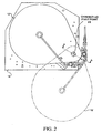
- Figure 2 is a cross-sectional view of the Figure 1 process module.
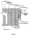
- Figure 3 is a top perspective view of the Figure 1 process module with the lid rotated about a chamber lid pivot point to allow for cleaning of an interior of the lid.
- Figure 4 is an exploded view of the Figure 1 process module including a hot plate assembly according to an embodiment of the present invention.
- Figure 5 is a cross-sectional view of a portion of the Figure 4 process module.
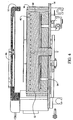
- Figure 6 is a full cross-sectional view of the Figure 4 process module.
- The present invention may be used in semiconductor manufacturing equipment. As illustrated in Figure 1,
assembly 10 includes alid 12, abase plate 14 and ahousing 16.Lid 12,base plate 14 andhousing 16 define a process chamber. - Referring now to Figures 2 and 3,
lid 12 is supported in a horizontal plane by ahorizontal guide 18 and avertical shaft 20 at alid pivot point 22. Shaft 20 is supported in abearing block 22 with two bushings 24. Togetherguide 18 and bushings 24 provide support forlid 12.Guide 18 is rigidly attached to a mountedblock 26 located onbase plate 14. - Lid's 12 open and close motion can be accomplished with a
pneumatic cylinder 28, or other suitable mechanical structure, attached betweenbearing block 22 andbase plate 14. Innormal operation lid 12 is constrained from rotating with a suitable device including but not limited to aretractable spring plunger 30 located onbearing block 22. In the up position,cylinder 28 is in its fully extended position.Lid 12 is supported in the horizontal plane by the reaction forces ofhorizontal guide 18 and bushings 24.Lid 12 can be cleaned or serviced in the "up" or open position. To rotatelid 12spring plunger 30 is retracted. Whenspring plunger 30 is retractedlid 12 can be rotated to a position allowing access to clean aninternal lid surfaces 32 which can include a shower head or other assembly that delivers a fluidic medium to the chamber.. - Bushings 24 allow
lid 12 to be rotated about a vertical pivot axis. Substantially constant contact withhorizontal guide 18 maintainslid 12 in a horizontal plane. Retractingspring plunger 30 and rotation oflid 12 is accomplished without removing or disassemblingassembly 12. A flexibleprocess gas tube 34 allows movement withlid 12 while remaining fixed (connected) at the opposite end. In the "down" or closed position, a chamber vacuum seal, such as O-ring 36, provides a vacuum tight boundary and sealing surface of the process chamber. A controlled clearance between the lid support shaft and the bushings allows the sealing surface of the lid to lie parallel a top ofhousing 16. Additionally, the design allows for a small amount of vertical axis relative motion between the lid support shaft and bearing block due to variations in pneumatic cylinder stroke length and compression of the vacuum seal. - Referring now to Figures 4 and 5,
process module assembly 10 is a bake module that includes aninsulator 38, one or morereflective members 40, ahot plate 42 andhousing 16.Reflective members 40 can have plate-type geometric configurations.Housing 16 has a diameter larger than the diameters ofhot plate 42 andinsulator 38, and a height that is approximately equal to the height ofinsulator 38 andhot plate 42.Lid 12 can include ashower head 44.Base plate 14 can include an exhaust port and an assembly to movelid 12, as described in Figures 2 and 3.Insulator 38 is positioned onbase plate 14 in a manner to create afirst air gap 46.First air gap 46 creates a conductive resistance layer betweenbase plate 14 and the remaining elements ofassembly 10. The diameter offirst air gap 46 can be smaller than the diameter ofinsulator 38. -
Insulator 38 has a top surface with arecess 48.Recess 48 is dimensioned to receive one or morereflective members 40. As illustrated in Figure 4, threereflective members 40 are included. It will be appreciated that the present invention can include onereflective member 40, or any number ofreflective members 40. Anair gap 50 is formed between a top surface ofinsulator 38 and the lower mostreflective member 40.Air gap 50 creates a conductive resistance layer. Air gaps are also formed between adjacentreflective members 40 to once again create conductive resistance layers. - The top surfaces of
reflective members 40 have high thermal reflectivity and low thermal absorptivity characteristics. The diameters ofreflective members 40 are slightly smaller than the diameter ofhot plate 42. - An
air gap 52 is formed betweenhousing 16 andinsulator 38 andhot plate 42. Hot gases surroundinghot plate 42 are removed by traveling fromgap 52 and then throughexhaust ports 54 that are formed ininsulator 38. -
Grooves housing 16. O-rings grooves ring 60 provides a seal betweenhousing 16 andbase plate 14, while O-ring 36 creates a seal betweenhousing 16 andlid 12. - Process gases can be introduced to
assembly 10 through agas conduit 66.Shower head 44 receives gases fromgas conduit 66 and injects the gases onto a top surface of a wafer positioned adjacent tohot plate 42. - It will be readily apparent to those skilled in the art that this invention is not limited to the embodiments described above. Different embodiments can be developed without departing from the scope of the invention as defined in the claims set forth below.
Claims (16)
- A hot plate assembly (10), comprising:a base plate (14);a lid (12);a housing (16) positioned between the base plate (14) and the lid (12), the housing (16), lid (12) and base plate (14) forming a process chamber;an insulator (38) positioned adjacent to the base plate (14) in the process chamber with a first air gap (46) formed at least partially between a bottom surface of the insulator (38) and a top surface of the base plate (14);a hot plate (42) positioned adjacent to the insulator in the process chamber; andat least a first reflective member (40) positioned between the hot plate (42) and the insulator (38); andan airgap (52) formed between the housing (16) and the insulator (38) and the hot plate (42);characterised in that said insulator (38) includes exhaust ports (54) whereby hot gases surrounding the hot plate (42) may be removed by travelling from the airgap (52) and then through said exhaust ports (54).
- The assembly (10) of claim 1, further comprising:a first fluid delivery member coupled to the lid (12), the first fluid delivery member being positioned in the process chamber when the lid (12) is sealed to the housing.
- The assembly (10) of claim 2, wherein the first fluid delivery member is a shower head.
- The assembly (10) of claim 2 or 3, further comprising:a flexible second fluid delivery member (34) extending from an exterior of the lid (12) and coupled to the first fluid delivery member.
- The assembly (10) of claim 4, wherein the flexible second fluid delivery member (34) is made of pliable material.
- The assembly (10) of any preceding claim, wherein the diameter of the first air gap (46) is less than the diameter of the insulator (38).
- The assembly (10) of any preceding claim, wherein the insulator (38) has a top surface that includes a recess (48).
- The assembly (10) of claim 7, wherein the first reflective member (40) is at least partially positioned in the recess (48).
- The assembly (10) of any one of claims 1 to 8, wherein at least a portion of the first reflective member (40) is sufficiently distanced from the insulator (38) to create an air gap between the insulator and the first reflective member.
- The assembly (10) of any preceding claim, further comprising:a second reflective member (40) positioned adjacent to the first reflective member (40).
- The assembly (10) of claim 10, wherein at least portions of the first and second reflective members (40) are sufficiently distanced to create an air gap between the first and second reflective members.
- The assembly (10) of claim 10 or 11, wherein each of the first and second reflective members (40) has a top surface facing the lid (12) and a bottom surface facing the base plate (14).
- The assembly (10) of claim 12, wherein each top surface of the first and second reflective members (40) has a high thermal reflectivity.
- The assembly (10) of claim 13, wherein each top surface of the first and second reflective members (40) has a low thermal absorptivity characteristic.
- The assembly (10) of any one of claims 10 to 14, wherein each of the first and second reflective members (40) has a diameter that is smaller than a diameter of the hot plate (42).
- The assembly (10) of any preceding claim, further comprising:an O-ring (36) that creates a seal between the housing (16) and the lid (12).
Priority Applications (1)
| Application Number | Priority Date | Filing Date | Title |
|---|---|---|---|
| EP05003989A EP1536457A2 (en) | 1999-06-16 | 2000-06-16 | Process chamber assembly with reflective hot plate |
Applications Claiming Priority (7)
| Application Number | Priority Date | Filing Date | Title |
|---|---|---|---|
| US13956099P | 1999-06-16 | 1999-06-16 | |
| US139560P | 1999-06-16 | ||
| US20361200P | 2000-05-10 | 2000-05-10 | |
| US203612P | 2000-05-10 | ||
| US593270 | 2000-06-13 | ||
| US09/593,270 US6416318B1 (en) | 1999-06-16 | 2000-06-13 | Process chamber assembly with reflective hot plate and pivoting lid |
| PCT/US2000/016635 WO2000077833A2 (en) | 1999-06-16 | 2000-06-16 | Process chamber assembly with reflective hot plate |
Related Child Applications (1)
| Application Number | Title | Priority Date | Filing Date |
|---|---|---|---|
| EP05003989A Division EP1536457A2 (en) | 1999-06-16 | 2000-06-16 | Process chamber assembly with reflective hot plate |
Publications (2)
| Publication Number | Publication Date |
|---|---|
| EP1186007A2 EP1186007A2 (en) | 2002-03-13 |
| EP1186007B1 true EP1186007B1 (en) | 2008-01-16 |
Family
ID=27385360
Family Applications (1)
| Application Number | Title | Priority Date | Filing Date |
|---|---|---|---|
| EP00941486A Expired - Lifetime EP1186007B1 (en) | 1999-06-16 | 2000-06-16 | Process chamber assembly with reflective hot plate |
Country Status (8)
| Country | Link |
|---|---|
| US (1) | US6416318B1 (en) |
| EP (1) | EP1186007B1 (en) |
| JP (1) | JP4045098B2 (en) |
| KR (2) | KR100537230B1 (en) |
| AT (1) | ATE384333T1 (en) |
| AU (1) | AU5619000A (en) |
| DE (1) | DE60037806T2 (en) |
| WO (1) | WO2000077833A2 (en) |
Families Citing this family (8)
| Publication number | Priority date | Publication date | Assignee | Title |
|---|---|---|---|---|
| US6838115B2 (en) * | 2000-07-12 | 2005-01-04 | Fsi International, Inc. | Thermal processing system and methods for forming low-k dielectric films suitable for incorporation into microelectronic devices |
| US20030173346A1 (en) * | 2002-03-18 | 2003-09-18 | Renken Wayne Glenn | System and method for heating and cooling wafer at accelerated rates |
| CN1682084A (en) * | 2002-09-10 | 2005-10-12 | Fsi国际公司 | Thermal process station with heated lid |
| US6891134B2 (en) * | 2003-02-10 | 2005-05-10 | Asml Netherlands B.V. | Integrally formed bake plate unit for use in wafer fabrication system |
| US6994544B2 (en) * | 2004-01-30 | 2006-02-07 | Texas Instruments Incorporated | Wafer scale thermal stress fixture and method |
| KR100601979B1 (en) * | 2004-12-30 | 2006-07-18 | 삼성전자주식회사 | Semiconductor Wafer Baking Apparatus |
| JP4827569B2 (en) * | 2006-03-23 | 2011-11-30 | 大日本スクリーン製造株式会社 | SUBSTRATE SUPPORT STRUCTURE, HEAT TREATMENT DEVICE USING THE SAME, SHEET PRODUCT USED FOR SUBSTRATE SUPPORT STRUCTURE, AND METHOD FOR PRODUCING SUBSTRATE SUPPORT STRUCTURE |
| US9581255B2 (en) | 2012-07-23 | 2017-02-28 | Henning, Inc. | Multiple proportion delivery systems and methods |
Family Cites Families (14)
| Publication number | Priority date | Publication date | Assignee | Title |
|---|---|---|---|---|
| JPS60119711A (en) | 1983-12-02 | 1985-06-27 | Hitachi Ltd | Vapor phase reaction unit |
| JPH07114185B2 (en) | 1986-11-05 | 1995-12-06 | 日本電気株式会社 | Substrate heating device |
| JPS63260146A (en) | 1987-04-17 | 1988-10-27 | Nippon Maikuronikusu:Kk | Measuring device for semiconductor wafer |
| JPH01310555A (en) * | 1988-06-08 | 1989-12-14 | Mitsubishi Electric Corp | Wafer housing case |
| US5011794A (en) * | 1989-05-01 | 1991-04-30 | At&T Bell Laboratories | Procedure for rapid thermal annealing of implanted semiconductors |
| JP3044735B2 (en) | 1990-03-30 | 2000-05-22 | ソニー株式会社 | Sputtering equipment |
| US5223113A (en) | 1990-07-20 | 1993-06-29 | Tokyo Electron Limited | Apparatus for forming reduced pressure and for processing object |
| JP2890087B2 (en) * | 1993-06-10 | 1999-05-10 | 東京エレクトロン株式会社 | Processing equipment |
| TW444922U (en) | 1994-09-29 | 2001-07-01 | Tokyo Electron Ltd | Heating device and the processing device using the same |
| DE19622322C2 (en) | 1995-06-15 | 1999-02-25 | Toshiba Ceramics Co | Vapor phase growing apparatus |
| US5885353A (en) * | 1996-06-21 | 1999-03-23 | Micron Technology, Inc. | Thermal conditioning apparatus |
| US5756157A (en) * | 1996-10-02 | 1998-05-26 | Silicon Valley Group | Method for processing flat panel displays and large wafers |
| US6050446A (en) | 1997-07-11 | 2000-04-18 | Applied Materials, Inc. | Pivoting lid assembly for a chamber |
| US6086362A (en) * | 1998-05-20 | 2000-07-11 | Applied Komatsu Technology, Inc. | Multi-function chamber for a substrate processing system |
-
2000
- 2000-06-13 US US09/593,270 patent/US6416318B1/en not_active Expired - Lifetime
- 2000-06-16 EP EP00941486A patent/EP1186007B1/en not_active Expired - Lifetime
- 2000-06-16 JP JP2001503215A patent/JP4045098B2/en not_active Expired - Fee Related
- 2000-06-16 DE DE60037806T patent/DE60037806T2/en not_active Expired - Lifetime
- 2000-06-16 KR KR10-2001-7016169A patent/KR100537230B1/en not_active Expired - Lifetime
- 2000-06-16 KR KR1020057005866A patent/KR100564889B1/en not_active Expired - Lifetime
- 2000-06-16 AT AT00941486T patent/ATE384333T1/en not_active IP Right Cessation
- 2000-06-16 AU AU56190/00A patent/AU5619000A/en not_active Abandoned
- 2000-06-16 WO PCT/US2000/016635 patent/WO2000077833A2/en not_active Ceased
Also Published As
| Publication number | Publication date |
|---|---|
| AU5619000A (en) | 2001-01-02 |
| US6416318B1 (en) | 2002-07-09 |
| KR100537230B1 (en) | 2005-12-16 |
| KR100564889B1 (en) | 2006-03-30 |
| DE60037806T2 (en) | 2009-01-15 |
| KR20050053735A (en) | 2005-06-08 |
| KR20020019088A (en) | 2002-03-09 |
| EP1186007A2 (en) | 2002-03-13 |
| JP2003502838A (en) | 2003-01-21 |
| WO2000077833A2 (en) | 2000-12-21 |
| ATE384333T1 (en) | 2008-02-15 |
| DE60037806D1 (en) | 2008-03-06 |
| JP4045098B2 (en) | 2008-02-13 |
| WO2000077833A3 (en) | 2001-07-12 |
Similar Documents
| Publication | Publication Date | Title |
|---|---|---|
| JP4473144B2 (en) | Bushing for substrate support | |
| US7722925B2 (en) | Showerhead mounting to accommodate thermal expansion | |
| US20230420279A1 (en) | Substrate transfer mechanism to reduce back-side substrate contact | |
| KR100940958B1 (en) | Wafer Transport Unit | |
| US6368450B2 (en) | Processing apparatus | |
| US5753133A (en) | Method and apparatus for etching film layers on large substrates | |
| US6303906B1 (en) | Resistively heated single wafer furnace | |
| JP2024539714A (en) | Chemical vapor deposition apparatus and method | |
| KR100399167B1 (en) | Vacuum Heat Transfer Station without Clamp | |
| US6416318B1 (en) | Process chamber assembly with reflective hot plate and pivoting lid | |
| US20010040230A1 (en) | Compact gate valve | |
| KR20020010681A (en) | Vacuum processing apparatus | |
| US20040045813A1 (en) | Wafer processing apparatus, wafer stage, and wafer processing method | |
| US6091056A (en) | Hot plate oven for processing flat panel displays and large wafers | |
| JP3908678B2 (en) | Wafer processing method | |
| US6698718B2 (en) | Rotary valve | |
| EP1536457A2 (en) | Process chamber assembly with reflective hot plate | |
| JP3617860B2 (en) | Substrate processing method and substrate processing apparatus | |
| JP2004087869A (en) | Wafer processing apparatus, wafer stage and wafer processing method | |
| CN112542410B (en) | Reactor | |
| JPH04330722A (en) | wafer processing equipment | |
| US20250372408A1 (en) | Valve apparatuses and related methods for reactive process gas isolation and facilitating purge during isolation | |
| US20260126118A1 (en) | Valve apparatuses and related methods for wafer transfer in a semiconductor processing system | |
| WO2008096981A1 (en) | Apparatus for forming a layer |
Legal Events
| Date | Code | Title | Description |
|---|---|---|---|
| PUAI | Public reference made under article 153(3) epc to a published international application that has entered the european phase |
Free format text: ORIGINAL CODE: 0009012 |
|
| 17P | Request for examination filed |
Effective date: 20011128 |
|
| AK | Designated contracting states |
Kind code of ref document: A2 Designated state(s): AT BE CH CY DE DK ES FI FR GB GR IE IT LI LU MC NL PT SE |
|
| AX | Request for extension of the european patent |
Free format text: AL;LT;LV;MK;RO;SI |
|
| 17Q | First examination report despatched |
Effective date: 20040827 |
|
| RAP1 | Party data changed (applicant data changed or rights of an application transferred) |
Owner name: ASML US, INC. |
|
| RAP1 | Party data changed (applicant data changed or rights of an application transferred) |
Owner name: ASML HOLDING N.V. |
|
| GRAP | Despatch of communication of intention to grant a patent |
Free format text: ORIGINAL CODE: EPIDOSNIGR1 |
|
| GRAS | Grant fee paid |
Free format text: ORIGINAL CODE: EPIDOSNIGR3 |
|
| GRAA | (expected) grant |
Free format text: ORIGINAL CODE: 0009210 |
|
| AK | Designated contracting states |
Kind code of ref document: B1 Designated state(s): AT BE CH CY DE DK ES FI FR GB GR IE IT LI LU MC NL PT SE |
|
| REG | Reference to a national code |
Ref country code: GB Ref legal event code: FG4D |
|
| REG | Reference to a national code |
Ref country code: CH Ref legal event code: EP |
|
| REG | Reference to a national code |
Ref country code: IE Ref legal event code: FG4D |
|
| REF | Corresponds to: |
Ref document number: 60037806 Country of ref document: DE Date of ref document: 20080306 Kind code of ref document: P |
|
| PG25 | Lapsed in a contracting state [announced via postgrant information from national office to epo] |
Ref country code: FI Free format text: LAPSE BECAUSE OF FAILURE TO SUBMIT A TRANSLATION OF THE DESCRIPTION OR TO PAY THE FEE WITHIN THE PRESCRIBED TIME-LIMIT Effective date: 20080116 Ref country code: CH Free format text: LAPSE BECAUSE OF FAILURE TO SUBMIT A TRANSLATION OF THE DESCRIPTION OR TO PAY THE FEE WITHIN THE PRESCRIBED TIME-LIMIT Effective date: 20080116 Ref country code: ES Free format text: LAPSE BECAUSE OF FAILURE TO SUBMIT A TRANSLATION OF THE DESCRIPTION OR TO PAY THE FEE WITHIN THE PRESCRIBED TIME-LIMIT Effective date: 20080427 Ref country code: LI Free format text: LAPSE BECAUSE OF FAILURE TO SUBMIT A TRANSLATION OF THE DESCRIPTION OR TO PAY THE FEE WITHIN THE PRESCRIBED TIME-LIMIT Effective date: 20080116 |
|
| REG | Reference to a national code |
Ref country code: CH Ref legal event code: PL |
|
| PG25 | Lapsed in a contracting state [announced via postgrant information from national office to epo] |
Ref country code: AT Free format text: LAPSE BECAUSE OF FAILURE TO SUBMIT A TRANSLATION OF THE DESCRIPTION OR TO PAY THE FEE WITHIN THE PRESCRIBED TIME-LIMIT Effective date: 20080116 |
|
| ET | Fr: translation filed | ||
| PG25 | Lapsed in a contracting state [announced via postgrant information from national office to epo] |
Ref country code: PT Free format text: LAPSE BECAUSE OF FAILURE TO SUBMIT A TRANSLATION OF THE DESCRIPTION OR TO PAY THE FEE WITHIN THE PRESCRIBED TIME-LIMIT Effective date: 20080616 Ref country code: BE Free format text: LAPSE BECAUSE OF FAILURE TO SUBMIT A TRANSLATION OF THE DESCRIPTION OR TO PAY THE FEE WITHIN THE PRESCRIBED TIME-LIMIT Effective date: 20080116 |
|
| PGFP | Annual fee paid to national office [announced via postgrant information from national office to epo] |
Ref country code: IT Payment date: 20080623 Year of fee payment: 9 |
|
| PG25 | Lapsed in a contracting state [announced via postgrant information from national office to epo] |
Ref country code: SE Free format text: LAPSE BECAUSE OF FAILURE TO SUBMIT A TRANSLATION OF THE DESCRIPTION OR TO PAY THE FEE WITHIN THE PRESCRIBED TIME-LIMIT Effective date: 20080416 Ref country code: DK Free format text: LAPSE BECAUSE OF FAILURE TO SUBMIT A TRANSLATION OF THE DESCRIPTION OR TO PAY THE FEE WITHIN THE PRESCRIBED TIME-LIMIT Effective date: 20080116 |
|
| PGFP | Annual fee paid to national office [announced via postgrant information from national office to epo] |
Ref country code: NL Payment date: 20080618 Year of fee payment: 9 |
|
| PLBE | No opposition filed within time limit |
Free format text: ORIGINAL CODE: 0009261 |
|
| STAA | Information on the status of an ep patent application or granted ep patent |
Free format text: STATUS: NO OPPOSITION FILED WITHIN TIME LIMIT |
|
| 26N | No opposition filed |
Effective date: 20081017 |
|
| PGFP | Annual fee paid to national office [announced via postgrant information from national office to epo] |
Ref country code: GB Payment date: 20080620 Year of fee payment: 9 |
|
| PG25 | Lapsed in a contracting state [announced via postgrant information from national office to epo] |
Ref country code: MC Free format text: LAPSE BECAUSE OF NON-PAYMENT OF DUE FEES Effective date: 20080630 |
|
| PG25 | Lapsed in a contracting state [announced via postgrant information from national office to epo] |
Ref country code: IE Free format text: LAPSE BECAUSE OF NON-PAYMENT OF DUE FEES Effective date: 20080616 |
|
| PG25 | Lapsed in a contracting state [announced via postgrant information from national office to epo] |
Ref country code: CY Free format text: LAPSE BECAUSE OF FAILURE TO SUBMIT A TRANSLATION OF THE DESCRIPTION OR TO PAY THE FEE WITHIN THE PRESCRIBED TIME-LIMIT Effective date: 20080116 |
|
| GBPC | Gb: european patent ceased through non-payment of renewal fee |
Effective date: 20090616 |
|
| NLV4 | Nl: lapsed or anulled due to non-payment of the annual fee |
Effective date: 20100101 |
|
| PG25 | Lapsed in a contracting state [announced via postgrant information from national office to epo] |
Ref country code: GB Free format text: LAPSE BECAUSE OF NON-PAYMENT OF DUE FEES Effective date: 20090616 |
|
| PG25 | Lapsed in a contracting state [announced via postgrant information from national office to epo] |
Ref country code: NL Free format text: LAPSE BECAUSE OF NON-PAYMENT OF DUE FEES Effective date: 20100101 Ref country code: LU Free format text: LAPSE BECAUSE OF NON-PAYMENT OF DUE FEES Effective date: 20080616 |
|
| PG25 | Lapsed in a contracting state [announced via postgrant information from national office to epo] |
Ref country code: GR Free format text: LAPSE BECAUSE OF FAILURE TO SUBMIT A TRANSLATION OF THE DESCRIPTION OR TO PAY THE FEE WITHIN THE PRESCRIBED TIME-LIMIT Effective date: 20080417 |
|
| PG25 | Lapsed in a contracting state [announced via postgrant information from national office to epo] |
Ref country code: IT Free format text: LAPSE BECAUSE OF NON-PAYMENT OF DUE FEES Effective date: 20090616 |
|
| REG | Reference to a national code |
Ref country code: FR Ref legal event code: PLFP Year of fee payment: 17 |
|
| REG | Reference to a national code |
Ref country code: FR Ref legal event code: PLFP Year of fee payment: 18 |
|
| REG | Reference to a national code |
Ref country code: FR Ref legal event code: PLFP Year of fee payment: 19 |
|
| PGFP | Annual fee paid to national office [announced via postgrant information from national office to epo] |
Ref country code: DE Payment date: 20190619 Year of fee payment: 20 |
|
| PGFP | Annual fee paid to national office [announced via postgrant information from national office to epo] |
Ref country code: FR Payment date: 20190619 Year of fee payment: 20 |
|
| REG | Reference to a national code |
Ref country code: DE Ref legal event code: R071 Ref document number: 60037806 Country of ref document: DE |