EP1185086A1 - A deflection circuit with a retrace capacitive transformation - Google Patents
A deflection circuit with a retrace capacitive transformation Download PDFInfo
- Publication number
- EP1185086A1 EP1185086A1 EP01402193A EP01402193A EP1185086A1 EP 1185086 A1 EP1185086 A1 EP 1185086A1 EP 01402193 A EP01402193 A EP 01402193A EP 01402193 A EP01402193 A EP 01402193A EP 1185086 A1 EP1185086 A1 EP 1185086A1
- Authority
- EP
- European Patent Office
- Prior art keywords
- retrace
- deflection
- coupled
- capacitance
- pulse voltage
- Prior art date
- Legal status (The legal status is an assumption and is not a legal conclusion. Google has not performed a legal analysis and makes no representation as to the accuracy of the status listed.)
- Withdrawn
Links
- 230000009466 transformation Effects 0.000 title claims abstract description 13
- 238000004804 winding Methods 0.000 claims abstract description 34
- 230000000737 periodic effect Effects 0.000 claims 2
- 239000003990 capacitor Substances 0.000 description 48
- 230000015556 catabolic process Effects 0.000 description 3
- 238000007493 shaping process Methods 0.000 description 2
- 241000226585 Antennaria plantaginifolia Species 0.000 description 1
- CLSVJBIHYWPGQY-UHFFFAOYSA-N [3-(2,5-dimethylphenyl)-8-methoxy-2-oxo-1-azaspiro[4.5]dec-3-en-4-yl] ethyl carbonate Chemical compound CCOC(=O)OC1=C(C=2C(=CC=C(C)C=2)C)C(=O)NC11CCC(OC)CC1 CLSVJBIHYWPGQY-UHFFFAOYSA-N 0.000 description 1
- 239000004020 conductor Substances 0.000 description 1
- 230000007423 decrease Effects 0.000 description 1
- 238000007599 discharging Methods 0.000 description 1
- 238000002955 isolation Methods 0.000 description 1
- 238000011084 recovery Methods 0.000 description 1
Images


Classifications
-
- H—ELECTRICITY
- H04—ELECTRIC COMMUNICATION TECHNIQUE
- H04N—PICTORIAL COMMUNICATION, e.g. TELEVISION
- H04N3/00—Scanning details of television systems; Combination thereof with generation of supply voltages
- H04N3/10—Scanning details of television systems; Combination thereof with generation of supply voltages by means not exclusively optical-mechanical
- H04N3/16—Scanning details of television systems; Combination thereof with generation of supply voltages by means not exclusively optical-mechanical by deflecting electron beam in cathode-ray tube, e.g. scanning corrections
- H04N3/22—Circuits for controlling dimensions, shape or centering of picture on screen
- H04N3/23—Distortion correction, e.g. for pincushion distortion correction, S-correction
- H04N3/233—Distortion correction, e.g. for pincushion distortion correction, S-correction using active elements
-
- H—ELECTRICITY
- H04—ELECTRIC COMMUNICATION TECHNIQUE
- H04N—PICTORIAL COMMUNICATION, e.g. TELEVISION
- H04N3/00—Scanning details of television systems; Combination thereof with generation of supply voltages
- H04N3/10—Scanning details of television systems; Combination thereof with generation of supply voltages by means not exclusively optical-mechanical
- H04N3/16—Scanning details of television systems; Combination thereof with generation of supply voltages by means not exclusively optical-mechanical by deflecting electron beam in cathode-ray tube, e.g. scanning corrections
-
- H—ELECTRICITY
- H04—ELECTRIC COMMUNICATION TECHNIQUE
- H04N—PICTORIAL COMMUNICATION, e.g. TELEVISION
- H04N3/00—Scanning details of television systems; Combination thereof with generation of supply voltages
- H04N3/10—Scanning details of television systems; Combination thereof with generation of supply voltages by means not exclusively optical-mechanical
- H04N3/16—Scanning details of television systems; Combination thereof with generation of supply voltages by means not exclusively optical-mechanical by deflecting electron beam in cathode-ray tube, e.g. scanning corrections
- H04N3/18—Generation of supply voltages, in combination with electron beam deflecting
Definitions
- the invention relates to a deflection circuit of a cathode ray tube (CRT).
- CRT cathode ray tube
- a typical horizontal deflection circuit for a CRT includes a horizontal deflection winding of a deflection yoke coupled in parallel with a retrace capacitance provided by, for example, a retrace capacitor.
- a horizontal output or switching transistor operating at a horizontal deflection frequency is coupled across the retrace capacitor.
- a supply voltage is coupled to the switching transistor and to the retrace capacitor via a supply inductance.
- the effective retrace capacitance required to produce the same deflection current amplitude would have to be smaller when a higher deflection frequency is utilized than when a lower deflection frequency is utilized. Therefore, the flyback pulse voltage developed across a horizontal output transistor would have to be higher at the higher deflection frequency.
- the maximum flyback pulse voltage that is permitted to develop across a horizontal output transistor limits the allowable, maximum horizontal frequency that can be utilized. Therefore, it may be desirable to reduce the effective retrace capacitance without substantially increasing the flyback pulse voltage developed across the horizontal output transistor.
- a horizontal deflection circuit embodying an inventive feature, includes switched, first and second retrace capacitors coupled in series with a deflection winding.
- First and second switching transistors are coupled across the first and second retrace capacitors, respectively.
- a supply voltage is coupled via a supply inductance to a junction terminal between the retrace capacitors.
- the switching transistors are switched off, during retrace, to produce a first retrace pulse voltage across the first retrace capacitance and a second retrace pulse voltage across the second retrace capacitance.
- the retrace pulse voltage across the deflection winding is equal to the sum of a first retrace pulse voltage and the second retrace pulse voltage and is larger than each.
- the retrace pulse voltage across the deflection winding is proportional to a ratio of the capacitances of the first and second capacitances. Thereby, capacitive transformation is obtained.
- a voltage across an S-shaping capacitor that is coupled in series with the deflection winding is also proportional to a ratio of the capacitances of the first and second capacitances.
- the peak voltage developed across each of the switching transistors is substantially smaller than the sum retrace pulse voltage developed across the deflection winding.
- the maximum scan frequency that can be employed is, advantageously, higher than in a deflection circuit in which the entire retrace pulse voltage across the deflection winding is developed across a single switching transistor.
- a horizontal deflection circuit includes an East-West raster distortion correction circuit for correcting pincushion raster distortion.
- Switched, first and second retrace capacitors are provided for providing the aforementioned capacitive transformation.
- the retrace switching timing of each one of the switching transistors remains the same relative to that of the other one of the switching transistors.
- a video display deflection apparatus includes a first retrace capacitance and a second retrace capacitance.
- a deflection winding is coupled to the first and second retrace capacitances to form a resonant circuit with the first and second retrace capacitances, during retrace.
- a first switching transistor is coupled to the first retrace capacitance for generating a first retrace pulse voltage in the resonant circuit.
- a second switching transistor is coupled to the second retrace capacitance for generating a second retrace pulse voltage in the second retrace capacitance.
- the first and second retrace pulse voltage are applied to the deflection winding in a manner to provide for retrace capacitance transformation.
- the second switching transistor is responsive to the first retrace pulse voltage for controlling, in accordance with the first retrace pulse voltage, when a switching operation occurs in the second switching transistor.
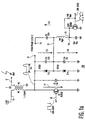
- a deflection circuit 100 of FIGURE 1a when combined with an arrangement 100b of FIGURE 1b, operates at a horizontal frequency of 3 times fH and a period one third of H.
- fH denotes the horizontal frequency in a television standard such as 15,525 KHz.
- H denotes the horizontal period in the television standard.
- Deflection circuit 100 of FIGURE 1a includes a primary winding W1 coupled to a source of a constant value supply voltage B+. Winding W1 of a conventional flyback transformer T is also coupled to a horizontal output or switching transistor Q1 controlled by a horizontal drive signal 50 having approximately 50% duty cycle. An emitter voltage of transistor Q1 is at a common conductor potential, or ground. A junction terminal 51 of winding W1 and a collector of transistor Q1 is coupled to a retrace capacitor C1a. A retrace capacitor Cb is coupled to terminal 51 and in parallel with transistor Q1. A terminal 52 of capacitor C1a is coupled to a retrace capacitor C1b. A conventional damper diode D1a is coupled in parallel with capacitor C1a.
- a conventional damper diode D1b is coupled in parallel with capacitor C1b.
- Junction terminal 52 is coupled to a conventional East-West modulation inductor Lew.
- Inductor Lew has a terminal 53 that is coupled to a collector of a conventional East-West modulation and to a conventional filter capacitor Cew to form a diode modulator.
- Transistor QEW is controlled in a conventional manner by a vertical rate East-West modulation signal E/W-DRIVE having a period V. Period V denotes the vertical period in the television standard such as 16.6 milisecond.
- a feedback resistor transistor Rew is coupled between the collector and base of transistor QEW to provide operation in class A mode of operation.
- a vertical rate modulation voltage Vm is developed at terminal 53, in a conventional manner.
- a conventional S-shaping capacitor Cs is coupled between terminal 52 and a terminal 54.
- a deflection winding Ly of FIGURE 1b is coupled to a switched, retrace capacitor C2 to form a series arrangement between terminals 51 and 54.
- a switching transistor Q2 is coupled in parallel with capacitor C2 for switching capacitor C2.
- a return recovery current in transistor Q2 is performed by the operation of an integrally formed damper diode, not shown, formed with transistor Q2 in the same integrated circuit.
- FIGURES 2a-2d illustrate waveforms useful for explaining the operation of the circuit of FIGURES 1a and 1b. Each waveform is applicable to a corresponding horizontal period H/3. Similar symbols and numerals in FIGURES 1a, 1b and 2a-2d indicate similar items or functions.
- Transistor Q1 of FIGURE 1a is turned off to form a retrace resonant circuit that includes deflection winding Ly of FIGURE 1b and capacitor C1a of FIGURE 1a, during retrace.
- a resonant retrace pulse voltage V1 having a period H/3 is developed at terminal 51 of winding Ly.
- Voltage V1 is generated when a collector current iQ1 of FIGURE 2a of transistor Q1 of FIGURE 1a abruptly drops to zero.
- Pulse voltage V1 of FIGURE 2c is coupled to transformer T of FIGURE 1a for producing an ultor voltage U.
- pulse voltage V1 developed at terminal 51 is applied to a current path formed by a power supply filter capacitor C101, a capacitor C3, a resistor R2, a resistor R1 and an internal gate-source capacitance, not shown, of transistor Q2.
- a supply voltage V+12 of 12V is developed in capacitor C101.
- Resistor R2 is coupled between an emitter of transistor Q3 and terminal 61.
- Terminal 62 forms a junction terminal for the emitter of a transistor Q3, resistor R1 and resistor R2.
- the voltage produced at terminal 61 of resistor R2 is coupled to the base of transistor Q3 via a diode D4 when diode D4 is forward biased to turn on transistor Q3.
- transistor Q3 When transistor Q3 is turned on, a positive charged, gate-source capacitance, not shown, of transistor Q2 that maintains transistor Q2 conductive is quickly discharged via a current path formed by transistor Q3 and resistor R1. Then, transistor Q2 turns off and remains in the turned-off state for the entire remainder of a retrace interval TRET of FIGURES 2a-2d. Thereby, a retrace pulse voltage V2 of FIGURE 1b is generated in capacitor C2. Voltage V2 of FIGURE 2c is generated when a collector current iQ2 of FIGURE 2b of transistor Q2 of FIGURE 1b abruptly drops to zero.
- a combined retrace pulse voltage VLy, developed across deflection winding Ly of FIGURE1a, is equal to the sum of retrace pulse voltage Via of FIGURE 1a, developed in retrace capacitor C1a, and retrace pulse voltage V2 of FIGURE 1b, developed in retrace capacitor C2.
- Pulse voltage VLy is larger than each of pulse voltage V2 and pulse voltage Via of FIGURE 1a.
- the peak of pulse voltages V1, developed across switching transistor Q1 is substantially smaller than voltage VLy. Therefore, for a given inductance of winding Ly of FIGURE 1b and a breakdown voltage of switching transistor Q1 of FIGURE1a, the scan frequency that can be employed is advantageously higher.
- the scan frequency that can be employed is higher than if retrace pulse voltage VLy of FIGURE 1b were developed entirely across switching transistor Q1 of FIGURE 1a. The result is that retrace capacitor transformation is obtained.
- Circuit 100 of FIGURE 1a that is coupled to circuit 100b of FIGURE 1b provides capacitive transformation that is, advantageously, constant throughout vertical trace.
- the inductance of winding W1 is large or infinite.
- VmAv represents the average value of voltage Vm.
- (1 + the value of capacitor C1a / the value of capacitor C2 ) represents the capacitive transformation factor.
- voltage VCs is larger for a given difference between voltage B+ and the average value of voltage Vm.
- the increased average value of voltage VCs enables the generation of a given amplitude of deflection current iy at a higher deflection frequency.
- the effective retrace capacitance is smaller. Smaller retrace capacitance results in a shorter retrace interval TRET of FIGURES 2a-2d.
- diodes D1a and D1b are conductive in a conventional manner. Additionally, the integrally formed damper diode, not shown, of transistor Q2 of FIGURE 1b is also conductive. During the second half of trace, transistor Q1 of FIGURE 1a is turned on, in a conventional manner.
- transistor Q2 After a short delay time determined by the gate-source capacitance, not shown, of transistor Q2, transistor Q2 is turned on to form a low drain-source resistance. This low resistance is placed in parallel with the integrally formed, forward biased damper diode, not shown, of transistor Q2 for a portion of the trace interval similar to the turn on interval in transistor Q1 of FIGURE 1a. Diode D5 of FIGURE 1b protects transistor Q2 from excessive gate voltage.
- a phase between retrace voltage V1 of FIGURE 2c and retrace voltage V2 remains the same in each horizontal deflection cycle, throughout vertical interval V.
- retrace interval TRET has the same width, throughout vertical interval V.
- deflection circuit 100 of FIGURE 1a is coupled to the arrangement of a booster circuit 100c of FIGURE 1c, instead of circuit 100b in FIGURE 1b.
- Similar symbols and numerals in FIGURE 1c, except for the prime symbol ('), and in FIGURES 1a, 1b and 2a-2d indicate similar items or functions.
- Deflection winding Ly' of FIGURE 1c is interposed between a capacitor C2' and capacitor C1a of FIGURE 1a.
- circuit 100c of FIGURE 1c divides a retrace pulse voltage VLy', across winding Ly', into a positive voltage with respect to ground, at terminal 51, and a symmetrical, negative voltage with respect to ground, at terminal 54.
- VLy' retrace pulse voltage
- VLy' retrace pulse voltage
- VLy' retrace pulse voltage across winding Ly'
- the peak of each retrace pulse voltage at terminals 51 and 54 with respect to ground is smaller than the peak of their sum. Therefore, advantageously, less demanding electrical isolation is required than in the combined arrangement of FIGURES 1a and 1b that provides a non-symmetrically driven arrangement.
- a capacitor C3' of FIGURE 1c is used for sensing an occurrence of retrace pulse voltage V1 at terminal 51, similarly to the way done in FIGURE 1b.
- a forward biased diode D4' of FIGURE 1c coupled in series with capacitor C3' and a capacitor C4' causes a transistor Q3' to conduct by charging capacitor C4'. Consequently, a positive charged gate-source capacitance, not shown, of a transistor Q2' is quickly discharged via a resistor R1' and transistor Q3'. Transistor Q2' turns off and remains turned off for the entire remainder of retrace.
- capacitor C3' FIGURE 1c discharges via a diode D3', resistor R1', a forward biased D5' and deflection winding Ly'.
- Diode D3 is coupled in an anti-parralel manner with respect to diode D4'. Because capacitor C4' is not included in the retrace discharge current path of capacitor C3', the energy in capacitor C4' is maintained stored, during retrace. Transistor Q3' remains non-conductive because no base current is produced, during the second half of retrace.
- capacitor C4' starts discharging.
- a diode D6' that is coupled between the base of transistor Q3' and winding Ly' is forward biased.
- Capacitor C4' now a voltage source, charges the gate-source capacitance, not shown, of transistor Q2' via a resistor R2'.
- Transistor Q2' turns on after a delay time similar to that in FIGURE 1b.
- a diode D5' also performs similar protection function to that described with respect to diode D5 in FIGURE 1b.
Landscapes
- Engineering & Computer Science (AREA)
- Multimedia (AREA)
- Signal Processing (AREA)
- Details Of Television Scanning (AREA)
Abstract
Description
- The invention relates to a deflection circuit of a cathode ray tube (CRT).
- A typical horizontal deflection circuit for a CRT includes a horizontal deflection winding of a deflection yoke coupled in parallel with a retrace capacitance provided by, for example, a retrace capacitor. A horizontal output or switching transistor operating at a horizontal deflection frequency is coupled across the retrace capacitor. A supply voltage is coupled to the switching transistor and to the retrace capacitor via a supply inductance.
- For a given deflection winding inductance and a supply voltage magnitude, the effective retrace capacitance required to produce the same deflection current amplitude would have to be smaller when a higher deflection frequency is utilized than when a lower deflection frequency is utilized. Therefore, the flyback pulse voltage developed across a horizontal output transistor would have to be higher at the higher deflection frequency. For a given switching transistor breakdown voltage characteristic, the maximum flyback pulse voltage that is permitted to develop across a horizontal output transistor limits the allowable, maximum horizontal frequency that can be utilized. Therefore, it may be desirable to reduce the effective retrace capacitance without substantially increasing the flyback pulse voltage developed across the horizontal output transistor.
- A horizontal deflection circuit, embodying an inventive feature, includes switched, first and second retrace capacitors coupled in series with a deflection winding. First and second switching transistors are coupled across the first and second retrace capacitors, respectively. A supply voltage is coupled via a supply inductance to a junction terminal between the retrace capacitors. The switching transistors are switched off, during retrace, to produce a first retrace pulse voltage across the first retrace capacitance and a second retrace pulse voltage across the second retrace capacitance. The retrace pulse voltage across the deflection winding is equal to the sum of a first retrace pulse voltage and the second retrace pulse voltage and is larger than each. The retrace pulse voltage across the deflection winding is proportional to a ratio of the capacitances of the first and second capacitances. Thereby, capacitive transformation is obtained. Similarly, a voltage across an S-shaping capacitor that is coupled in series with the deflection winding is also proportional to a ratio of the capacitances of the first and second capacitances.
- Advantageously, the peak voltage developed across each of the switching transistors is substantially smaller than the sum retrace pulse voltage developed across the deflection winding. The result is that, for a given switching transistor breakdown voltage characteristic, the maximum scan frequency that can be employed is, advantageously, higher than in a deflection circuit in which the entire retrace pulse voltage across the deflection winding is developed across a single switching transistor.
- A horizontal deflection circuit, embodying an inventive feature, includes an East-West raster distortion correction circuit for correcting pincushion raster distortion. Switched, first and second retrace capacitors are provided for providing the aforementioned capacitive transformation. Throughout a given vertical trace interval, the retrace switching timing of each one of the switching transistors remains the same relative to that of the other one of the switching transistors. Thereby, advantageously, East-West raster distortion correction is obtained in a manner that avoids producing retrace time modulation.
- A video display deflection apparatus, embodying an inventive feature, includes a first retrace capacitance and a second retrace capacitance. A deflection winding is coupled to the first and second retrace capacitances to form a resonant circuit with the first and second retrace capacitances, during retrace. A first switching transistor is coupled to the first retrace capacitance for generating a first retrace pulse voltage in the resonant circuit. A second switching transistor is coupled to the second retrace capacitance for generating a second retrace pulse voltage in the second retrace capacitance. The first and second retrace pulse voltage are applied to the deflection winding in a manner to provide for retrace capacitance transformation. The second switching transistor is responsive to the first retrace pulse voltage for controlling, in accordance with the first retrace pulse voltage, when a switching operation occurs in the second switching transistor.
-
- FIGURE 1a and 1b illustrate a combined deflection circuit, embodying a first inventive feature;
- FIGURE 1a and 1c illustrate a combined deflection circuit, embodying a second inventive feature; and
- FIGURES 2a, 2b, 2c and 2d illustrate waveforms useful for explaining the operation of the combined circuit of FIGURE 1a and 1b.
-
- A
deflection circuit 100 of FIGURE 1a, when combined with anarrangement 100b of FIGURE 1b, operates at a horizontal frequency of 3 times fH and a period one third of H. The term fH denotes the horizontal frequency in a television standard such as 15,525 KHz. Similarly, the term H denotes the horizontal period in the television standard.. -
Deflection circuit 100 of FIGURE 1a includes a primary winding W1 coupled to a source of a constant value supply voltage B+. Winding W1 of a conventional flyback transformer T is also coupled to a horizontal output or switching transistor Q1 controlled by ahorizontal drive signal 50 having approximately 50% duty cycle. An emitter voltage of transistor Q1 is at a common conductor potential, or ground. Ajunction terminal 51 of winding W1 and a collector of transistor Q1 is coupled to a retrace capacitor C1a. A retrace capacitor Cb is coupled toterminal 51 and in parallel with transistor Q1. Aterminal 52 of capacitor C1a is coupled to a retrace capacitor C1b. A conventional damper diode D1a is coupled in parallel with capacitor C1a. A conventional damper diode D1b is coupled in parallel with capacitor C1b.Junction terminal 52 is coupled to a conventional East-West modulation inductor Lew. Inductor Lew has aterminal 53 that is coupled to a collector of a conventional East-West modulation and to a conventional filter capacitor Cew to form a diode modulator. Transistor QEW is controlled in a conventional manner by a vertical rate East-West modulation signal E/W-DRIVE having a period V. Period V denotes the vertical period in the television standard such as 16.6 milisecond. A feedback resistor transistor Rew is coupled between the collector and base of transistor QEW to provide operation in class A mode of operation. A vertical rate modulation voltage Vm is developed atterminal 53, in a conventional manner. A conventional S-shaping capacitor Cs is coupled betweenterminal 52 and aterminal 54. - A deflection winding Ly of FIGURE 1b is coupled to a switched, retrace capacitor C2 to form a series arrangement between
terminals - FIGURES 2a-2d illustrate waveforms useful for explaining the operation of the circuit of FIGURES 1a and 1b. Each waveform is applicable to a corresponding horizontal period H/3. Similar symbols and numerals in FIGURES 1a, 1b and 2a-2d indicate similar items or functions.
- Transistor Q1 of FIGURE 1a is turned off to form a retrace resonant circuit that includes deflection winding Ly of FIGURE 1b and capacitor C1a of FIGURE 1a, during retrace. A resonant retrace pulse voltage V1 having a period H/3 is developed at
terminal 51 of winding Ly. As shown in FIGURE 2c, Voltage V1 is generated when a collector current iQ1 of FIGURE 2a of transistor Q1 of FIGURE 1a abruptly drops to zero. Pulse voltage V1 of FIGURE 2c is coupled to transformer T of FIGURE 1a for producing an ultor voltage U. - In carrying out an inventive feature, pulse voltage V1 developed at
terminal 51 is applied to a current path formed by a power supply filter capacitor C101, a capacitor C3, a resistor R2, a resistor R1 and an internal gate-source capacitance, not shown, of transistor Q2. A supply voltage V+12 of 12V is developed in capacitor C101. As a result of pulse voltage V1, a positive voltage is produced at aterminal 62 of resistor R2 relative to that at aterminal 61 of resistor R2. Resistor R2 is coupled between an emitter of transistor Q3 andterminal 61.Terminal 62 forms a junction terminal for the emitter of a transistor Q3, resistor R1 and resistor R2. The voltage produced atterminal 61 of resistor R2 is coupled to the base of transistor Q3 via a diode D4 when diode D4 is forward biased to turn on transistor Q3. - When transistor Q3 is turned on, a positive charged, gate-source capacitance, not shown, of transistor Q2 that maintains transistor Q2 conductive is quickly discharged via a current path formed by transistor Q3 and resistor R1. Then, transistor Q2 turns off and remains in the turned-off state for the entire remainder of a retrace interval TRET of FIGURES 2a-2d. Thereby, a retrace pulse voltage V2 of FIGURE 1b is generated in capacitor C2. Voltage V2 of FIGURE 2c is generated when a collector current iQ2 of FIGURE 2b of transistor Q2 of FIGURE 1b abruptly drops to zero.
- A combined retrace pulse voltage VLy, developed across deflection winding Ly of FIGURE1a, is equal to the sum of retrace pulse voltage Via of FIGURE 1a, developed in retrace capacitor C1a, and retrace pulse voltage V2 of FIGURE 1b, developed in retrace capacitor C2. Pulse voltage VLy is larger than each of pulse voltage V2 and pulse voltage Via of FIGURE 1a. Thereby, advantageously, the peak of pulse voltages V1, developed across switching transistor Q1, is substantially smaller than voltage VLy. Therefore, for a given inductance of winding Ly of FIGURE 1b and a breakdown voltage of switching transistor Q1 of FIGURE1a, the scan frequency that can be employed is advantageously higher. The scan frequency that can be employed is higher than if retrace pulse voltage VLy of FIGURE 1b were developed entirely across switching transistor Q1 of FIGURE 1a. The result is that retrace capacitor transformation is obtained.
-
Circuit 100 of FIGURE 1a that is coupled tocircuit 100b of FIGURE 1b provides capacitive transformation that is, advantageously, constant throughout vertical trace. For simplification purposes assume that the inductance of winding W1 is large or infinite. Thus, an average voltage VCs across capacitor Cs of FIGURE 1a can be expressed as follows : - The term VmAv represents the average value of voltage Vm. The term (1 + the value of capacitor C1a / the value of capacitor C2 ) represents the capacitive transformation factor.
- Thus, because of retrace capacitor transformation, measured by the aforementioned capacitive transformation factor, voltage VCs is larger for a given difference between voltage B+ and the average value of voltage Vm. The increased average value of voltage VCs enables the generation of a given amplitude of deflection current iy at a higher deflection frequency. Also, because of retrace capacitor transformation, the effective retrace capacitance is smaller. Smaller retrace capacitance results in a shorter retrace interval TRET of FIGURES 2a-2d.
- During the first half of trace, diodes D1a and D1b are conductive in a conventional manner. Additionally, the integrally formed damper diode, not shown, of transistor Q2 of FIGURE 1b is also conductive. During the second half of trace, transistor Q1 of FIGURE 1a is turned on, in a conventional manner.
- As soon as damper diodes D1a and D1b of FIGURE 1a and the integrally formed diode, not shown, of transistor Q2 of FIGURE 1b become conductive,
terminal 51 of FIGURE 1a is clamped to ground potential. Voltage V+12 is applied via a diode D3 of FIGURE 1b coupled in parallel with capacitor C3. Consequently, diode D3 becomes forward biased, transistor Q3 turns off and a current, not shown, charges the gate-source capacitance, not shown, of transistor Q2 via resistors R2 and R1. Diode D4 prevents transistor Q3 from conducting via reverse base-emitter voltage. - After a short delay time determined by the gate-source capacitance, not shown, of transistor Q2, transistor Q2 is turned on to form a low drain-source resistance. This low resistance is placed in parallel with the integrally formed, forward biased damper diode, not shown, of transistor Q2 for a portion of the trace interval similar to the turn on interval in transistor Q1 of FIGURE 1a. Diode D5 of FIGURE 1b protects transistor Q2 from excessive gate voltage.
- In carrying out another inventive feature, a phase between retrace voltage V1 of FIGURE 2c and retrace voltage V2 remains the same in each horizontal deflection cycle, throughout vertical interval V. The result is that retrace interval TRET has the same width, throughout vertical interval V. Thereby, advantageously, retrace time modulation is avoided.
- In a second alternative,
deflection circuit 100 of FIGURE 1a is coupled to the arrangement of abooster circuit 100c of FIGURE 1c, instead ofcircuit 100b in FIGURE 1b. Similar symbols and numerals in FIGURE 1c, except for the prime symbol ('), and in FIGURES 1a, 1b and 2a-2d indicate similar items or functions. - Deflection winding Ly' of FIGURE 1c is interposed between a capacitor C2' and capacitor C1a of FIGURE 1a. Advantageously,
circuit 100c of FIGURE 1c divides a retrace pulse voltage VLy', across winding Ly', into a positive voltage with respect to ground, atterminal 51, and a symmetrical, negative voltage with respect to ground, atterminal 54. Thus, a symmetrically driven arrangement is provided. The peak of each retrace pulse voltage atterminals - A capacitor C3' of FIGURE 1c is used for sensing an occurrence of retrace pulse voltage V1 at
terminal 51, similarly to the way done in FIGURE 1b. A forward biased diode D4' of FIGURE 1c coupled in series with capacitor C3' and a capacitor C4' causes a transistor Q3' to conduct by charging capacitor C4'. Consequently, a positive charged gate-source capacitance, not shown, of a transistor Q2' is quickly discharged via a resistor R1' and transistor Q3'. Transistor Q2' turns off and remains turned off for the entire remainder of retrace. During a second half of horizontal retrace, when voltage V1 of FIGURE 2c decreases from its peak magnitude, capacitor C3' FIGURE 1c discharges via a diode D3', resistor R1', a forward biased D5' and deflection winding Ly'. Diode D3 is coupled in an anti-parralel manner with respect to diode D4'. Because capacitor C4' is not included in the retrace discharge current path of capacitor C3', the energy in capacitor C4' is maintained stored, during retrace. Transistor Q3' remains non-conductive because no base current is produced, during the second half of retrace. - As soon as capacitor C3' is discharged completely, indicating the end of retrace, capacitor C4' starts discharging. A diode D6' that is coupled between the base of transistor Q3' and winding Ly' is forward biased. Capacitor C4', now a voltage source, charges the gate-source capacitance, not shown, of transistor Q2' via a resistor R2'. Transistor Q2' turns on after a delay time similar to that in FIGURE 1b. A diode D5' also performs similar protection function to that described with respect to diode D5 in FIGURE 1b.
Claims (9)
- A video display deflection apparatus, comprising:a first retrace capacitance (C1a; Fig. 1a);a second retrace capacitance (C2; Fig. 1b);a deflection winding (Ly) coupled to said first and second retrace capacitances to form a resonant circuit with said first and second retrace capacitances, during retrace;a first switching transistor (Q1; Fig. 1a) coupled to said first retrace capacitance for generating a first retrace pulse voltage V1) in said resonant circuit; and characterized bya second switching transistor (Q2; Fig. 1b) coupled to said second retrace capacitance for generating a second retrace pulse voltage (V2) in said second retrace capacitance, said first and second retrace pulse voltages being applied to said deflection winding in a manner to provide for retrace capacitance transformation, said second switching transistor being responsive to said first retrace pulse voltage for controlling, in accordance with said first retrace pulse voltage, when a switching operation occurs in said second switching transistor.
- A video display deflection apparatus according to Claim 1, further characterized by an East-West modulator (QEW, Lew, Cew; Fig. 1a) responsive to a periodic, control signal (E/W-DRIVE) having a frequency related to a vertical deflection frequency for modulating a deflection current in said deflection winding (Ly), wherein a phase difference between said first and second retrace pulse voltages remains substantially the same, during a vertical trace interval (V).
- A video display deflection apparatus according to Claim 2, characterized in that said East-West modulator (QEW, Lew, Cew) includes a diode modulator.
- A video display deflection apparatus according to Claim 1, characterized in that said first (C1a) and second (C2) retrace capacitances are coupled in series to form a circuit branch that is coupled in parallel with said deflection winding (Ly).
- A video display deflection apparatus according to Claim 1, characterized in that said first retrace pulse voltage (V1) is developed in said first retrace capacitance (C1a).
- A video display deflection apparatus, comprising:a first retrace capacitance (C1a; Fig. 1a);a second retrace capacitance (C2, Fig. 1b);a deflection winding (Ly) coupled to said first and second retrace capacitances to form a resonant circuit with said first and second retrace capacitances, during retrace;a first switching transistor (Q1; Fig. 1a) responsive to an input signal (HOR. DRIVE) at a frequency related to a first deflection frequency (fH) and coupled to said first retrace capacitance for generating a resonant, first retrace pulse voltage (V1) in said first retrace capacitance; characterized bya second switching transistor (Q2; Fig. 1b) responsive to said input signal and coupled to said second retrace capacitance for generating a second retrace pulse voltage (V2) in said second retrace capacitance, said second and first retrace pulse voltages being coupled to said deflection winding to produce a deflection current in said deflection winding in a manner to provide for retrace capacitance transformation; anda modulator (QEW, Lew, Cew; Fig. 1a) responsive to a periodic control signal (E/W DRIVE) having a frequency related to a second deflection frequency (V) for modulating a deflection current in said deflection winding to provide for raster distortion correction without varying a phase difference between said first and second retrace pulse voltages, during a period of said control signal.
- A video display deflection apparatus according to Claim 6, characterized in that said modulator (QEW, Lew, Cew) provides for East-West raster distortion correction.
- A video display deflection apparatus according to Claim 6, characterized in that said second switching transistor (Q2) is responsive to said first retrace pulse voltage (V1) for controlling, in accordance with said first retrace pulse voltage, when a switching operation occurs in said second switching transistor.
- A video display deflection apparatus according to Claim 6, characterized in that said first (C1a) and second (C2) retrace capacitances are coupled in series to form a circuit branch that is coupled in parallel with said deflection winding (Ly).
Applications Claiming Priority (4)
| Application Number | Priority Date | Filing Date | Title |
|---|---|---|---|
| US22823100P | 2000-08-25 | 2000-08-25 | |
| US228231P | 2000-08-25 | ||
| US09/892,112 US6479953B2 (en) | 2000-08-25 | 2001-06-26 | Deflection circuit with a retrace capacitive transformation |
| US892112 | 2001-06-26 |
Publications (1)
| Publication Number | Publication Date |
|---|---|
| EP1185086A1 true EP1185086A1 (en) | 2002-03-06 |
Family
ID=26922159
Family Applications (1)
| Application Number | Title | Priority Date | Filing Date |
|---|---|---|---|
| EP01402193A Withdrawn EP1185086A1 (en) | 2000-08-25 | 2001-08-20 | A deflection circuit with a retrace capacitive transformation |
Country Status (6)
| Country | Link |
|---|---|
| US (1) | US6479953B2 (en) |
| EP (1) | EP1185086A1 (en) |
| JP (1) | JP2002152548A (en) |
| KR (1) | KR100799942B1 (en) |
| CN (1) | CN1227894C (en) |
| MX (1) | MXPA01008629A (en) |
Families Citing this family (2)
| Publication number | Priority date | Publication date | Assignee | Title |
|---|---|---|---|---|
| US6552504B2 (en) * | 2000-08-25 | 2003-04-22 | Thomson Licensing Sa | Deflection circuit with a feedback controlled capacitive transformation |
| RU2483416C1 (en) * | 2011-12-02 | 2013-05-27 | Открытое Акционерное Общество "Научно-Исследовательский Проектно-Конструкторский и Технологический Институт Электромашиностроения" | Six-phase valve-inductor motor with minimum noise, vibrations and pulsations of torque, method and device of control |
Citations (3)
| Publication number | Priority date | Publication date | Assignee | Title |
|---|---|---|---|---|
| JPS58124372A (en) * | 1982-01-20 | 1983-07-23 | Matsushita Electric Ind Co Ltd | horizontal deflection circuit |
| US4513228A (en) * | 1981-04-08 | 1985-04-23 | U.S. Philips Corporation | Circuit for generating a sawtooth-shaped current |
| EP0898420A2 (en) * | 1997-08-18 | 1999-02-24 | Sony Corporation | Horizontal deflection circuits |
Family Cites Families (12)
| Publication number | Priority date | Publication date | Assignee | Title |
|---|---|---|---|---|
| US4104567A (en) | 1977-01-24 | 1978-08-01 | Rca Corporation | Television raster width regulation circuit |
| JPS5419324A (en) | 1977-07-14 | 1979-02-14 | Sony Corp | Current control circuit |
| US4147964A (en) | 1978-02-09 | 1979-04-03 | Rca Corporation | Complementary latching disabling circuit |
| JPS54127217A (en) | 1978-03-27 | 1979-10-03 | Sony Corp | Load driver circuit |
| US4540933A (en) | 1982-11-10 | 1985-09-10 | U.S. Philips Corporation | Circuit for simultaneous cut-off of two series connected high voltage power switches |
| JPH0681267B2 (en) | 1986-01-20 | 1994-10-12 | 株式会社日立製作所 | Horizontal output circuit |
| US4837457A (en) | 1986-12-19 | 1989-06-06 | U.S. Philips Corp. | High voltage power transistor circuits |
| US4864197A (en) | 1987-05-14 | 1989-09-05 | Digital Equipment Corp. | Horizontal deflection circuit for video display monitor |
| IT1250203B (en) | 1991-07-23 | 1995-04-03 | St Microelectronics Srl | LINEARITY CONTROL DEVICE IN STAGES OF HORIZONTAL DEFLECTION |
| KR0164547B1 (en) * | 1996-01-22 | 1999-03-20 | 김광호 | Horizontal retrace time control and pulse peak limit circuit of display apparatus |
| JPH10108034A (en) | 1996-09-30 | 1998-04-24 | Sony Corp | Horizontal deflection circuit |
| JP6081267B2 (en) * | 2013-03-29 | 2017-02-15 | 積水化成品工業株式会社 | POLYSTYRENE COMPOSITE RESIN PARTICLE AND PROCESS FOR PRODUCING THE SAME, FOAMABLE PARTICLE, FOAMED PARTICLE, AND FOAM MOLDED BODY |
-
2001
- 2001-06-26 US US09/892,112 patent/US6479953B2/en not_active Expired - Fee Related
- 2001-08-20 EP EP01402193A patent/EP1185086A1/en not_active Withdrawn
- 2001-08-24 MX MXPA01008629A patent/MXPA01008629A/en active IP Right Grant
- 2001-08-24 JP JP2001254792A patent/JP2002152548A/en not_active Withdrawn
- 2001-08-25 CN CNB011410345A patent/CN1227894C/en not_active Expired - Fee Related
- 2001-08-25 KR KR1020010051540A patent/KR100799942B1/en not_active Expired - Fee Related
Patent Citations (3)
| Publication number | Priority date | Publication date | Assignee | Title |
|---|---|---|---|---|
| US4513228A (en) * | 1981-04-08 | 1985-04-23 | U.S. Philips Corporation | Circuit for generating a sawtooth-shaped current |
| JPS58124372A (en) * | 1982-01-20 | 1983-07-23 | Matsushita Electric Ind Co Ltd | horizontal deflection circuit |
| EP0898420A2 (en) * | 1997-08-18 | 1999-02-24 | Sony Corporation | Horizontal deflection circuits |
Non-Patent Citations (1)
| Title |
|---|
| PATENT ABSTRACTS OF JAPAN vol. 007, no. 236 (E - 205) 20 October 1983 (1983-10-20) * |
Also Published As
| Publication number | Publication date |
|---|---|
| KR100799942B1 (en) | 2008-02-01 |
| CN1345158A (en) | 2002-04-17 |
| CN1227894C (en) | 2005-11-16 |
| KR20020016600A (en) | 2002-03-04 |
| US6479953B2 (en) | 2002-11-12 |
| MXPA01008629A (en) | 2004-08-11 |
| US20020060531A1 (en) | 2002-05-23 |
| JP2002152548A (en) | 2002-05-24 |
Similar Documents
| Publication | Publication Date | Title |
|---|---|---|
| JP3617669B2 (en) | Television deflection device | |
| US4513228A (en) | Circuit for generating a sawtooth-shaped current | |
| US4733141A (en) | Horizontal output circuit for correcting pin cushion distortion of a raster | |
| KR950009649B1 (en) | Line deflection circuit | |
| JPH0817447B2 (en) | Deflection circuit for cathode ray tube | |
| US4611152A (en) | High DC voltage generator | |
| US4607195A (en) | Picture display device comprising a power supply circuit and a line deflection circuit | |
| JPS6248944B2 (en) | ||
| JP3271581B2 (en) | Deflection high voltage integrated power supply | |
| US6479953B2 (en) | Deflection circuit with a retrace capacitive transformation | |
| US4472662A (en) | Deflection circuit | |
| US6222330B1 (en) | Horizontal deflecting circuit | |
| GB2278985A (en) | Deflection apparatus for raster scanned CRT displays | |
| US5485062A (en) | Horizontal deflection circuit for a television set | |
| US5796217A (en) | Picture display apparatus with a soft-start device | |
| JP3459834B2 (en) | Switchable vertical deflection system | |
| US6320332B1 (en) | Raster distortion correction circuit | |
| JP3082423B2 (en) | Horizontal deflection current control circuit, horizontal deflection circuit including the same, high voltage / horizontal deflection integrated circuit, and pincushion distortion correction circuit | |
| US5087863A (en) | Feedback arrangement in a deflection circuit | |
| GB1574506A (en) | Line sawtooth deflection current generator | |
| KR100548749B1 (en) | Charge Control Raster Correction Circuit | |
| US6605909B2 (en) | Dynamic horizontal linearity correction | |
| GB2098424A (en) | Horizontal driver and linearity circuit | |
| KR800000115B1 (en) | Defection circuit | |
| EP0114430B1 (en) | Picture display device comprising a power supply circuit and a line deflection circuit |
Legal Events
| Date | Code | Title | Description |
|---|---|---|---|
| PUAI | Public reference made under article 153(3) epc to a published international application that has entered the european phase |
Free format text: ORIGINAL CODE: 0009012 |
|
| AK | Designated contracting states |
Kind code of ref document: A1 Designated state(s): DE FR GB IT TR Kind code of ref document: A1 Designated state(s): AT BE CH CY DE DK ES FI FR GB GR IE IT LI LU MC NL PT SE TR |
|
| AX | Request for extension of the european patent |
Free format text: AL;LT;LV;MK;RO;SI |
|
| 17P | Request for examination filed |
Effective date: 20020802 |
|
| AKX | Designation fees paid |
Free format text: DE FR GB IT TR |
|
| RAP1 | Party data changed (applicant data changed or rights of an application transferred) |
Owner name: THOMSON LICENSING |
|
| 17Q | First examination report despatched |
Effective date: 20090916 |
|
| RAP1 | Party data changed (applicant data changed or rights of an application transferred) |
Owner name: THOMSON LICENSING |
|
| STAA | Information on the status of an ep patent application or granted ep patent |
Free format text: STATUS: THE APPLICATION IS DEEMED TO BE WITHDRAWN |
|
| 18D | Application deemed to be withdrawn |
Effective date: 20100127 |