EP1184989A2 - DA converter - Google Patents
DA converter Download PDFInfo
- Publication number
- EP1184989A2 EP1184989A2 EP01120619A EP01120619A EP1184989A2 EP 1184989 A2 EP1184989 A2 EP 1184989A2 EP 01120619 A EP01120619 A EP 01120619A EP 01120619 A EP01120619 A EP 01120619A EP 1184989 A2 EP1184989 A2 EP 1184989A2
- Authority
- EP
- European Patent Office
- Prior art keywords
- transistors
- resistive elements
- partial voltage
- voltage
- converter
- Prior art date
- Legal status (The legal status is an assumption and is not a legal conclusion. Google has not performed a legal analysis and makes no representation as to the accuracy of the status listed.)
- Withdrawn
Links
Images




Classifications
-
- H—ELECTRICITY
- H03—ELECTRONIC CIRCUITRY
- H03M—CODING; DECODING; CODE CONVERSION IN GENERAL
- H03M1/00—Analogue/digital conversion; Digital/analogue conversion
- H03M1/66—Digital/analogue converters
- H03M1/68—Digital/analogue converters with conversions of different sensitivity, i.e. one conversion relating to the more significant digital bits and another conversion to the less significant bits
- H03M1/682—Digital/analogue converters with conversions of different sensitivity, i.e. one conversion relating to the more significant digital bits and another conversion to the less significant bits both converters being of the unary decoded type
-
- H—ELECTRICITY
- H03—ELECTRONIC CIRCUITRY
- H03M—CODING; DECODING; CODE CONVERSION IN GENERAL
- H03M1/00—Analogue/digital conversion; Digital/analogue conversion
- H03M1/66—Digital/analogue converters
- H03M1/74—Simultaneous conversion
- H03M1/76—Simultaneous conversion using switching tree
- H03M1/765—Simultaneous conversion using switching tree using a single level of switches which are controlled by unary decoded digital signals
Definitions
- This invention relates to a DA converter, and more particularly, to a circuit for dividing a voltage depending on resistance components of a device and converting an input digital data to an analog value.
- DA converter for converting digital data to analog values.
- those of the resistor string type and the R-2-R type using resistors are widely used as incorporated types in integrated circuits. They each have a configuration combining a plurality of resistors and a MOS transistor connected in series thereto such that the resistors are switched by switching elements controlled by a digital data, thereby to obtain a desire analog value.
- Fig. 4 is a circuit diagram that shows one of conventional DA converters, which has a resistor string type configuration connecting N resistors R1 through RN and a MOS transistor that are connected in series.
- resistors R1 ⁇ RN have the function of dividing a voltage between a high potential reference voltage VrefH and a low potential reference voltage VrefL and generating analog voltages V1 through VN whereas the MOS transistor M1 plays the role of a switch that prevents a flow of a current from the high potential reference voltage VrefH to the low potential reference voltage VrefL and useless consumption of the power thereby while the DA converter is in rest. That is, when the DA converter is in rest, a power-down signal PDB maintains the drain current of the MOS transistor M1 substantially zero to prevent consumption of the current.
- a digital input 12 is converted by a decoder 11 to a selection signal corresponding to the digital data, and one of switches SW1 through SWN associated with analog voltages V1 ⁇ VN is selected. As a result, one of analog voltages V1 ⁇ VN is selected and output as the analog output 13.
- Switches SW1 ⁇ SWN can be realized by using MOS transistors.
- the ON resistance Ron In order to ensure that the full scale voltage is constant without manufacturing fluctuation among integrated circuits, it is necessary to design the ON resistance Ron to be sufficiently smaller than resistance Rr x N. To design the ON resistance Ron to be small, ratio of the channel width of the MOS transistor is required to be large relative to the channel length. This directly invites an increase of the chip area.
- the time constant of the circuit itself has to be small.
- the resistance value of the resistors R1 ⁇ RN must be small.
- ON resistance Ron of the MOS transistor M1 is required to be additionally smaller, which is an additional factor leading to a further increase of the chip area.
- Fig. 5 is a circuit diagram that shows another conventional DA converter configured to divide a digital input signal to higher-order bits and lower-order bits and combine two DA converter blocks, one for higher-order bits and the other for lower-order bits.
- resistors RM1 ⁇ RMN have the function of dividing a voltage between a high potential reference voltage VrefH and a low potential reference voltage VrefL and generating analog voltages V1 ⁇ VN whereas the MOS transistor M1 plays the role of a switch that prevents a flow of a current from the high potential reference voltage VrefH to the low potential reference voltage VrefL and thereby prevents useless consumption of the power while the DA converter is in rest. That is, when the DA converter is in rest, a power-down signal PDB maintains the drain current of the MOS transistor M1 substantially zero to prevent consumption of the current.
- MOS transistors MA1 ⁇ MAN-1 Connected to low-potential terminals of the resistors RM1 ⁇ RMN-1 are MOS transistors MA1 ⁇ MAN-1 that are selectively turned ON by selection signals Vg1 ⁇ VgN-1, and drain output is a secondary high potential reference voltage VH.
- MOS transistors MB1 ⁇ MBN-1 connected to low-potential terminals of the resistors M2 ⁇ RMN are MOS transistors MB1 ⁇ MBN-1 that are selectively turned ON by selection signals Vg1 ⁇ VgN-1, and the drain output is a secondary low potential reference voltage VL.
- a digital input 23 of the block of higher-order bits is converted to a selection signal Vg1 ⁇ VgN-1 corresponding to the digital data by a decoder 21, and it is given to a MOS transistor MA1 ⁇ MAN-1 and a MOS transistor MB1 ⁇ MBN-1. As a result, a corresponding MOS transistor is turned ON. This results in the high-potential voltage of one of resistors RM2 ⁇ RMN being selected and output as the secondary high potential reference voltage VH and the low-potential voltage of same being selected and output as the secondary low potential reference voltage VL.
- the resistors RL1 through RLM have the function of dividing a voltage between the secondary high potential reference voltage VH and the secondary low potential reference voltage VL and generating analog voltages VL1 ⁇ VLM.
- a digital input 24 to the block of lower-order bits is converted to a selection signal corresponding to the digital data by a decoder 22, and one of switches SW1 ⁇ SWM associated with respective analog voltages VL1 ⁇ VLM is selected.
- switches SW1 ⁇ SWM can be realized by using MOS transistors.
- the DA converter having the configuration of Fig. 5 selects a voltage range which is data of a higher-order bit, and selects and outputs to the analog output 25 one of analog voltage values obtained by further dividing the selected voltage range with data of a lower-order bit.
- Fig. 6 is a circuit diagram that shows a still further conventional DA converter having a R-w-R type configuration.
- this DA converter is made up of resistors RC1 ⁇ RCN-1, RD0 ⁇ RDN and MOS transistors MD1 ⁇ MDN and MD1B ⁇ MDNB.
- MOS transistors MD1 ⁇ MDN are each controlled by a signal VgD1 ⁇ VgDN corresponding to digital inputs 31.
- MOS transistors MD1B ⁇ MDNB are controlled by signals VgD1B ⁇ VgDNB which are inversion signals of signals VgD1 ⁇ VgDN. That is, they are so controlled that, while one is ON, the other is OFF, or while one is OFF, the other is ON, in each of associated pairs of MOS transistors MD1 ⁇ MDN and MOS transistors MD1B ⁇ MDNB.
- MOS transistors MD1 ⁇ MDNB are connected to the high potential reference voltage VrefH whereas MOS transistors MD1B ⁇ MDNB are connected to the low potential reference voltage VrefL.
- the high potential reference voltage VrefH or the low potential reference voltage VrefL is supplied to a connection point of serially connected resistors RD0, resistors RC1 ⁇ RCN-1 through corresponding one of resistors RD1 ⁇ RDN.
- NMOS transistors are employed as MOS transistors.
- MOS transistors Even when they are PMOS transistors, or parallel connection of NMOS and PMOS transistors controlled by gate signals VgN and VgP as shown in Fig. 7, it is still necessary to employ a large channel width of each MOS transistor for reducing the ON resistance, and a corresponding chip area will be occupied.
- the conventional semiconductor devices could not accurately control the ratio of resistance values of the resistors and the ON resistance of the MOS transistor, and they were therefore compelled to design the MOS transistor to have a relatively low ON resistance, which inevitably increased the chip area of the integrated circuit.
- the blocking must be more reliable, and there arises the problem where the blocking element should be placed in positional relations with the high voltage side and the low voltage side of the power source, for example, and whether the element alone is sufficient for complete blocking.
- a DA converter for dividing a reference voltage and outputting a partial voltage corresponding to an input digital data, comprising:
- a DA converter for dividing a reference voltage and outputting a partial voltage corresponding to an input digital data, comprising:
- a DA converter for outputting a reference voltage as a partial voltage corresponding to an input digital data from an output end, comprising:
- a DA converter for dividing a reference voltage and outputting a partial voltage corresponding to an input digital data providing a plurality of DA converter units serially connected to the reference voltage, each the DA converter, comprising:
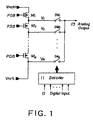
- Fig. 1 is a circuit diagram that shows a DA converter taken as the first embodiment of the invention, which is of a resistor-string type using N pieces of MOS transistors M1 ⁇ MN in series.
- MOS transistors M1 ⁇ MN have gates supplied with a voltage to activate them in a linear region, and are adjusted to have a specific ON resistance value. In this case, it is important that all of the MOS transistors are uniform in ON resistance value than in absolute value of the ON resistance value. This can be easily controlled because all MOS transistors are arranged on a common chip.
- MOS transistors M1 ⁇ MN have the function of dividing a voltage between a high potential reference voltage VrefH and a low potential reference voltage VrefL and generating analog voltages V1 ⁇ VN.
- Each of the MOS transistors M1 ⁇ MN also has the function of a switch for preventing a flow or a current from the high potential reference voltage VrefH to the low potential reference voltage VrefL and thereby preventing useless consumption of the power while the DA converter is in rest.
- a power-down signal PDB maintains the drain current of all MOS transistors M1 ⁇ MN substantially zero and prevents consumption of the current.
- a digital input 12 is converted by a decoder 11 to a selection signal corresponding to the digital data, and one of switches SW1 through SWN associated with analog voltages V1 ⁇ VN is selected. As a result, one of analog voltages V1 ⁇ VN is selected and output as the analog output 13.
- Switches SW1 ⁇ SWN can be realized by using MOS transistors.
- the full scale voltage of the DA converter is (VrefH-VrefL) x Rr x N/(Rr x N) and it is constant regardless of the value Rr of the ON resistance. Even when the manufacturing fluctuation among integrated circuits is taken into consideration, since it is not difficult to uniform the MOS transistors in property to be substantially equal in ON resistance, the full scale voltage remains constant.
- the configuration according to the first embodiment can maintain the full scale voltage affecting the accuracy of the DA converter constant without reducing the ON resistance of the MOS transistors, and therefore increases the accuracy of the analog voltage value output 13.
- the first embodiment has been explained as turning off all MOS transistors during inactivation of the DA converter by giving the power-down signal PDB to all MOS transistors M1 ⁇ MN, the current can be blocked also by giving the power-down signal PDB to only one of the MOS transistors, and the same effect will be obtained.
- the first embodiment since the first embodiment employs MOS transistors M1 ⁇ MN having specific resistance values in a linear region as voltage-dividing resistors arranged in series between the high potential reference voltage VrefH and the low potential reference voltage VrefL, it can make all or part of the MOS transistors function to cut the current during the power-down period of the DA converter, which enables omission of power-down MOS transistors heretofore indispensable for realizing a low ON resistance value and having occupied a significant part of the chip area. Therefore, the embodiment is effective for reducing the number of elements and reducing the chip area.
- the embodiment can alleviate factors of increasing the chip area toward improvement of frequency.
- any MOS transistor M1 ⁇ MN located at a desired position can be used.
- one of, or any number of, transistors M1 ⁇ MN can be used. In this manner, the cutting will be more reliable regardless of the magnitude of the potential difference between the high voltage side power source and the low voltage side power source. That is, in case the series of transistors are made up of Nch type MOS transistors, one close to the high voltage side may be used for cutting. In case they are made up of Pch type MOS transistors, one close to the low voltage side may be used for cutting. Thus a reliable cutting effect is expected.
- a plurality of transistors are used for cutting instead of using only one, the cutting effect can be made substantially perfect.
- the circuit of Fig. 1 is incorporated into another circuit, it is important whichever position one or more transistors for cutting are selected, from the viewpoints of minimizing the wirings, saving the space, minimizing the parasitic capacitance, and so on. Since any transistor in any position is usable for cutting in the circuit of Fig. 1, this circuit is useful from those viewpoints. This advantage is similarly given also by the circuits of Figs. 2 and 3, which will be explained below.
- Fig. 2 is a circuit diagram of a DA converter taken as the second embodiment of the invention, which has a configuration dividing the digital input signal to higher-order bits and lower-order bits and combining two DA converter blocks, one for the higher-order bits and the other for the lower-order bits.
- resistors RM1 ⁇ RMN have the function of dividing a voltage between a high potential reference voltage VrefH and a low potential reference voltage VrefL and generating analog voltages V1 ⁇ VN.
- a MOS transistor M1 plays the role as a switch for preventing a flow of a current from the high potential reference voltage VrefH to the low potential reference voltage VrefL and thereby preventing useless consumption of the power while the DA converter is in rest. That is, when the DA converter is in rest, a power-down signal PDB maintains the drain current of the MOS transistor M1 substantially zero, and prevents consumption of the current.
- MOS transistors MA1 ⁇ MAN-1 Connected to higher-potential terminals of the respective resistors RM1 ⁇ RMN are MOS transistors MA1 ⁇ MAN-1 that are selectively turned ON by selection signals Vg1 ⁇ VgN-1, and their drain output is used as a secondary high potential reference voltage VH.
- MOS transistors MB1 ⁇ MBN-1 that are selectively turned ON by selection signals Vg1 ⁇ VgN-1, and their drain output is used as a secondary low potential reference voltage VL.
- a digital input 23 to the block of higher-order bits is converted to a selection signal Vg1 ⁇ VgN-1 corresponding to the digital data by a decoder 21, and it is given to MOS transistors MA1 ⁇ MAN-1 and MOS transistors MB1 ⁇ MBN-1. As a result, a corresponding MOS transistor is turned ON. Accordingly, the higher-potential voltage of one of the resistors RM2 ⁇ RMN is selected and output as the secondary high potential reference voltage VH whereas the lower-potential voltage thereof is selected and output as the secondary low potential reference voltage VL.
- MOS transistors ML2 ⁇ MLM-1 have the function of dividing a voltage between the secondary high potential reference voltage VH and the secondary low potential reference voltage VL and generating analog voltages VL1 ⁇ VLM-1. Gates of the respective MOS transistors ML2 ⁇ MLM-1 are supplied with control voltages VgL2 ⁇ VgLM-1 having them operate in a linear region.
- a digital input 24 to the block of lower-order bits is converted to a selection signal corresponding to the digital data by a decoder 22, and one of switches SW1 ⁇ SWM-1 associated with respective analog voltages VL1 ⁇ VLM-1 is selected.
- switches SW1 ⁇ SWM-1 can be realized by using MOS transistors.
- the DA converter having the configuration of Fig. 2 selects a voltage range that is data of higher-order bits, and selects an analog voltage value made by further dividing the selected voltage range with data of lower-order bits, such that it is output to the analog output 25.
- both the MOS transistors MA1 ⁇ MAN-1 and the MOS transistors MB1 ⁇ MBN-1 controlled by control signals Vg1 ⁇ VgN-1 are designed to operate in a linear region, that is, to turn ON with a certain resistance value. Therefore, the circuit needs no MOS transistor corresponding to the switch, which was conventionally provided in association with the secondary high potential reference voltage VH or secondary low potential reference voltage VL, and can save the chip area.
- MOS transistors ML2 ⁇ MLM-1 are operated in a linear region.
- the switch SWM-1 is turned ON, and at least one of MOS transistors ML2 ⁇ MLM-1 is turned OFF. In this manner, a desired analog output voltage V2 ⁇ VN can be obtained.
- the circuit according to the second embodiment since the voltage applied to the circuit for dividing the voltage with the ON resistance of the MOS transistor is relatively small, the full scale voltage of the block of lower-order bits always becomes smaller than the full scale voltage of the DA converter. As a result, the circuit can decrease voltage differences between gates and the sources of MOS transistors ML2 ⁇ MLM-1, MOS transistors MA1 ⁇ MAN-1 and MOS transistors MB1 ⁇ MBN-1.
- this embodiment can diminish the MOS transistors MA1 ⁇ MAN-1 and MOS transistors MB1 ⁇ MBN-1 in size, which were inevitably large-scaled in conventional techniques. Therefore, it is possible to reduce the chip area while maintaining a high accuracy as a DA converter.
- resistors RM1 ⁇ RMN and power-down MOS transistor M1 remain untouched.
- the chip area can be further reduced by replacing the resistors with MOS transistors and omitting the power-down transistor similarly to the first embodiment.
- Fig. 2 the example is shown as using the first stage as the set of resistors and using the second stage as the set of MOS transistors. Instead, however, any number of stages may be provided as sets of voltage-dividing transistors, and they may be connected in series.
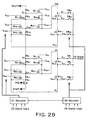
- a DA converter unit providing a resistance unit of resistances RM1-RMN, connected between the high and low potential reference voltages, is explained.
- a structure that a plurality of DA converter units are connected in series between the high and low potential reference voltages. Examples of this case are shown in Figs. 2A and 2B.
- MOS transistors MCi connected to resistance RCi of the high potential reference voltage VrefH side are P-channel type MOS transistors.
- Other points of Fig. 2B are substantially similar to Fig. 2A.
- DA converters of Figs. 2A and 2B two resistance units are provided. Therefore, it is possible that two independent MOS transistor switch groups are employed in upper and lower resistance units. For example, it is possible that threshold values, sizes and driving abilities and so on of the upper and lower switch groups are set at different values independently. Herewith a flexibility of design increases to easily construct systems according to various requirements. Furthermore, in Fig. 2B, P and N channel types MOS transistors are used. As a result, it is possible to efficiently use the voltage between the high and low potential reference voltages.
- Fig. 3 is a circuit diagram of a DA converter taken as the third embodiment of the invention, which has a R-2-R type configuration.
- this DA converter is so configured that serial MOS transistors MF0, ME1 ⁇ MEN-1 supplied with a gate control voltage VgE operate in a linear region and MOS transistors MF1 ⁇ MFN, MF1B ⁇ MFNB controlled by digital inputs 31 operate in a linear region when turned ON.
- MOS transistors MF1 ⁇ MFN are controlled by signals VgF1 ⁇ VgFN corresponding to the digital inputs 31.
- MOS transistors MF1B ⁇ MFNB are controlled by signals VgF1B ⁇ VgFNB that are inversion signals of signals VgF1 ⁇ VgFN. That is, MOS transistors MF1 ⁇ MFN and MOS transistors MF1B ⁇ MFNB are so controlled that, while one is ON, the other is OFF, or while one is OFF, the other is ON, in each of associated pairs thereof.
- MOS transistors MF1 ⁇ MFN are connected to a high potential reference voltage VrefH whereas MOS transistors MF1B ⁇ MFNB are connected to a low potential reference voltage VrefL.
- the high potential reference voltage VrefH or the low potential reference voltage VrefL is supplied to a connection point of serially connected MOS transistors MF0, ME1 ⁇ MEN-1 with the ON resistance thereof.
- the embodiment since the characteristics are determined solely by ratios of ON resistance values of all MOS transistors, it is not necessary to use large-scaled MOS transistors and thereby reduce the ON resistance values.
- all MOS transistors controlled by the digital inputs 31 function as switches and resistors, the embodiment can reduce the number of elements as compared with conventional techniques, and it is effective for reducing the total chip area.
- the embodiment makes it possible to make up the circuit with MOS transistors equal in property, it is effective also for improving the accuracy as the DA converter.
- the set of resistors and switching elements conventionally made up of combinations of resistors and MOS transistors are wholly or partly replaced by transistors operative in a linear region, their properties can be equalized relatively easily in the integrated circuit process, and accuracy can be ensured without using large-scaled transistors having small ON resistance values. Additionally, by making the best use of functions of transistors as switches and as resistors, functions of a switching element and a resistive element conventionally provided separately can be put together into a single transistor, and this is effective for reducing the number of elements and the chip area.
- the voltage-dividing resistors are made up of MOS transistors, these transistors can be used also to cut off the high voltage side potential and the low voltage side potential as voltage-dividing potentials from each other.
- the transistor may be any in any position of the set of the transistors, a transistor minimizing the length of wiring can be used for cutting when making and connecting wirings for applying a shut-off controlling signal.
- it is possible not only to increase the margin for circuit design but also to decrease the parasitic capacitance, or the like, to improve the property.
- any desired number of transistors may be used for cutting to ensure more reliable cutting.
Landscapes
- Engineering & Computer Science (AREA)
- Theoretical Computer Science (AREA)
- Analogue/Digital Conversion (AREA)
Abstract
Description
Claims (23)
- A DA converter for dividing a reference voltage and outputting a partial voltage corresponding to an input digital data, comprising:a set of resistive elements connected to said reference voltage and made up of serially connected resistive elements which are made of transistors, any number of said transistors at any position being usable for cutting the circuit off; anda partial voltage extracting circuit for having a partial voltage corresponding to said input digital data be output from said set of resistive elements.
- A DA converter according to claim 1 wherein said transistors are arranged on a common chip.
- The DA converter according to claim 1 wherein said transistors are MOS transistors having a specific resistance value at the ON state.
- A DA converter according to claim 3 wherein each said transistor is an N-channel type transistor, and any number of said transistors at higher voltage sides are used for cutting the circuit off.
- A DA converter according to claim 3 wherein each said transistor is a P-channel type transistor and any number of said transistors at lower voltage sides are used for cutting the circuit off.
- A DA converter according to claim 1 wherein said partial voltage extracting circuit includes a plurality of switches each connected to one end of each said transistor, and one of said switches is closed depending on said input digital data such that said partial voltage is output.
- A DA converter according to claim 6 wherein said switch is a MOS transistor.
- A DA converter for dividing a reference voltage and outputting a partial voltage corresponding to an input digital data, comprising:a first set of resistive elements connected to said reference voltage, having a plurality of serially connected first resistive elements;a first partial voltage extracting circuit for outputting a first partial voltage corresponding to one part of said input digital data be output from said first set of resistive elements;a second set of resistive elements connected to said first partial voltage and having a plurality of serially connected second resistive elements; anda second partial voltage extracting circuit for outputting a second partial voltage corresponding to the other part of said input digital data be output from said second set of resistive elements.
- A DA converter according to claim 8 wherein said first partial voltage extracting circuit includes a plurality of first partial voltage switches each connected to one end of any one of said first resistive elements, and one of said first partial voltage switches is closed depending on one part of said input digital data such that said first partial voltage is output, the other ends of said first partial switches being commonly connected to one end of said second set of resistive elements.
- A DA converter according to claim 9 wherein said first partial voltage switches are MOS transistors.
- A DA converter according to claim 9 wherein said first partial voltage extracting circuit further includes a plurality of first switches, one end of each first switch being commonly connected to said other end of said second set of resistive elements, the other end of each said first switch being connected to one end of predetermined one of said first resistive elements in said first set of resistive elements, said first switches being selectively controlled conductive by one part of said input digital data.
- A DA converter according to claim 8 wherein said second partial voltage extracting circuit includes second partial voltage switches each connected to one end of any one of said second resistive elements, and one of said second partial voltage switches is closed depending on the other part of said input digital data such that said second partial voltage is output.
- A DA converter according to claim 12 wherein said first partial voltage switches, said first switches and second resistive elements are MOS transistors arranged on a common chip.
- A DA converter according to claim 13 wherein said second partial voltage switches are MOS transistors.
- ADA converter according to claim 13 wherein said first partial voltage switches, said first switches and second resistive elements are MOS transistors having a specific resistance value at the ON state.
- A DA converter according to claim 15 wherein each said transistor is an N-channel type transistor, and any number of said transistors at higher voltage sides are used for cutting the circuit off.
- A DA converter according to claim 15 wherein each said transistor is a P-channel type transistor, and any number of said transistors at lower voltage sides are used for cutting the circuit off.
- A DA converter for outputting a reference voltage as a partial voltage corresponding to an input digital data from an output end, comprising:a first set of resistor elements including a plurality of resistive elements connected in series between a first reference voltage and said output end;a first set of transistors including a plurality of first transistors each functioning as a switch and as a resistive element in the ON state thereof, each said first transistor being connected at one end to said first reference voltage and at the other end to one end of predetermined one of said resistive elements; anda second set of transistors including a plurality of second transistors each functioning as a switch and as a resistive element in the ON state thereof, each said second transistor being connected at one end to said second reference voltage and at the other end to the other end of associated one of said first transistors, each said first transistor and associated one of said second transistors being controlled such that one of them turns ON whereas the other turns OFF, depending on said digital input.
- A DA converter according to claim 18 wherein resistance value of each said resistive element and ON resistance of each said first transistor are equally adjusted to a first resistance value, and each said second transistor has a second resistance value, said first resistance value being adjusted to approximately one half of said second resistance value.
- A DA converter according to claim 18 wherein said resistive elements, said first transistors and said second transistors are MOS transistors and arranged on a common chip.
- A DA converter for dividing a reference voltage and outputting a partial voltage corresponding to an input digital data providing a plurality of DA converter units serially connected to said reference voltage, each said DA converter, comprising:a first set of resistive elements connected to said reference voltage and having a plurality of serially connected first resistive elements;a first partial voltage extracting circuit for having a first partial voltage corresponding to one part of said input digital data be output from said first set of resistive elements;a second set of resistive elements connected to said first partial voltage and having a plurality of serially connected second resistance elements; anda second partial voltage extracting circuit for having a second partial voltage corresponding to the other part of said input digital data be output from said second set of resistive elements.
- A DA converter according to claim 21 wherein said first partial voltage extracting circuit and second set of resistive elements include MOS transistors, said MOS transistors of DA converter units are same channel type transistors.
- A DA converter according to claim 21 wherein said first partial voltage extracting circuit and second set of resistive elements include MOS transistors, said MOS transistors of one of DA converter units and said MOS transistors of another of DA converter units are different channel type transistors.
Applications Claiming Priority (2)
| Application Number | Priority Date | Filing Date | Title |
|---|---|---|---|
| JP2000259232 | 2000-08-29 | ||
| JP2000259232A JP2002076897A (en) | 2000-08-29 | 2000-08-29 | DA converter |
Publications (2)
| Publication Number | Publication Date |
|---|---|
| EP1184989A2 true EP1184989A2 (en) | 2002-03-06 |
| EP1184989A3 EP1184989A3 (en) | 2004-07-21 |
Family
ID=18747431
Family Applications (1)
| Application Number | Title | Priority Date | Filing Date |
|---|---|---|---|
| EP01120619A Withdrawn EP1184989A3 (en) | 2000-08-29 | 2001-08-29 | DA converter |
Country Status (3)
| Country | Link |
|---|---|
| US (1) | US6570520B2 (en) |
| EP (1) | EP1184989A3 (en) |
| JP (1) | JP2002076897A (en) |
Cited By (3)
| Publication number | Priority date | Publication date | Assignee | Title |
|---|---|---|---|---|
| WO2006053157A1 (en) * | 2004-11-12 | 2006-05-18 | Analog Devices, Inc. | Balanced dual resistor string digital to analog converter system and method |
| EP1903684A1 (en) * | 2006-09-22 | 2008-03-26 | Samsung SDI Co., Ltd. | Driving circuit and organic light emitting diode display device thereof |
| WO2008026067A3 (en) * | 2006-08-31 | 2008-05-22 | Ati Technologies Ulc | Reduced component digital to analog decoder and method |
Families Citing this family (18)
| Publication number | Priority date | Publication date | Assignee | Title |
|---|---|---|---|---|
| US20030203451A1 (en) * | 2000-08-24 | 2003-10-30 | Genentech, Inc. | IL-17 homologous polypeptides and therapeutic uses thereof |
| JP4397291B2 (en) * | 2004-06-29 | 2010-01-13 | Okiセミコンダクタ株式会社 | Display device drive circuit and display device drive method |
| JP4751122B2 (en) * | 2005-07-28 | 2011-08-17 | 株式会社東芝 | A / D converter |
| JP4625739B2 (en) * | 2005-09-05 | 2011-02-02 | 株式会社東芝 | Resistor voltage division type digital / analog conversion circuit |
| KR100671648B1 (en) * | 2005-12-08 | 2007-01-19 | 삼성에스디아이 주식회사 | Data driver, organic light emitting display using same and driving method thereof |
| US7372387B2 (en) * | 2006-09-01 | 2008-05-13 | Texas Instruments Incorporated | Digital-to-analog converter with triode region transistors in resistor/switch network |
| KR100815754B1 (en) * | 2006-11-09 | 2008-03-20 | 삼성에스디아이 주식회사 | Driving circuit and organic light emitting display device using same |
| US8344790B2 (en) * | 2007-11-21 | 2013-01-01 | O2Micro Inc. | Circuits and methods for controlling a charge pump system |
| US9118238B2 (en) * | 2007-11-21 | 2015-08-25 | O2Micro, Inc. | Charge pump systems with adjustable frequency control |
| US7868809B2 (en) * | 2007-12-21 | 2011-01-11 | International Business Machines Corporation | Digital to analog converter having fastpaths |
| CA2721713C (en) * | 2008-05-05 | 2019-07-09 | Novimmune Sa | Anti-il-17a/il-17f cross-reactive antibodies and methods of use thereof |
| JP5193003B2 (en) * | 2008-12-02 | 2013-05-08 | シャープ株式会社 | LED driving device and LED driving control method |
| EP2427203B1 (en) * | 2009-05-05 | 2018-10-17 | Novimmune S.A. | Anti-il-17f antibodies and use thereof |
| US8269659B2 (en) * | 2010-10-15 | 2012-09-18 | Stmicroelectronics Asia Pacific Pte., Ltd. | System and method for compact cyclic digital to analog converter |
| JP5559823B2 (en) * | 2012-01-18 | 2014-07-23 | 東京エレクトロン株式会社 | Digital / analog converter |
| KR101985502B1 (en) | 2012-07-04 | 2019-06-04 | 삼성디스플레이 주식회사 | Display device, control device for driving the display device, and drive control method thereof |
| JP7353512B2 (en) * | 2020-10-05 | 2023-09-29 | 三菱電機株式会社 | digital analog converter |
| EP4589594A1 (en) | 2022-09-16 | 2025-07-23 | Kioxia Corporation | Semiconductor device and memory device |
Family Cites Families (4)
| Publication number | Priority date | Publication date | Assignee | Title |
|---|---|---|---|---|
| US5731775A (en) * | 1996-06-17 | 1998-03-24 | Lucent Technologies Inc. | Subranging converter with plurality of resistor strings and transistor switches |
| IT1289207B1 (en) * | 1996-10-24 | 1998-09-29 | Sgs Thomson Microelectronics | COMPENSATED MOS-RESISTIVE POTENTIOMETRIC STRING AND DIGITAL / ANALOG CONVERTER USING THIS STRING |
| US5969657A (en) * | 1997-07-22 | 1999-10-19 | Analog Devices, Inc. | Digital to analog converter |
| US5977898A (en) * | 1997-12-22 | 1999-11-02 | Texas Instruments Incorporated | Decoding scheme for a dual resistor string DAC |
-
2000
- 2000-08-29 JP JP2000259232A patent/JP2002076897A/en active Pending
-
2001
- 2001-08-29 US US09/942,433 patent/US6570520B2/en not_active Expired - Fee Related
- 2001-08-29 EP EP01120619A patent/EP1184989A3/en not_active Withdrawn
Cited By (7)
| Publication number | Priority date | Publication date | Assignee | Title |
|---|---|---|---|---|
| WO2006053157A1 (en) * | 2004-11-12 | 2006-05-18 | Analog Devices, Inc. | Balanced dual resistor string digital to analog converter system and method |
| US7259706B2 (en) | 2004-11-12 | 2007-08-21 | Analog Devices, Inc. | Balanced dual resistor string digital to analog converter system and method |
| CN101057407B (en) * | 2004-11-12 | 2011-08-10 | 联发科技股份有限公司 | Balanced two-resistor string digital-to-analog converter system and method |
| WO2008026067A3 (en) * | 2006-08-31 | 2008-05-22 | Ati Technologies Ulc | Reduced component digital to analog decoder and method |
| US8031093B2 (en) | 2006-08-31 | 2011-10-04 | Ati Technologies Ulc | Reduced component digital to analog decoder and method |
| CN101523730B (en) * | 2006-08-31 | 2013-09-18 | Ati科技无限责任公司 | Reduced component digital to analog decoder and method |
| EP1903684A1 (en) * | 2006-09-22 | 2008-03-26 | Samsung SDI Co., Ltd. | Driving circuit and organic light emitting diode display device thereof |
Also Published As
| Publication number | Publication date |
|---|---|
| EP1184989A3 (en) | 2004-07-21 |
| JP2002076897A (en) | 2002-03-15 |
| US20020047791A1 (en) | 2002-04-25 |
| US6570520B2 (en) | 2003-05-27 |
Similar Documents
| Publication | Publication Date | Title |
|---|---|---|
| US6570520B2 (en) | DA converter | |
| JP4546539B2 (en) | Current addition type DAC | |
| US5999115A (en) | Segmented DAC using PMOS and NMOS switches for improved span | |
| US9100045B2 (en) | Multiple string digital to analog converter | |
| US6222473B1 (en) | Method and apparatus for digital to analog converters with improved switched R-2R ladders | |
| US6201491B1 (en) | Digitally switched potentiometer having improved linearity and settling time | |
| US12445139B2 (en) | DAC with configurable output stage | |
| JP4358450B2 (en) | Method and apparatus for switching a low voltage CMOS switch in a high voltage digital / analog converter | |
| US7323923B2 (en) | Driver circuit | |
| US8587358B2 (en) | Semiconductor integrated circuit including variable resistor circuit | |
| US10511321B2 (en) | Digital-to-analog converter and method for digital-to-analog conversion | |
| EP2782256B1 (en) | A digital to analogue converter | |
| JPH04268825A (en) | Digital to analog converter | |
| JPH11251914A5 (en) | Voltage selection circuit, LCD driver circuit and D/A converter | |
| KR20020059803A (en) | Digital-to-analog converter | |
| US5936563A (en) | Digital-to-analog conversion circuit | |
| EP3182243A1 (en) | Active potentiometer circuit | |
| US6150971A (en) | R/2R' ladder switch circuit and method for digital-to-analog converter | |
| US6784651B2 (en) | Current source assembly controllable in response to a control voltage | |
| US7277036B2 (en) | Digital-to-analog converting circuit | |
| JP3730713B2 (en) | Digital / analog converter | |
| JPS6387809A (en) | Operational amplifier | |
| KR20010042440A (en) | A current compensating bias generator and method therefor | |
| KR20040033744A (en) | Variable voltage dividing circuit | |
| JP2001144618A (en) | Digital/analog converter |
Legal Events
| Date | Code | Title | Description |
|---|---|---|---|
| PUAI | Public reference made under article 153(3) epc to a published international application that has entered the european phase |
Free format text: ORIGINAL CODE: 0009012 |
|
| 17P | Request for examination filed |
Effective date: 20010829 |
|
| AK | Designated contracting states |
Kind code of ref document: A2 Designated state(s): AT BE CH CY DE DK ES FI FR GB GR IE IT LI LU MC NL PT SE TR |
|
| AX | Request for extension of the european patent |
Free format text: AL;LT;LV;MK;RO;SI |
|
| RIN1 | Information on inventor provided before grant (corrected) |
Inventor name: ISHII, HIROTOMO |
|
| PUAL | Search report despatched |
Free format text: ORIGINAL CODE: 0009013 |
|
| AK | Designated contracting states |
Kind code of ref document: A3 Designated state(s): AT BE CH CY DE DK ES FI FR GB GR IE IT LI LU MC NL PT SE TR |
|
| AX | Request for extension of the european patent |
Extension state: AL LT LV MK RO SI |
|
| 17Q | First examination report despatched |
Effective date: 20040929 |
|
| AKX | Designation fees paid |
Designated state(s): DE FR GB |
|
| STAA | Information on the status of an ep patent application or granted ep patent |
Free format text: STATUS: THE APPLICATION IS DEEMED TO BE WITHDRAWN |
|
| 18D | Application deemed to be withdrawn |
Effective date: 20051103 |