EP1182886A2 - Filtering method and apparatus for the reduction of image blocking artifacts - Google Patents
Filtering method and apparatus for the reduction of image blocking artifacts Download PDFInfo
- Publication number
- EP1182886A2 EP1182886A2 EP01119346A EP01119346A EP1182886A2 EP 1182886 A2 EP1182886 A2 EP 1182886A2 EP 01119346 A EP01119346 A EP 01119346A EP 01119346 A EP01119346 A EP 01119346A EP 1182886 A2 EP1182886 A2 EP 1182886A2
- Authority
- EP
- European Patent Office
- Prior art keywords
- output
- mode operation
- group
- value
- mode
- Prior art date
- Legal status (The legal status is an assumption and is not a legal conclusion. Google has not performed a legal analysis and makes no representation as to the accuracy of the status listed.)
- Withdrawn
Links
Images



Classifications
-
- H—ELECTRICITY
- H04—ELECTRIC COMMUNICATION TECHNIQUE
- H04N—PICTORIAL COMMUNICATION, e.g. TELEVISION
- H04N19/00—Methods or arrangements for coding, decoding, compressing or decompressing digital video signals
- H04N19/85—Methods or arrangements for coding, decoding, compressing or decompressing digital video signals using pre-processing or post-processing specially adapted for video compression
- H04N19/86—Methods or arrangements for coding, decoding, compressing or decompressing digital video signals using pre-processing or post-processing specially adapted for video compression involving reduction of coding artifacts, e.g. of blockiness
-
- H—ELECTRICITY
- H04—ELECTRIC COMMUNICATION TECHNIQUE
- H04N—PICTORIAL COMMUNICATION, e.g. TELEVISION
- H04N19/00—Methods or arrangements for coding, decoding, compressing or decompressing digital video signals
- H04N19/50—Methods or arrangements for coding, decoding, compressing or decompressing digital video signals using predictive coding
- H04N19/503—Methods or arrangements for coding, decoding, compressing or decompressing digital video signals using predictive coding involving temporal prediction
- H04N19/51—Motion estimation or motion compensation
- H04N19/527—Global motion vector estimation
Definitions
- the present invention relates to the processing performed for a recovered image during a digital image compression process, and relates in particular to a deblocking filtering apparatus and method defined in MPEG-4.
- the internationally accepted MPEG digital image compression standards provide for the employment of a discrete cosine transform.
- This is an irreversible transform used for quantization, and depending on the condition of an original image, a phenomenon occurs whereby a pseudo outline having a block shape (block noise), which is inherent to the system, may appear in a recovered image.
- Vertification Model 7.0 of the MPEG-4 video standards defines a deblocking filter as a post process for a recovered image. As is shown in Fig. 3, the defined deblocking filter performs filtering for ten received pixel values positioned around the block boundary, and outputs eight pixel values positioned around the block boundary. Two types of operation modes, a DC offset mode operation (hereinafter referred to as a D mode operation) and a default mode operation, are switched in accordance with a change value (hereinafter referred to as an activity) for the value of a pixel near the block boundary.
- An evaluation function representing the activity employs the following equation (1).
- an absolute differential value for the difference between adjacent pixel values is compared with a threshold value Th1, and a count is acquired of the locations whereat the absolute differential value is equal to or smaller than the threshold value Th1. If the value of the evaluation function f is equal to or greater than a threshold value Th2, i.e., when the activity is low, the D mode operation is selected. But if the value of the evaluation function f is smaller than the threshold value Th2, i.e., when the activity is high, the default mode operation is selected.
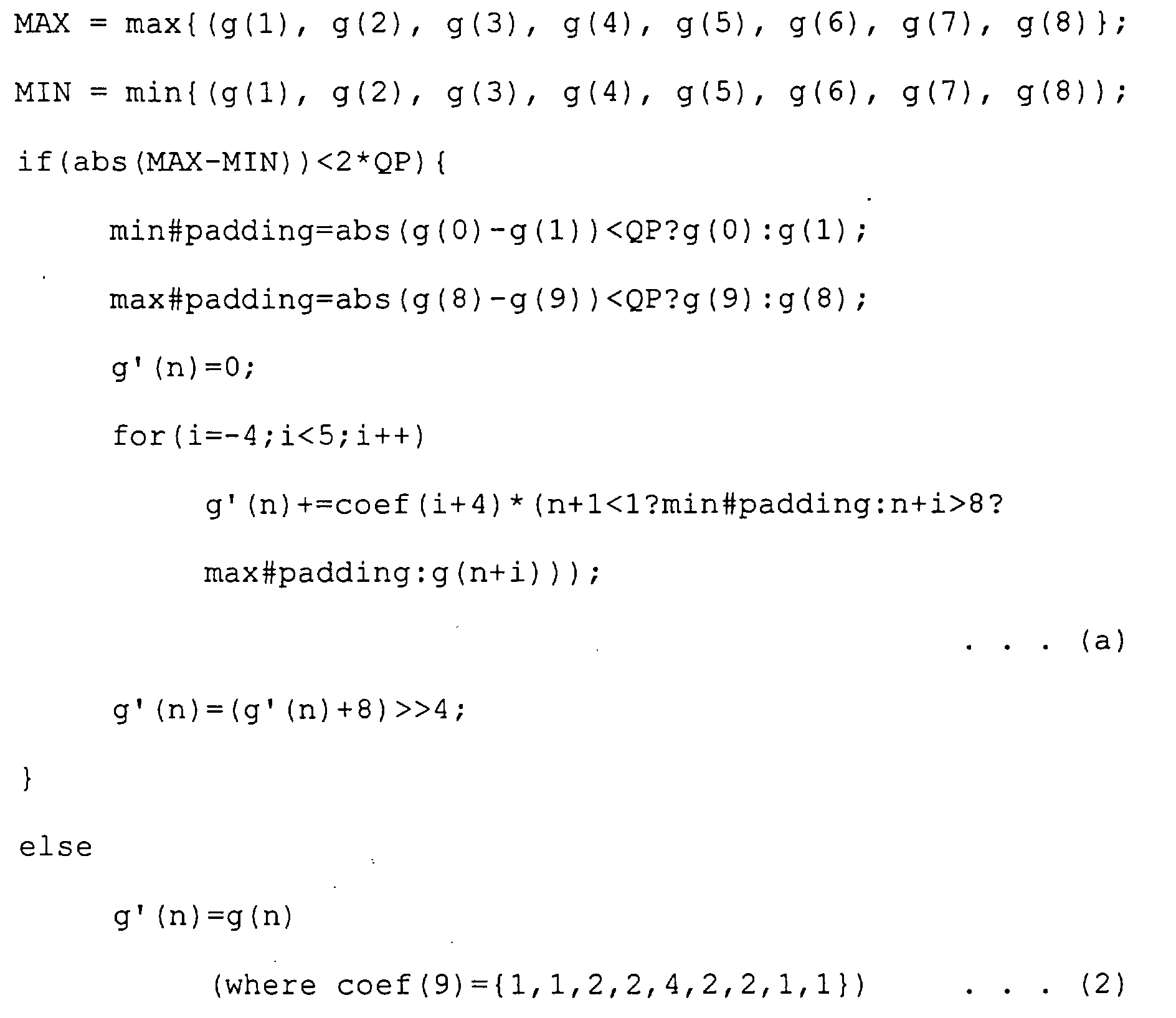
- a more effective smoothing process is performed for a D mode operation than is performed for a default mode operation, as is illustrated by an operation equation (2) that is shown below.
- the smoothing process is performed if the absolute differential value between a maximum pixel value and a minimum pixel value for a string of eight pixels positioned around a block boundary is smaller than twice a quantization parameter QP. If the absolute differential value is equal to or greater than twice the quantization parameter QP, the smoothing process is not performed and an input pixel value is output unchanged.
- Equation (3) is obtained by specially developing formula (a) in equation (2), and the smoothing process is performed by a weighting function employed mainly for a target pixel and the logical sum of the input pixel string.
- g'(1) min+min+2*min+2*min+4*g(1)+2*g(2)+2*g(3)+g(4)+g(5);
- g'(2) min+min+2*min+2*g(1)+4*g(2)+2*g(3)+2*g(4)+g(5)+g(6);
- g'(3) min+min+2*g(1)+2*g(2)+4*g(3)+2*g(4)+2*g(5)+g(6)+g(7) ;
- g'(4) min+g(1)+2*g(2)+2*g(3)+4*g(4)+2*g(5)+2*g(6)+g(7)+g(8 );
- g'(5) g(1)+g(2)+2*g(3)+2*g(4)+4*g(5)+2*g(6)+2*g(7)+g(8)
- Telenor's adaptive filtering (hereinafter referred to as a T mode operation), which has a smaller calculation amount, may be employed, as is illustrated by a T mode operation (5) that follows.
- the smoothing process is performed for only two pixels along a block boundary, and the input values of all other pixels are output unchanged.
- the evaluation function d in equation (5) is equal to or smaller than a quantization parameter QP/2
- a smoothing process is performed in which the value of the evaluation function d is added to or is subtracted from the input pixel value. Then, if the evaluation function value d is greater than the quantization parameter QP/2, the input pixel value is output unchanged.
- the above deblocking filtering defined by MPEG-4 is first performed along all horizontal edges, and is then performed along all vertical edges.
- the above deblocking filter operation is performed, using software, by a general-purpose calculator in a processor, or part of the deblocking filter operation is performed by special hardware and the remainder of the operation is performed, using software, by a general-purpose calculator in a processor.
- Fig. 4 is a block diagram showing the special hardware operation for formula (a) in the D mode operation equation (2).
- a counter 100 counts processing cycles from 0 to 7
- operation blocks 101 to 108 correspond to filtering target pixels n (n is an integer from 1 to 8)
- an output selector 109 selects one of the outputs of the operation blocks 101 to 108.
- the operation block 101 includes: first and second selectors n11 and n12, for receiving at least two of the externally input data max_padding, min_padding, input pixel values g(x) and g(x+1), and data 0; a third selector n13, for receiving data "8" and the output of a register n17, which will be described later; first and second shifters n14 and n15, for shifting the output of both the first and the second selectors n11 and n12; an adder n16 for adding the output of the first and the second shifters n14 and n15 to the output of the third selector n13; the register n17, for holding the output of the adder n16; and a third shifter n18, for shifting the output of the register n17.
- the operation blocks 102 to 108 have the same configuration as the operation block 101, and include, respectively, first selectors n21, n31, n41, n51, n61, n71 and n81; second selectors n22, n32, n42, n52, n62, n72 and n82; third selectors n23, n33, n43, n53, n63, n73 and n83; first shifters n24, n34, n44, n54, n64, n74 and n84; second shifters n25, n35, n45, n55, n65, n75 and n85; adders n26, n36, n46, n56, n66, n76 and n86; registers n27, n37, n47, n57, n67, n77 and n87; and third shifters n28, n38,
- a deblocking filtering apparatus comprises:
- the operation mode determination circuit performs a process before, in a time series, the processes for the D mode operation circuit and the T mode operation circuit; selects either the D mode operation circuit or the T mode operation circuit as an adaptive operation circuit; and transmits a fixed value, instead of an input pixel value, to a non-adaptive operation circuit.
- the D mode operation circuit includes:
- a deblocking filtering method comprises:
- the operation mode determination is performed before, in a time series, the D mode operation and the T mode operation are initiated, either the D mode operation or the T mode operation is determined as an adaptive operation, and a fixed value, rather than an input pixel value, is input as a non-adaptive operation.
- the D mode operation circuit, the T mode operation circuit and the operation mode determination circuit all of which process sequentially input pixel values, are operated in parallel and in synchronization with the input timing for the pixel value.
- all the operations can be completed within the number of process cycles for the operation circuit having the maximum process cycles. Therefore, the software process that uses the general-purpose calculator of the computer is not required, and the deblocking filtering can be performed quickly and requires only a small number of process cycles.
- the operation mode determination is performed before the D mode operation and T mode operation. Therefore, an adaptive operation can be determined in advance, and the input pixel value for a non-adaptive operation can be defined as a fixed value. Thus, both the number of calculations required and the power consumption can be reduced.
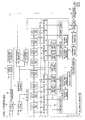
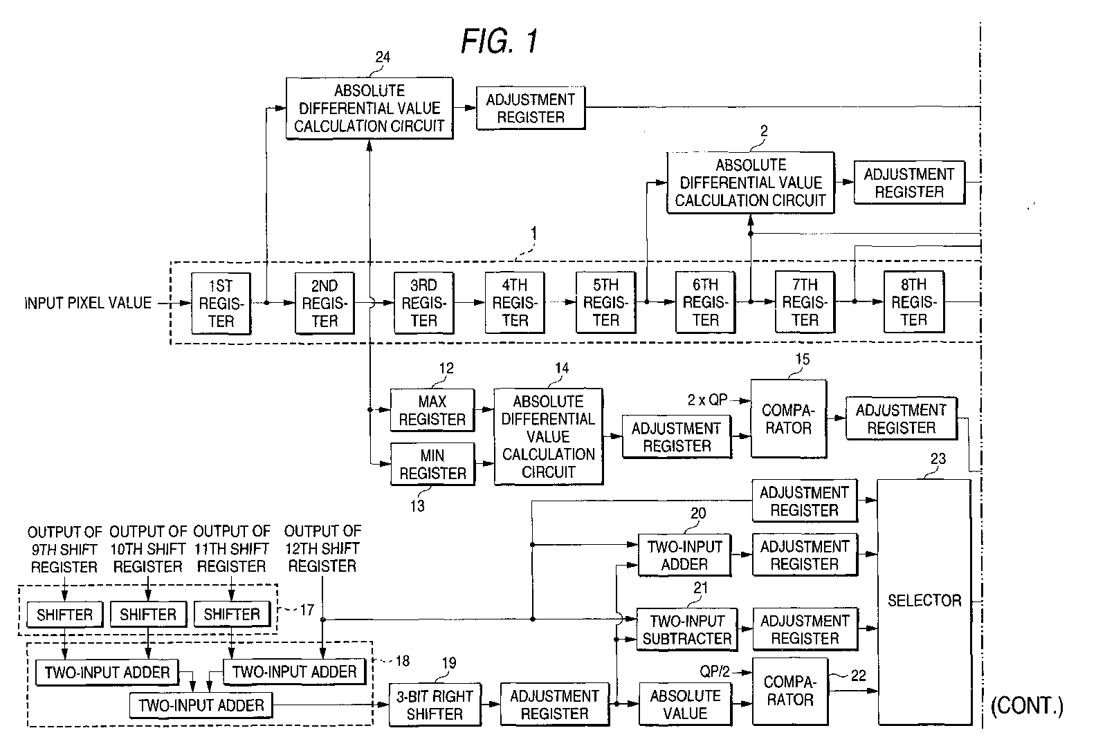
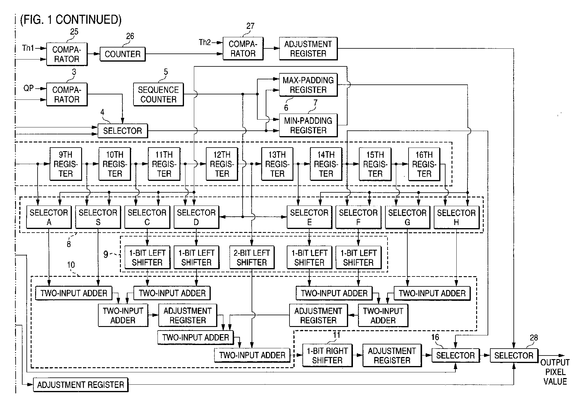
- FIG. 1 is a block diagram showing a deblocking filtering apparatus according to this embodiment.
- the deblocking filtering apparatus comprises: a shift register group 1; a first absolute differential value calculation circuit 2, for calculating the absolute differential value for a difference between specific adjacent registers in the shift register group 1; a first comparator 3, for comparing the output of the first absolute differential calculation circuit 2 with a quantization parameter QP (first threshold value); a first selector 4, for employing the output of the first comparator 3 to select one of the register values to be input to the first absolute differential calculation circuit 2; a sequence counter 5; and first and second register values 6 and 7, for holding the output of the first selector 4 during a specific sequence cycle indicated by the count value of the sequence counter 5.
- the deblocking filtering apparatus comprises: a selector group 8, for switching the output of the shift register group 1 and the output of the first and of the second registers in accordance with the output of the sequence counter 5; a first shifter group 9, for shifting the output of the selector group 8 one bit or two bits to the left; a first, two-input adder group 10, for adding the output of the selector group 8 to the output of the first shifter group 9; and a first shifter 11, for shifting the output of the two-input adder group 10 four bits to the right.
- the deblocking filtering apparatus also comprises: a third register 12, for holding the maximum value for a specific register output by the shift register group 1; a fourth register 13, for holding the minimum value for a specific register output by the shift register group 1; a second absolute differential value calculation circuit 14, for obtaining the absolute differential value for a difference between the third register output and the fourth register output; a second comparator 15, for comparing the output of the second absolute differential value calculation circuit 14 with a value (second threshold value) that is twice that of the quantization parameter QP; and a second selector 16, for switching the output of the specific register in the shift register group 1 and the output of the first shifter 11 in accordance with the results of the second comparator 15.
- the components 1 to 16 constitute an operation block for the D mode operation.
- the deblocking filtering apparatus additionally comprises: a second shifter group 17; a second two-input adder group 18, for adding the output of a specific register in the shift register group 1 to the output of the second shifter group 17; a second shifter 19, for shifting the output of the second two-input adder group 18 three bits to the right; a two-input adder 20, for adding the output of the second shifter 19 to the output of the specific register in the shift register group 1; a two-input subtracter 21, for subtracting the output of the second shifter 19 from the output of the specific register in the shift register group 1; a third comparator 22, for comparing the output of the second shifter 19 with a quantization parameter QP/2 (third threshold value); and a third selector 23, for switching the output of a specific register in the shift register group 1, the output of the two-input adder 20 and the output of the two-input subtracter 21 in accordance with the output of the third comparator 22.
- the components 17 to 23 constitute an operation block for the T
- the deblocking filtering apparatus in Fig. 1 comprises: a third absolute differential value calculation circuit 24, for calculating the absolute differential value for a difference between specific adjacent registers in the shift register group 1; a fourth comparator 25, for comparing the output of the third absolute differential calculation circuit 24 with a threshold value Th1 (fourth threshold value); a counter 26, for cumulatively adding the output of the fourth comparator 25; a fifth comparator 27, for comparing the output of the counter 26 with a threshold value Th2 (fifth threshold value); and a fourth selector 28, for switching the output of the second selector 16 with the output of the third selector 23 in accordance with the output of the fifth comparator 27.
- the components 24 to 28 form an operation mode determination circuit block for determining whether a D mode operation or a T mode operation should be selected.
- a timing adjustment register is provided as needed in the circuit in order to adjust the number of operation cycles that differ in the processing paths.
- Ten pixel values positioned along the block boundary, a(0), a(1), a(2), a(3), a(4), a(5), a(6), a(7), a(8) and a(9), are arranged in order, beginning with a(0) on the left; and ten pixel values positioned along the block boundary of the next line, b(0), b(1), b(2), b(3), b(4), b(5), b(6), b(7), b(8) and b(9), are arranged in order, beginning with b(0) on the left.
- Pixel value data is transmitted to the shift register group 1 each cycle in the order a(0), a(1) and a(2), and when the cycle for transmitting a(0) is defined as cycle 0, at cycle 1, a(0) serves as the output of the first register of the shift register group 1, and at cycle 2, a(0) serves as the output of the second register.
- the first absolute differential value calculation circuit 2 calculates the absolute differential value for the difference between a(0) and a(1).
- the first comparator 3 compares the absolute differential value with the quantization parameter QP. Then, if as the result of a comparison it is found that the absolute differential value is smaller than the quantization parameter QP, the first selector 4 selects a(0), which is the output of the eighth register in the shift register group 1. However, if the absolute differential value is found to be equal to or greater than the quantization parameter QP, the first selector 4 selects a(1), which is the output of the seventh register in the shift register group 1.
- the first register 6 holds the output of the first selector 4.
- the value held by the first register 6 is min_padding value in equation (2).
- the first absolute differential value calculation circuit 2 calculates the absolute value for the difference between a (8) and a(9).
- the first comparator 3 compares the obtained absolute differential value with the quantization parameter QP. Then, if as the result of a comparison it is found that the absolute differential value is smaller than the quantization parameter QP, the first selector 4 selects a(9), which is the output of the seventh register in the shift register group 1. However, if the output of the absolute differential value is found to be equal to or greater than the quantization parameter QP, the eighth register output, a(8), is selected.
- the second register 7 holds the output of the first selector 4. The value held by the second register 7 is the max_padding value in equation (2).
- a smoothing process is performed by using the 8-th to the 16-th register outputs of the shift register 1, and the min_padding value and the max_padding value.
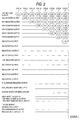
- Each selector in the selector group 8 is operated in the following manner during a period extending from cycle 13 to cycle 20.
- the selector A outputs the value of the eighth register in the shift register group 1 during a period extending from cycle 13 to cycle 16, and outputs the max_padding value during a period extending from cycle 17 to cycle 20.
- the selector B outputs the value of the ninth register in the shift register group 1 during a period extending from cycle 13 to cycle 17, and outputs the max_padding value during a period extending from cycle 18 to cycle 20.
- the selector C outputs the value of the tenth register in the shift register group 1 during a period extending from cycle 13 to cycle 18, and outputs the max_padding value during a period extending from cycle 19 to cycle 20.
- the selector D outputs the value of the eleventh register in the shift register group 1 during a period extending from cycle 13 to cycle 19, and outputs the max_padding value at cycle 20.
- the selector E outputs the min_padding value at cycle 13, and outputs the value of the thirteenth register during a period extending from cycle 14 to cycle 20.
- the selector F outputs the min_padding value during a period extending from cycle 13 to cycle 14, and outputs the value of the fourteenth register during a period extending from cycle 15 to cycle 20.
- the selector G outputs the min_padding value during a period extending from cycle 13 to cycle 15, and outputs the value of the fifteenth register during a period extending from cycle 16 to cycle 20.
- the selector H outputs the min_padding value during a period extending from cycle 13 to cycle 16, and outputs the value of the sixteenth register during a period extending from cycle 17 to cycle 20.
- the first shifter group 9 shifts the output of each of the selectors C to F in the selector group 8 one bit to the left, and shifts the output of the twelfth register of the shift register group 1 two bits to the left.
- the first two-input adder group 10 sums the output of the selectors A, B, G and H of the selector group 8 and the output of the shifters of the first shifter group 9, and to this adds a constant "8".
- the second shifter 11 shifts the results four bits to the right, and obtains the pixel value at the completion of the smoothing process.
- the following operation is performed to determine whether, as the output of the D mode operation, the pixel value obtained at the completion of the smoothing process should be output, or whether the input pixel value should be output unchanged.
- each cycle of the second shift register in the shift register group 1 is compared during a period extending from cycle 3 to cycle 10, and the maximum value of the input pixel values a(1) to a(8) is held in the third register 12 and the minimum value of the input pixel values a(1) to a(8) is held in the fourth register 13.
- the second absolute differential value calculation circuit 14 calculates the absolute differential value for the difference between the values held in the third register 12 and the fourth register 13.
- the second comparator 15 compares the absolute differential value with twice the quantization parameter QP.
- the second selector 16 selects the pixel value obtained at the completion of the smoothing process, which is the output of the first shifter 11. Whereas if the output of the second absolute differential value calculation circuit 14 is equal to or greater than the quantization parameter QP, the second selector 16 selects the input pixel value that is the output of fourteenth register in the shift register group 1.
- the output of the D mode operation is obtained through the above processing.
- the second shifter group 17 shifts the output of the tenth and of the eleventh shift registers in the shift register group 1 one bit to the left.
- the second two-input adder group 18 and the second shifter 19 calculate value "d" in equation (5) by using the output of the second shifter group 17 and the output of the ninth and of the twelfth shift registers of the shift register group 1.
- the two-input adder 20 adds a(4), which is the output of the twelfth shift register in the shift register group 1, to the value d in equation (5), which is the output of the second shifter 19.
- the two-input subtracter 21 subtracts the value d in equation (5), which is the output of the second shifter 19, from a(5), which is the output of the twelfth shift register in the shift register group 1. As a result, the pixel value at the completion of the smoothing process is obtained.
- the following operation is performed to determine whether, as the output of the T mode operation, the pixel value obtained at the completion of the smoothing process should be output, or whether the input pixel value should be output unchanged.
- the third comparator 22 compares the quantization parameter QP/2 with the absolute value of the value d in equation (5), which is the output of the second shifter 19. If the absolute value of the value d in equation (5) is equal to or smaller than the quantization parameter QP/2, the third selector 23 selects the pixel value at the completion of the smoothing process, which is the output of the two-input adder 20 or the two-input subtracter 21. Whereas if the absolute value of the value d in equation (5) is greater than the quantization parameter QP/2, the third selector 23 selects the input pixel value, which is the output of the twelfth register in the shift register group 1.
- the output of the T mode operation is obtained through the above processing.
- the third absolute differential value calculation circuit 24 obtains the absolute value for the difference in the output of the first register and the second register in the shift register group 1. Therefore, at cycle 2, whereat the output of the first register in the shift register group 1 is a(1) and the output of the second register is a(0), the absolute value (a(0) - a(1)) is obtained. And at cycle 3, whereat the output of the first register of the shift register group 1 is a(2) and the output of the second register is a(1), the absolute value (a(1) - a(2)) is obtained.
- an absolute differential value is calculated for the difference between adjacent input pixel values.
- the fourth comparator 25 compares the output of the third absolute differential value calculation circuit 24 with the threshold value Th1. If the output of the third absolute differential value calculation circuit 24 is equal to or smaller than the threshold value Th1, a value of 1 is output. But if the output of the third absolute differential value calculation circuit 24 is greater than the threshold value Th1, a value of 0 is output. During a period extending from cycle 2 to cycle 10, the counter 26 cumulatively adds the output of the fourth comparator 25 and obtains the value f in equation (1). The fifth comparator 27 then compares the output of the counter 26 with the threshold value Th2, and if the output of the counter 26 is equal to or greater than the threshold value Th2, the fourth selector 28 selects the output of the second selector 16. However, if the output of the counter 26 is smaller than the threshold value Th2, the fourth selector 28 selects and outputs the output of the third selector 23.
- the D mode operation is selected and a more effective smoothing process is performed.
- the T mode operation is selected, and the amount of calculations performed during the smoothing process is reduced.
- a deblocking filtering apparatus can be provided for which hardware is employed to completely implement the D mode operation and the T mode operation of a deblocking filter defined by MPEG-4 and an adaptive filter determination operation.
- the software process is not required, and the operations are performed in parallel, in synchronization with the timings whereat the pixel values are sequentially input. As a result, a fast filtering operation can be performed.
- the operation mode determination circuit of the deblocking filter operation apparatus in the first aspect performs a process before, in a time series, the processes for D mode operation circuit and the T mode operation circuit, selects either the D mode operation circuit or the T mode operation circuit as an adaptive operation circuit.
- the deblocking filer operation apparatus determines the T mode operation is adaptive, the max_padding value and min_padding value are employed as the output of the selector group 8, so that signal changes in the first shifter group 9 and in the first two-input adder group 10 are limited.
- the power consumption required by the deblocking filtering apparatus of the first aspect can be even more reduced.
- the employment is implemented of hardware that can efficiently operate in parallel the D mode operation circuit for the deblocking filter defined by MPEG-4, the T mode operation circuit and the circuit for selecting either circuit as an adaptive circuit. Therefore, the software process that uses the general-purpose calculator of the processor is not required, and a fast filtering process can be performed.
Landscapes
- Engineering & Computer Science (AREA)
- Multimedia (AREA)
- Signal Processing (AREA)
- Compression Or Coding Systems Of Tv Signals (AREA)
Abstract
Description



Claims (5)
- A deblocking filtering apparatus comprising:wherein the D mode operation circuit, the T mode operation circuit and the operation mode determination circuit are operated in parallel in synchronization with the input timings of pixel values that are sequentially input.a D mode operation circuit for performing a D mode operation for a deblocking filter defined in MPEG-4;a T mode operation circuit for performing a T mode operation;an operation mode determination circuit for employing a change in a pixel value near a block boundary to adaptively determine whether the D mode operation or the T mode operation should be performed; anda selector for selecting either the output of the D mode operation circuit or the output of the T mode operation circuit, in accordance with the output of the operation mode determination circuit,
- A deblocking filtering apparatus according to claim 1, wherein the operation mode determination circuit performs a process before, in a time series, the processes for the D mode operation circuit and the T mode operation circuit, selects either the D mode operation circuit or the T mode operation circuit as an adaptive operation circuit, and transmits a fixed value, instead of an input pixel value, to a non-adaptive operation circuit.
- A deblocking filtering apparatus according to claim 1,
wherein the D mode operation circuit includes:wherein the T mode operation circuit includes:a shift register group for shifting an input pixel value;a first absolute differential value operation circuit for obtaining an absolute differential value for a difference between adjacent registers of the shift register group;a first comparator for comparing the output of the first absolute differential value operation circuit with a first threshold value;a first selector for selecting a specific register output by the shift register group in accordance with the output of the first comparator;a sequence counter for counting the number of cycles following the initiation of the operation;first and second registers, for holding the output of the first selector for a specific cycle indicated by the sequence counter;a selector group for changing between the specific register output of the shift register group and output of the first and the second register in accordance with a cycle indicated by the sequence counter;a first shifter group for shifting the output of the selector group to the left;a first adder group for adding the output of the selector group and the output of the first shifter group;a first shifter for shifting the output of the first adder group to the right;third and fourth registers for holding the maximum value and the minimum value for the specific register output of the shift register group during a specific cycle indicated by the sequence counter;a second absolute differential value operation circuit for obtaining an absolute differential value for a difference between the third and the fourth registers;a second comparator for comparing the output of the second absolute differential value operation circuit with a second threshold value; anda second selector, for changing the specific register output of the shift register group and the output of the first shifter in accordance with the output of the second comparator,wherein the operation mode determination circuit includes:a second shifter group for shifting to the left the specific register output of the shift register group;a second adder group for adding the specific register output of the shift register group and the output of the second shifter group;a second shifter for shifting the output of the second adder group to the right;an adder for adding the output of the second shifter to the specific register output of the shift register group;a subtracter for subtracting the output of the second shifter from the specific register output of the shift register group;a third comparator for comparing the absolute value for the output of the second shifter with a third threshold value; anda third selector for switching the specific register output of the shift register group, the output of the adder and the output of the subtracter in accordance with the output of the third comparator,wherein the selector switches the output of the D mode operation circuit and the output of the T mode operation circuit in accordance with the output of the operation mode determination circuit.a third absolute differential value operation circuit for obtaining an absolute differential value for a difference between adjacent registers in the shift register group;a fourth comparator for comparing the output of the third absolute differential value operation circuit with a fourth threshold value;a counter for cumulatively adding the output of the fourth comparator; anda fifth comparator, for comparing the output of the counter with a fifth threshold value, - A deblocking filtering method comprising:wherein the D mode operation, the T mode operation and the operation mode determination are performed in parallel in synchronization with the input timings for pixel values that are sequentially input.a D mode operation step of performing a D mode operation for a deblocking filter defined in MPEG-4;a T mode operation step of performing a T mode operation;an operation mode determination step of employing a change in a pixel value near a block boundary to adaptively determine whether the D mode operation or the T mode operation should be performed; anda step of selecting either the output at the D mode operation step or the output at the T mode operation step in accordance with the output at the operation mode determination step,
- A deblocking filtering method according to claim 4, wherein the operationmode determination is performed before, in a time series, the D mode operation and the T mode operation are initiated, either the Dmode operation or the T mode operation is determined as an adaptive operation, and a fixed value, rather than an input pixel value, is input as a non-adaptive operation.
Applications Claiming Priority (2)
| Application Number | Priority Date | Filing Date | Title |
|---|---|---|---|
| JP2000246816A JP3489735B2 (en) | 2000-08-16 | 2000-08-16 | Deblocking filter operation unit |
| JP2000246816 | 2000-08-16 |
Publications (2)
| Publication Number | Publication Date |
|---|---|
| EP1182886A2 true EP1182886A2 (en) | 2002-02-27 |
| EP1182886A3 EP1182886A3 (en) | 2003-09-10 |
Family
ID=18737044
Family Applications (1)
| Application Number | Title | Priority Date | Filing Date |
|---|---|---|---|
| EP20010119346 Withdrawn EP1182886A3 (en) | 2000-08-16 | 2001-08-10 | Filtering method and apparatus for the reduction of image blocking artifacts |
Country Status (5)
| Country | Link |
|---|---|
| US (1) | US6859499B2 (en) |
| EP (1) | EP1182886A3 (en) |
| JP (1) | JP3489735B2 (en) |
| KR (1) | KR100777359B1 (en) |
| CN (1) | CN1220389C (en) |
Families Citing this family (33)
| Publication number | Priority date | Publication date | Assignee | Title |
|---|---|---|---|---|
| KR100366643B1 (en) * | 1998-11-25 | 2003-02-19 | 삼성전자 주식회사 | Method and apparatus for de-blocking |
| US9042445B2 (en) | 2001-09-24 | 2015-05-26 | Broadcom Corporation | Method for deblocking field-frame video |
| US7440504B2 (en) * | 2001-09-24 | 2008-10-21 | Broadcom Corporation | Method and apparatus for performing deblocking filtering with interlace capability |
| JP2004328634A (en) | 2003-04-28 | 2004-11-18 | Sony Corp | Image decoding apparatus and method |
| KR100936034B1 (en) | 2003-08-11 | 2010-01-11 | 삼성전자주식회사 | Method for eliminating blocking phenomenon of digital image encoded by block unit and its image reproducing apparatus |
| US7277592B1 (en) * | 2003-10-21 | 2007-10-02 | Redrock Semiconductory Ltd. | Spacial deblocking method using limited edge differences only to linearly correct blocking artifact |
| US7397853B2 (en) * | 2004-04-29 | 2008-07-08 | Mediatek Incorporation | Adaptive de-blocking filtering apparatus and method for MPEG video decoder |
| US7539248B2 (en) * | 2004-04-29 | 2009-05-26 | Mediatek Incorporation | Adaptive de-blocking filtering apparatus and method for MPEG video decoder |
| US7460596B2 (en) * | 2004-04-29 | 2008-12-02 | Mediatek Incorporation | Adaptive de-blocking filtering apparatus and method for MPEG video decoder |
| US7400679B2 (en) * | 2004-04-29 | 2008-07-15 | Mediatek Incorporation | Adaptive de-blocking filtering apparatus and method for MPEG video decoder |
| US7496141B2 (en) * | 2004-04-29 | 2009-02-24 | Mediatek Incorporation | Adaptive de-blocking filtering apparatus and method for MPEG video decoder |
| US20050243914A1 (en) * | 2004-04-29 | 2005-11-03 | Do-Kyoung Kwon | Adaptive de-blocking filtering apparatus and method for mpeg video decoder |
| US7397854B2 (en) * | 2004-04-29 | 2008-07-08 | Mediatek Incorporation | Adaptive de-blocking filtering apparatus and method for MPEG video decoder |
| KR100614647B1 (en) | 2004-07-02 | 2006-08-22 | 삼성전자주식회사 | Register Array Architecture for Efficient Edge Filtering in Deblocking Filters |
| US7738563B2 (en) * | 2004-07-08 | 2010-06-15 | Freescale Semiconductor, Inc. | Method and system for performing deblocking filtering |
| KR100729241B1 (en) * | 2005-12-05 | 2007-06-15 | 주식회사 텔레칩스 | Deblocking Filter |
| KR100885441B1 (en) * | 2005-12-07 | 2009-02-24 | 엘지전자 주식회사 | Filtering method for block boundary region |
| JP4747975B2 (en) | 2006-07-14 | 2011-08-17 | ソニー株式会社 | Image processing apparatus and method, program, and recording medium |
| JP4712642B2 (en) | 2006-08-17 | 2011-06-29 | 富士通セミコンダクター株式会社 | Deblocking filter, image encoding device, and image decoding device |
| KR101384894B1 (en) * | 2007-01-05 | 2014-04-15 | 엘지전자 주식회사 | Method for reporting channel quality in EGPRS system |
| WO2008084996A1 (en) * | 2007-01-11 | 2008-07-17 | Samsung Electronics Co, . Ltd. | Method and apparatus for deblocking-filtering video data |
| TWI335764B (en) * | 2007-07-10 | 2011-01-01 | Faraday Tech Corp | In-loop deblocking filtering method and apparatus applied in video codec |
| US8913670B2 (en) * | 2007-08-21 | 2014-12-16 | Blackberry Limited | System and method for providing dynamic deblocking filtering on a mobile device |
| CN101897187A (en) * | 2007-12-11 | 2010-11-24 | 汤姆森特许公司 | Methods and systems for transcoding within the distribution chain |
| US8041927B2 (en) * | 2008-04-16 | 2011-10-18 | Nec Corporation | Processor apparatus and method of processing multiple data by single instructions |
| KR101496418B1 (en) * | 2008-09-26 | 2015-02-26 | 삼성전자 주식회사 | Multiprocessing amount control device and method for image deblocking |
| KR100917207B1 (en) * | 2008-10-10 | 2009-09-15 | 엘지전자 주식회사 | How to filter block boundary area |
| KR100917208B1 (en) * | 2008-10-10 | 2009-09-15 | 엘지전자 주식회사 | How to filter block boundary area |
| US20110135011A1 (en) * | 2009-12-04 | 2011-06-09 | Apple Inc. | Adaptive dithering during image processing |
| JP5562812B2 (en) * | 2010-11-22 | 2014-07-30 | 株式会社東芝 | Transmission / reception switching circuit, radio apparatus, and transmission / reception switching method |
| KR101539312B1 (en) * | 2011-05-27 | 2015-07-24 | 미디어텍 인크. | Method and apparatus for line buffer reduction for video processing |
| US8659456B2 (en) * | 2011-11-16 | 2014-02-25 | Mediatek Inc. | Electronic device and transmitter DC offset calibration method thereof |
| US20140192266A1 (en) * | 2013-01-04 | 2014-07-10 | Qualcomm Incorporated | Method and apparatus of reducing compression noise in digital video streams |
Family Cites Families (15)
| Publication number | Priority date | Publication date | Assignee | Title |
|---|---|---|---|---|
| EP0052688A1 (en) * | 1980-11-25 | 1982-06-02 | ETUDES GENERALES D'INGENIERIE MECANIQUE ET OUTILLAGES (EGIMOT) Société dite | Forging block for manufacturing metal tubes |
| US5454051A (en) * | 1991-08-05 | 1995-09-26 | Eastman Kodak Company | Method of reducing block artifacts created by block transform compression algorithms |
| US6160503A (en) * | 1992-02-19 | 2000-12-12 | 8×8, Inc. | Deblocking filter for encoder/decoder arrangement and method with divergence reduction |
| US5691986A (en) * | 1995-06-07 | 1997-11-25 | Hitachi America, Ltd. | Methods and apparatus for the editing and insertion of data into an encoded bitstream |
| JP3552811B2 (en) | 1995-09-29 | 2004-08-11 | 三菱電機株式会社 | Digital video signal encoding device and decoding device |
| JP3392307B2 (en) | 1995-11-02 | 2003-03-31 | 松下電器産業株式会社 | Image signal smoothing apparatus and image signal smoothing method |
| JP3961600B2 (en) | 1996-12-27 | 2007-08-22 | ソニー株式会社 | Block distortion reduction method and apparatus |
| JP3792837B2 (en) | 1997-06-11 | 2006-07-05 | 日本放送協会 | Deblocking filter |
| KR100226722B1 (en) * | 1997-07-30 | 1999-10-15 | 구자홍 | Video motion vector estimation method |
| KR100244290B1 (en) | 1997-09-09 | 2000-02-01 | 구자홍 | Deblocking filtering method for video in slow transmission |
| JPH11275584A (en) | 1998-03-23 | 1999-10-08 | Hitachi Ltd | Image signal block distortion reduction circuit |
| JPH11298898A (en) * | 1998-04-16 | 1999-10-29 | Victor Co Of Japan Ltd | Block distortion reduction circuit |
| RU2154918C1 (en) * | 1998-08-01 | 2000-08-20 | Самсунг Электроникс Ко., Лтд. | Method and device for loop filtration of image data |
| US6434197B1 (en) * | 1999-01-07 | 2002-08-13 | General Instrument Corporation | Multi-functional transcoder for compressed bit streams |
| US20030028386A1 (en) * | 2001-04-02 | 2003-02-06 | Zinser Richard L. | Compressed domain universal transcoder |
-
2000
- 2000-08-16 JP JP2000246816A patent/JP3489735B2/en not_active Expired - Fee Related
-
2001
- 2001-08-10 EP EP20010119346 patent/EP1182886A3/en not_active Withdrawn
- 2001-08-13 KR KR20010048700A patent/KR100777359B1/en not_active Expired - Fee Related
- 2001-08-14 CN CNB011255382A patent/CN1220389C/en not_active Expired - Fee Related
- 2001-08-15 US US09/930,510 patent/US6859499B2/en not_active Expired - Fee Related
Also Published As
| Publication number | Publication date |
|---|---|
| CN1220389C (en) | 2005-09-21 |
| US6859499B2 (en) | 2005-02-22 |
| JP3489735B2 (en) | 2004-01-26 |
| US20020051496A1 (en) | 2002-05-02 |
| KR20020014711A (en) | 2002-02-25 |
| JP2002064820A (en) | 2002-02-28 |
| EP1182886A3 (en) | 2003-09-10 |
| KR100777359B1 (en) | 2007-11-19 |
| CN1338860A (en) | 2002-03-06 |
Similar Documents
| Publication | Publication Date | Title |
|---|---|---|
| EP1182886A2 (en) | Filtering method and apparatus for the reduction of image blocking artifacts | |
| US7706450B2 (en) | Block distortion detection method, block distortion detection apparatus, block distortion removal method, and block distortion removal apparatus | |
| CN102165780B (en) | Video encoder and its method and video decoder and its method | |
| KR100564592B1 (en) | Video Data Noise Reduction Method | |
| WO2020151714A1 (en) | Method and apparatus for non-linear adaptive loop filtering in video coding | |
| WO2005081524A1 (en) | Reducing artefacts in scan-rate conversion of image signals by combining interpolation and extrapolation of images | |
| US7826535B2 (en) | Adaptive pixel processing | |
| KR100281877B1 (en) | Impulse noise reduction apparatus and method | |
| CN107277549A (en) | A kind of HEVC intracoded frame error concealing methods based on grain angle predictive mode | |
| US12219133B2 (en) | Bilateral loop filter | |
| CN113194313B (en) | Video frame compression and decompression method and device | |
| US7379604B2 (en) | Device and process for coding video images by motion compensation | |
| WO2008056167A2 (en) | Motion-compensated temporal recursive filter | |
| TWI792806B (en) | Loop filter used in encoder and associated signal processing method | |
| JP4440233B2 (en) | Error concealment method and apparatus | |
| da Silva et al. | Cross-Layer Approximate Design of Low-Power Fractional Motion Estimation Accelerators for VVC | |
| KR0147954B1 (en) | Motion vector classification circuit | |
| JP4227160B2 (en) | Block distortion removal method | |
| KR100225496B1 (en) | Discrete Cosine Transform Core Structure | |
| KR100234241B1 (en) | Apparatus for adaptively decreasing noise | |
| KR0145426B1 (en) | Motion Compensation Method of Image Signal | |
| WO2007105289A1 (en) | Edge angle estimating method, edge angle estimating device and video image analyzing device | |
| JPH09311942A (en) | Image orientation detector | |
| KR20170089384A (en) | Touch Screen Controller For Enhancing Data Processing Time, And System Including The Same |
Legal Events
| Date | Code | Title | Description |
|---|---|---|---|
| PUAI | Public reference made under article 153(3) epc to a published international application that has entered the european phase |
Free format text: ORIGINAL CODE: 0009012 |
|
| AK | Designated contracting states |
Kind code of ref document: A2 Designated state(s): AT BE CH CY DE DK ES FI FR GB GR IE IT LI LU MC NL PT SE TR |
|
| AX | Request for extension of the european patent |
Free format text: AL;LT;LV;MK;RO;SI |
|
| PUAL | Search report despatched |
Free format text: ORIGINAL CODE: 0009013 |
|
| AK | Designated contracting states |
Kind code of ref document: A3 Designated state(s): AT BE CH CY DE DK ES FI FR GB GR IE IT LI LU MC NL PT SE TR |
|
| AX | Request for extension of the european patent |
Extension state: AL LT LV MK RO SI |
|
| 17P | Request for examination filed |
Effective date: 20031028 |
|
| AKX | Designation fees paid |
Designated state(s): DE FR GB |
|
| 17Q | First examination report despatched |
Effective date: 20041228 |
|
| 17Q | First examination report despatched |
Effective date: 20041228 |
|
| 17Q | First examination report despatched |
Effective date: 20041228 |
|
| GRAP | Despatch of communication of intention to grant a patent |
Free format text: ORIGINAL CODE: EPIDOSNIGR1 |
|
| RTI1 | Title (correction) |
Free format text: FILTERING APPARATUS FOR THE REDUCTION OF IMAGE BLOCKING ARTIFACTS |
|
| STAA | Information on the status of an ep patent application or granted ep patent |
Free format text: STATUS: THE APPLICATION HAS BEEN WITHDRAWN |
|
| 18W | Application withdrawn |
Effective date: 20080430 |