EP1182696A2 - Temperature compensating thinfilm capacitor - Google Patents
Temperature compensating thinfilm capacitor Download PDFInfo
- Publication number
- EP1182696A2 EP1182696A2 EP01306733A EP01306733A EP1182696A2 EP 1182696 A2 EP1182696 A2 EP 1182696A2 EP 01306733 A EP01306733 A EP 01306733A EP 01306733 A EP01306733 A EP 01306733A EP 1182696 A2 EP1182696 A2 EP 1182696A2
- Authority
- EP
- European Patent Office
- Prior art keywords
- film
- thin
- dielectric
- dielectric thin
- capacitor
- Prior art date
- Legal status (The legal status is an assumption and is not a legal conclusion. Google has not performed a legal analysis and makes no representation as to the accuracy of the status listed.)
- Withdrawn
Links
Images


Classifications
-
- H—ELECTRICITY
- H01—ELECTRIC ELEMENTS
- H01G—CAPACITORS; CAPACITORS, RECTIFIERS, DETECTORS, SWITCHING DEVICES, LIGHT-SENSITIVE OR TEMPERATURE-SENSITIVE DEVICES OF THE ELECTROLYTIC TYPE
- H01G4/00—Fixed capacitors; Processes of their manufacture
- H01G4/33—Thin- or thick-film capacitors (thin- or thick-film circuits; capacitors without a potential-jump or surface barrier specially adapted for integrated circuits, details thereof, multistep manufacturing processes therefor)
-
- H—ELECTRICITY
- H01—ELECTRIC ELEMENTS
- H01G—CAPACITORS; CAPACITORS, RECTIFIERS, DETECTORS, SWITCHING DEVICES, LIGHT-SENSITIVE OR TEMPERATURE-SENSITIVE DEVICES OF THE ELECTROLYTIC TYPE
- H01G4/00—Fixed capacitors; Processes of their manufacture
- H01G4/002—Details
- H01G4/018—Dielectrics
- H01G4/20—Dielectrics using combinations of dielectrics from more than one of groups H01G4/02 - H01G4/06
-
- H—ELECTRICITY
- H10—SEMICONDUCTOR DEVICES; ELECTRIC SOLID-STATE DEVICES NOT OTHERWISE PROVIDED FOR
- H10D—INORGANIC ELECTRIC SEMICONDUCTOR DEVICES
- H10D1/00—Resistors, capacitors or inductors
- H10D1/60—Capacitors
- H10D1/68—Capacitors having no potential barriers
Definitions
- the present invention relates to thin-film capacitors used for compensating for the dependence of the junction capacitance of a semiconductor element on temperature so that the temperature dependence of an electronic circuit using the semiconductor element is decreased.
- a thin-film capacitor generally has a structure formed of a bottom electrode on a substrate, a dielectric layer, and a top electrode laminated in this order and, in some cases, has a structure formed of a semiconductor substrate serving as a bottom electrode, a dielectric layer, and a top electrode layer laminated in this order.
- this dielectric composition is formed by firing a BaO-TiO2-based dielectric material mixed with samarium oxide (Sm 2 O 3 ), gadolinium oxide (Gd 2 O 3 ), dysprosium oxide (Dy 2 O 3 ), or europium oxide (Eu 2 O 3 ).
- Sm 2 O 3 samarium oxide
- Gd 2 O 3 gadolinium oxide
- Dy 2 O 3 dysprosium oxide
- Eu 2 O 3 europium oxide
- the relative dielectric constant ⁇ r and the temperature coefficient ⁇ can only be controlled in the range of from 61 to 72 and in the range of from -24 to 31 ppm/°C, respectively.
- a dielectric ceramic composition having a laminated structure formed by adhering a first dielectric ceramic composition sheet having a positive temperature coefficient of the resonant frequency to a second dielectric ceramic composition sheet having a negative temperature coefficient of the resonant frequency.
- a mixture of starting materials used for forming a desired composition is molded so as to form a cylindrical body 16 mm in diameter and 9 mm thick, and this cylindrical body is fired at 1,260 to 1,450°C for several hours, thereby forming the first dielectric composition.
- a mixture of starting materials different from that described above is molded and is then fired, thereby forming the second dielectric ceramic composition having the same dimensions as those described above.
- the two dielectric ceramic compositions thus formed are cut into sheets having a thickness of approximately 1 mm, and the sheets thus obtained are laminated to each other, so that a laminated dielectric ceramic composition is obtained.
- a desired relative dielectric constant and a desired temperature coefficient can be obtained by laminating dielectric ceramic compositions having the same relative dielectric constant or different relative dielectric constants from each other and by adjusting the volume ratio of the dielectric ceramic compositions described above.
- the structure since the structure is formed by laminating a plurality of sheets of the first dielectric ceramic composition and the second dielectric composition, each having a thickness of approximately 1 mm or less, the structure can be applied to a sheet-shaped laminated capacitor; however, it has been difficult to further miniaturize the capacitor or reduce the weight thereof. For example, a capacitor having a thickness of 1 mm or less cannot be formed, and hence, it has been difficult to form an even thinner capacitor.
- the dielectric ceramic composition in the form of a sheet is composed of a thick polycrystalline dielectric material, a number of crystalline grain boundaries are present in the thickness direction thereof, and as a result, it has been difficult to decrease the dielectric loss in a high frequency band of 1 GHz or more.
- an object of the present invention is to provide a thin-film capacitor which can easily satisfy the demand for a reduction in size, thickness, and weight, and which can also perform temperature compensation.
- another object of the present invention is to provide a thin-film capacitor having a superior Q factor in a high frequency band in addition to the features described above of the present invention.
- another object of the present invention is to provide a thin-film capacitor having a small leakage current.
- a thin-film capacitor according to the present invention comprises at least one first dielectric thin-film, at least one second dielectric thin-film having a relative dielectric constant different from that of the first dielectric thin-film, and a pair of electrodes, wherein the first thin-film and the second dielectric thin-film are provided between the pair of electrodes.
- the said at least one first dielectric thin-film and the said at least one second dielectric thin-film having a relative dielectric constant different from that of the first dielectric thin-film are disposed between the pair of electrodes, by the combination of the dielectric thin-films described above, adjustment of the Q factor, adjustment of the withstand voltage, and the temperature compensation can be performed.
- the absolute value of the temperature coefficient of capacitance of the first dielectric thin-film be 50 ppm/°C or less, and that the temperature coefficient of capacitance of the second dielectric thin-film be negative and have an absolute value of 500 ppm/°C or more.
- the temperature coefficient can be adjusted, and the temperature compensation can be performed.
- the second dielectric thin-film comprises a polycrystalline material having a number of crystalline grains forming a number of crystalline grains boundaries, and the number of the crystalline grain boundaries is preferably less than ten in the thickness direction of the second dielectric thin-film.
- the second dielectric thin-film has less than ten crystalline grain boundaries in the thickness direction thereof, and more preferably, when the second dielectric thin-film does not have a plurality of (for example, at least two) crystalline grain boundaries, a low dielectric loss in a high frequency band can be achieved, and a Q factor in a high frequency band can be increased.
- the first dielectric thin-film preferably has a relative dielectric constant of 10 or less; a breakdown field strength (an electric field strength at which the current density is abruptly increased) of 5 MV/cm or more, and more preferably, 8 MV/cm or more; a Q factor of 200 or more, and more preferably, 500 or more at a frequency of 1 GHz or more; and a dielectric relaxation time of 1 second or more. Consequently, a thin-film capacitor having a smaller thickness and a higher withstand voltage can be obtained, and in addition, a thin-film capacitor suitably used for a high-frequency circuit can also be obtained.
- the second dielectric thin-film preferably has a relative dielectric constant of 150 or less; and a Q factor of 50 or more, and more preferably, 100 or more at a frequency of 1 GHz or more.
- the first dielectric thin-film preferably comprises SiO x N y .
- the second dielectric thin-film preferably comprises one of TiO x and CaTiO 3 .
- the first dielectric thin-film comprises SiO x N y
- a superior withstand voltage and a high Q factor can be easily obtained
- the second dielectric thin-film comprises TiO x or CaTiO 3
- the temperature coefficient of capacitance can be easily adjusted by controlling the thickness thereof.
- the first dielectric thin-films are each preferably provided on each electrode, and the second dielectric thin-film is preferably provided between the first dielectric thin-films.
- the withstand voltage can be increased, and the current leakage can be reduced.
- the second dielectric thin-film is provided between the pair of first dielectric thin-films, the temperature coefficient can be easily controlled.
- Fig. 1 shows a thin-film capacitor according to a first embodiment of the present invention, and in a thin-film capacitor 1 of this first embodiment, on one surface of a rectangular substrate 2 in plan view, a thin first electrode layer (a lower electrode layer) 3, a first dielectric thin-film 4, a second dielectric thin-film 5, a first dielectric thin-film 6, and a thin second electrode layer (an upper electrode layer) 7 are laminated in this order.
- the substrate 2 is not required to have specific properties and is not formed of a specific material, and any material may be used therefor as long as the substrate 2 has a sufficient thickness imparting an adequate rigidity to the entire capacitor and has resistance against processing temperatures for forming the thin first electrode layer 3, the first dielectric thin-film 4, the second dielectric thin-film 5, the first dielectric thin-film 6, and the thin second electrode layer 7.
- a material which can meet the requirements described above a material having silicon on the surface thereof, such as a silicon wafer or SiO 2 , or Al 2 O 3 may be mentioned by way of example.
- the first electrode layer 3 and the second electrode layer 7 may have a monolayer structure composed of a metal itself, such as copper (Cu), silver (Ag), gold (Au), or platinum (Pt) or may have a laminated structure composed of a plurality of metal layers.
- the laminated structure may be formed of layers composed of a silicon oxide, chromium (Cr), nickel (Ni), a chromium oxide, a nickel oxide, or platinum (Pt), or may be formed of at least two layers mentioned above.
- the first dielectric films 4 and 6 are composed of the same material, and the material therefor preferably has a higher withstand voltage, a higher Q factor, and a lower temperature coefficient than those of the second dielectric thin-film 5 described-below.
- the absolute value of the temperature coefficient of capacitance be 50 ppm/°C or less; the relative dielectric constant be 10 or less; the breakdown field strength be 5 MV/cm or more, and more preferably, be 8 MV/cm or more; the non-loading Q factor be 200 or more, and more preferably, be 500 or more (at a frequency of 1 GHz or more); and the dielectric relaxation time be 1 second or more.
- the thicknesses of the first dielectric thin-films 4 and 6 are each preferably 1 ⁇ m (1 x 10 -6 m) or less, and more preferably, are each in the range of approximately 500 to 5,000 ⁇ (0.05 to 0.5 ⁇ m). The reasons for this are that the withstand voltage is ensured, and a thin-film capacitor having a smaller thickness and high productivity is realized.
- an amorphous SiO x N y layer or a SiO x layer may be mentioned.
- This amorphous SiO x N y layer may be formed by a film-forming method, such as a sputtering method or a plasma-enhanced chemical vapor deposition (PEDVD) method.
- the second dielectric thin-film 5 may be inferior to the first dielectric thin-films 4 and 6 to some extent in terms of the withstand voltage and the Q factor but preferably has a higher temperature coefficient than that of the first dielectric thin-films 4 and 6.
- the temperature coefficient of the capacitance be negative, and the absolute value thereof be 500 ppm/°C or more; the relative dielectric constant be 150 or less; the non-loading Q factor be 50 or more, and more preferably, be 100 or more (at a frequency of 1GHz or more); and the dielectric relaxation time be 1 second or more.
- the thickness of the second dielectric thin-film 5 is preferably 2 ⁇ m (2 x 10 -6 m) or less, and more preferably, is 1 ⁇ m (1 x 10 -6 m) or less. The reason for this is that when the particle diameter of crystalline grains constituting the second dielectric thin-film 5 is in the range of from 0.5 to 1 ⁇ m, a plurality of crystalline grain boundaries is not formed in the film thickness direction.
- the reason for this is that when the particle diameter of the crystalline grains constituting the second dielectric thin-film 5 is in the range of from 0.1 to 0.5 ⁇ m, ten crystalline grain boundaries or more are not formed in the thickness direction. It is preferable that a smaller number of the crystalline grain boundaries be present in the thickness direction is preferable, it is more preferable that two grain boundaries or less be present if possible, and ideally, it is most preferable that the crystalline grain boundary be not present in the thickness direction at all (that is, a state in which only one crystalline grain is present in the thickness direction).
- a TiO 2 layer or a CaTiO 3 layer may be mentioned by way of example.
- the TiO 2 layer or the CaTiO 3 layer has a high negative temperature coefficient and is provided in order to adjust the temperature coefficient of the first dielectric thin-films 4 and 6 described above, and the layer described above has a lower withstand voltage than that of the first dielectric thin-films 4 and 6 and has some probability of causing the generation of current leakage.
- the first dielectric thin-films 4 and 6 having a high withstand voltage are provided at the electrode layers 3 and 7 sides, respectively, the thin-film capacitor will not have any problems of the withstand voltage characteristic.
- the TiO 2 layer or the CaTiO 3 layer may be formed by a film-forming method such as a sputtering method.
- the thin-film capacitor 1 Since the thin-film capacitor 1 has the structure in which the first dielectric thin-films 4 and 6 having a superior withstand voltage characteristic are disposed so as to be in contact with the electrode layers 3 and 7, respectively, the thin-film capacitor 1 has a superior withstand voltage characteristic.
- the thin-film capacitor 1 since the thin-film capacitor 1 has a laminated structure composed of the first dielectric thin-films 4 and 6 and the second dielectric thin-film 5 provided therebetween, a thinner and a miniaturized capacitor can be advantageously formed compared to a laminated structure formed of a sheet-shaped conventional dielectric ceramic composition, and hence, a capacitor having a thickness of approximately 5 ⁇ m (5 ⁇ 10 -6 m) or less can be easily formed.
- the Q factor, the withstand voltage, the temperature coefficient of capacitance of the capacitor can be adjusted, and as a result, a capacitor can be formed having a lower temperature coefficient even when used under conditions in which the temperature significantly varies.
- the thin-film capacitor having the structure shown in Fig.1 is effectively used in a circuit of an electronic apparatus, such as a portable electronic apparatus or a microwave communication apparatus, in which compensation must be performed in accordance with a change in temperature.
- the thin-film capacitor can be used in combination with a varactor diode which controls oscillation frequency by voltage.
- Fig. 3 is a view showing a thin-film capacitor according to a second embodiment of the present invention, and a thin-film capacitor 10 of this embodiment has a structure in which on a substrate 2, a bottom electrode layer 3, a second dielectric thin-film 5, a first dielectric thin-film 4, a second dielectric thin-film 5, and a top electrode layer 7 are sequentially laminated in this order.
- the temperature coefficient of the entire thin-film capacitor 10 can also be controlled by the difference in temperature coefficient between the first dielectric thin-film 4 and the second dielectric thin-films 5 and 5, and hence, an effect equivalent to that described in the first embodiment can be obtained.
- Fig. 4 shows a structural example of a practical electrical circuit incorporating a thin-film capacitor C 1 formed of a thin-film capacitor 1 or 10 of the present invention.
- This circuit has a structure in which a capacitor C 0 and a varactor diode Dc are connected in series so that they are in parallel with respect to a coil L, the thin-film capacitor C 1 of the first embodiment is connected in parallel to the varactor diode Dc, input/output terminals 11 and 12 are connected to the top electrode 7 and the bottom electrode 3 of the thin-film capacitor C 1 , respectively, and a resistor R is provided between the input/output terminal 12 and one electrode of the thin-film capacitor C 1 .
- the varactor diode Dc is an element in which the capacitance thereof varies in accordance with a voltage applied thereto and has a predetermined positive temperature coefficient, when the temperature coefficient of this varactor diode is canceled by that of the thin-film capacitor C 1 , whereby a resonant circuit having a lower temperature coefficient can be provided.
- the ranges of the temperature coefficients of these elements are shown in Fig. 5.
- the temperature coefficient of the varactor diode Dc is in the range of from + 200 to + 500 ppm/°C
- the temperature coefficient of the thin-film capacitor C 1 is in the range of from - 200 to - 500 ppm/°C
- the temperature coefficient of the circuit can be decreased by adjusting both temperature coefficients.
- a capacitor having a temperature coefficient, which is widely adjustable in the range of from - 200 to - 500 ppm/°C cannot be obtained.
- This type of thin-film capacitor can be broadly used for temperature compensation, such as a temperature compensation circuit for a varactor diode.
- a bottom electrode 1.3 ⁇ m (1.3 x 10 -6 m) thick composed of copper (Cu) was formed by sputtering at room temperature on a substrate composed of alumina or a glass.
- a laminated thin-film capacitor was obtained by steps of forming an amorphous SiO x N y layer (a first dielectric thin-film) 500 to 1,700 ⁇ thick by a PECVD method at 300°C on this bottom electrode, forming a TiO 2 layer (a second dielectric thin-film) 4,600 to 10,000 ⁇ thick by sputtering at room temperature, forming an amorphous SiO x N y layer (the first dielectric thin-film) 500 to 1,700 ⁇ thick by a PECVD method at 300°C, and forming a top electrode 1.3 ⁇ m (1.3 x 10 -6 m) thick composed of Cu by sputtering at room temperature.
- the setting value of a sheet capacitance of this thin-film capacitor was 120 pF/mm 2 .
- the thickness of the second dielectric thin-film in the range of from 4,600 to 10,000 ⁇
- the thickness of the first dielectric thin-film in the range of from 1,000 to 3,400 ⁇
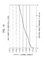
- the composition ratio it was understood that the Q factor, the withstand voltage, and the temperature coefficient of capacitance could be controlled in the range of from 173 to 183, 200 to 386 V, and -220 to -470 ppm/°C, respectively.
- the temperature coefficient of the capacitance can be controlled in the range of from -220 to -470 ppm/°C, and hence, this thin-film capacitor can be used as an element used for temperature compensation of an electronic device having a positive temperature coefficient, such as a varactor diode.
- the thin-film capacitor according to the present invention since at least one first dielectric thin-film and at least one second dielectric thin-film having a dielectric constant different from that of the first dielectric thin-film are disposed between a pair of electrodes, adjustment of the Q factor and the withstand voltage, and the temperature compensation can be performed by various combination of these two types of dielectric thin-films.
- the temperature coefficient of capacitance of the first dielectric thin-film when the absolute value of the temperature coefficient of capacitance of the first dielectric thin-film is 50 ppm/°C or less, the temperature coefficient of capacitance of the second dielectric thin-film is negative, and the absolute value thereof is 500 ppm/°C or more, adjustment of the temperature coefficient of the capacitor can be performed, and the capacitor can be used for temperature compensation applications.
- the second dielectric thin-film is composed of a polycrystalline material, and a plurality of crystalline grain boundaries formed of the crystalline grains in the polycrystalline material is not present in the thickness direction, a lower dielectric loss can be achieved in a high frequency band, and a Q factor in a high frequency band can be improved.
- the first dielectric thin-film can be formed so as to have a relative dielectric constant of 10 or less; a breakdown field strength of 5 MV/cm or more, and more preferably, 8 MV/cm or more; a Q of 200 or more, and more preferably, 1,000 or more at a frequency of 1 GHz or more; and a dielectric relaxation time of 1 second or more.
- the second dielectric thin-film can be formed so as to have a relative dielectric constant of 150 or less; and a Q of 50 or more, and more preferably, 100 or more at a frequency of 1 GHz or more.
- the first dielectric thin-film comprises SiO x N y
- the second dielectric thin-film comprises TiO x
- adjustment of the temperature coefficient of capacitance can be easily performed.
Landscapes
- Engineering & Computer Science (AREA)
- Power Engineering (AREA)
- Microelectronics & Electronic Packaging (AREA)
- Manufacturing & Machinery (AREA)
- Fixed Capacitors And Capacitor Manufacturing Machines (AREA)
- Inorganic Insulating Materials (AREA)
- Semiconductor Integrated Circuits (AREA)
- Investigating Or Analyzing Materials By The Use Of Electric Means (AREA)
- Ceramic Capacitors (AREA)
Abstract
Description

Claims (8)
- A temperature compensating thin-film capacitor comprising:wherein the first dielectric thin-film and the second dielectric thin-film are disposed between the pair of electrodes.at least one first dielectric thin-film;at least one second dielectric thin-film having a relative dielectric constant different from that of the first dielectric thin-film; anda pair of electrodes;
- A temperature compensating thin-film capacitor according to Claim 1, wherein the absolute value of the temperature coefficient of capacitance of the first dielectric thin-film is 50 ppm/°C or less, and the temperature coefficient of capacitance of the second dielectric thin-film is negative and has an absolute value of 500 ppm/°C or more.
- A temperature compensating thin-film capacitor according to Claim 1 or 2, wherein the second dielectric thin-film comprises a polycrystalline material having a number of crystalline grains which form a number of crystalline grain boundaries, and the number of the crystalline grain boundaries is less than ten in the thickness direction of the second dielectric thin-film.
- A temperature compensating thin-film capacitor according to Claim 1, 2 or 3, wherein the first dielectric thin-film has a relative dielectric constant of 10 or less, a breakdown field strength of 5 MV/cm or more, a Q factor of 200 or more at a frequency of 1 GHz or more, and a dielectric relaxation time of 1 second or more.
- A temperature compensating thin-film capacitor according to any preceding claim, wherein the second dielectric thin-film has a relative dielectric constant of 150 or less, and a Q factor of 50 or more at a frequency of 1 GHz or more.
- A temperature compensating thin-film capacitor according to any preceding claim, wherein the second dielectric thin-comprises SiOxNy.
- A temperature compensating thin-film capacitor according to any preceding claim, wherein the second dielectric thin-film comprises one of TiOx and CaTiO3.
- A temperature compensating thin-film capacitor according to any preceding claim, wherein, as the first and the second thin-films disposed between the pair of electrodes, the first dielectric thin-films are each provided on each electrode, and the second dielectric thin-film is provided between the first dielectric thin-films.
Applications Claiming Priority (2)
| Application Number | Priority Date | Filing Date | Title |
|---|---|---|---|
| JP2000256405 | 2000-08-25 | ||
| JP2000256405A JP2002075783A (en) | 2000-08-25 | 2000-08-25 | Thin film capacitor for temperature compensation |
Publications (2)
| Publication Number | Publication Date |
|---|---|
| EP1182696A2 true EP1182696A2 (en) | 2002-02-27 |
| EP1182696A3 EP1182696A3 (en) | 2005-05-25 |
Family
ID=18745021
Family Applications (1)
| Application Number | Title | Priority Date | Filing Date |
|---|---|---|---|
| EP01306733A Withdrawn EP1182696A3 (en) | 2000-08-25 | 2001-08-07 | Temperature compensating thinfilm capacitor |
Country Status (5)
| Country | Link |
|---|---|
| US (1) | US6477036B2 (en) |
| EP (1) | EP1182696A3 (en) |
| JP (1) | JP2002075783A (en) |
| KR (1) | KR100450101B1 (en) |
| CN (1) | CN1197103C (en) |
Families Citing this family (24)
| Publication number | Priority date | Publication date | Assignee | Title |
|---|---|---|---|---|
| JP2004095638A (en) * | 2002-08-29 | 2004-03-25 | Fujitsu Ltd | Thin film decoupling capacitor and method of manufacturing the same |
| US20040061990A1 (en) * | 2002-09-26 | 2004-04-01 | Dougherty T. Kirk | Temperature-compensated ferroelectric capacitor device, and its fabrication |
| US20060000542A1 (en) * | 2004-06-30 | 2006-01-05 | Yongki Min | Metal oxide ceramic thin film on base metal electrode |
| US7216406B2 (en) * | 2004-09-29 | 2007-05-15 | Intel Corporation | Method forming split thin film capacitors with multiple voltages |
| US7290315B2 (en) * | 2004-10-21 | 2007-11-06 | Intel Corporation | Method for making a passive device structure |
| US20060099803A1 (en) * | 2004-10-26 | 2006-05-11 | Yongki Min | Thin film capacitor |
| US9572258B2 (en) * | 2004-12-30 | 2017-02-14 | Intel Corporation | Method of forming a substrate core with embedded capacitor and structures formed thereby |
| US20060220177A1 (en) * | 2005-03-31 | 2006-10-05 | Palanduz Cengiz A | Reduced porosity high-k thin film mixed grains for thin film capacitor applications |
| US7629269B2 (en) * | 2005-03-31 | 2009-12-08 | Intel Corporation | High-k thin film grain size control |
| US7288459B2 (en) * | 2005-03-31 | 2007-10-30 | Intel Corporation | Organic substrates with integral thin-film capacitors, methods of making same, and systems containing same |
| US7372126B2 (en) * | 2005-03-31 | 2008-05-13 | Intel Corporation | Organic substrates with embedded thin-film capacitors, methods of making same, and systems containing same |
| US7375412B1 (en) | 2005-03-31 | 2008-05-20 | Intel Corporation | iTFC with optimized C(T) |
| US7453144B2 (en) * | 2005-06-29 | 2008-11-18 | Intel Corporation | Thin film capacitors and methods of making the same |
| JP2010192466A (en) * | 2007-04-27 | 2010-09-02 | Nec Corp | Wide band capacitance element |
| KR101420773B1 (en) * | 2009-07-15 | 2014-07-17 | 주성엔지니어링(주) | Electro-optic device and method for manufacturing the same |
| JP5120406B2 (en) * | 2010-03-31 | 2013-01-16 | Tdk株式会社 | Ceramic electronic component and method for manufacturing ceramic electronic component |
| US10056609B2 (en) | 2011-07-11 | 2018-08-21 | Quantumscape Corporation | Solid state energy storage devices |
| US9087645B2 (en) * | 2012-01-30 | 2015-07-21 | QuantrumScape Corporation | Solid state energy storage devices |
| JP5441020B1 (en) * | 2012-08-29 | 2014-03-12 | Toto株式会社 | Electrostatic chuck |
| JP5936087B2 (en) * | 2014-10-07 | 2016-06-15 | 国立大学法人 岡山大学 | Thin film hydrogen gas sensor |
| US10115527B2 (en) * | 2015-03-09 | 2018-10-30 | Blackberry Limited | Thin film dielectric stack |
| US10122357B2 (en) | 2016-11-14 | 2018-11-06 | Ford Global Technologies, Llc | Sensorless temperature compensation for power switching devices |
| US11942418B2 (en) * | 2021-07-23 | 2024-03-26 | Taiwan Semiconductor Manufacturing Company, Ltd. | Semiconductor structure and method for making the same |
| JP7682759B2 (en) * | 2021-09-30 | 2025-05-26 | Tdk株式会社 | Thin film capacitor, power supply module and electronic device |
Family Cites Families (15)
| Publication number | Priority date | Publication date | Assignee | Title |
|---|---|---|---|---|
| US88216A (en) * | 1869-03-23 | Improved crushing and q-rindino-machine | ||
| JPS4870855A (en) * | 1971-12-29 | 1973-09-26 | ||
| JPS5873908A (en) | 1981-10-28 | 1983-05-04 | ティーディーケイ株式会社 | High frequency dielectric porcelain composition |
| US4423087A (en) * | 1981-12-28 | 1983-12-27 | International Business Machines Corporation | Thin film capacitor with a dual bottom electrode structure |
| JPS62222512A (en) * | 1986-03-20 | 1987-09-30 | キヤノン株式会社 | dielectric material |
| JPS63110618A (en) * | 1986-10-28 | 1988-05-16 | 沖電気工業株式会社 | Laminated microwave dielectric porcelain compound |
| EP0356212B1 (en) | 1988-08-25 | 1993-04-28 | Matsushita Electric Industrial Co., Ltd. | Thin-film capacitor and method of manufacturing a hybrid microwave integrated circuit |
| JPH03252160A (en) * | 1990-02-28 | 1991-11-11 | Nec Corp | Capacitor, capacitor network, and r-c network |
| US6088216A (en) * | 1995-04-28 | 2000-07-11 | International Business Machines Corporation | Lead silicate based capacitor structures |
| US5638252A (en) * | 1995-06-14 | 1997-06-10 | Hughes Aircraft Company | Electrical device and method utilizing a positive-temperature-coefficient ferroelectric capacitor |
| DE69624042T2 (en) | 1995-06-16 | 2003-06-05 | At&T Ipm Corp., Coral Gables | TiO2-doped, Ta2O5-containing dielectric material and components containing it |
| US5978207A (en) * | 1996-10-30 | 1999-11-02 | The Research Foundation Of The State University Of New York | Thin film capacitor |
| JP3123448B2 (en) * | 1996-11-13 | 2001-01-09 | 日本電気株式会社 | Thin film capacitors |
| US6236102B1 (en) * | 1997-12-13 | 2001-05-22 | Samsung Electro-Mechanics Co., Ltd. | Chip type thin film capacitor, and manufacturing method therefor |
| JP2000183289A (en) * | 1998-12-18 | 2000-06-30 | Murata Mfg Co Ltd | Control of characteristics for dielectric element |
-
2000
- 2000-08-25 JP JP2000256405A patent/JP2002075783A/en not_active Withdrawn
-
2001
- 2001-08-07 EP EP01306733A patent/EP1182696A3/en not_active Withdrawn
- 2001-08-09 CN CNB011239670A patent/CN1197103C/en not_active Expired - Fee Related
- 2001-08-13 KR KR10-2001-0048689A patent/KR100450101B1/en not_active Expired - Fee Related
- 2001-08-16 US US09/930,862 patent/US6477036B2/en not_active Expired - Fee Related
Also Published As
| Publication number | Publication date |
|---|---|
| CN1197103C (en) | 2005-04-13 |
| KR100450101B1 (en) | 2004-09-24 |
| JP2002075783A (en) | 2002-03-15 |
| KR20020016508A (en) | 2002-03-04 |
| US20020080551A1 (en) | 2002-06-27 |
| US6477036B2 (en) | 2002-11-05 |
| EP1182696A3 (en) | 2005-05-25 |
| CN1340832A (en) | 2002-03-20 |
Similar Documents
| Publication | Publication Date | Title |
|---|---|---|
| US6477036B2 (en) | Temperature compensating thin-film capacitor | |
| Sengupta et al. | Breakthrough advances in low loss, tunable dielectric materials | |
| US6605515B2 (en) | Method for manufacturing thin-film capacitor for performing temperature compensation of junction capacitance of semiconductor device | |
| US5767564A (en) | Semiconductor device with a decoupling capacitor mounted thereon having a thermal expansion coefficient matched to the device | |
| EP0794542B1 (en) | Dielectric ceramic and monolithic ceramic electronic part using the same | |
| EP1997115B8 (en) | Ceramic component element and method for manufacturing the same | |
| JP7060213B2 (en) | Dielectric porcelain composition and multilayer ceramic capacitors containing it | |
| US6556421B2 (en) | Temperature-compensating thin-film capacitor and electronic device | |
| US6008981A (en) | Monolithic ceramic capacitor | |
| US7277003B2 (en) | Electrostatic discharge protection component | |
| US12597567B2 (en) | Single layer capacitor | |
| US20230246040A1 (en) | Variable electronic element and circuit device | |
| WO2004044934A1 (en) | Thin film capacitor for reducing power supply noise | |
| JPS6253923B2 (en) | ||
| TW564439B (en) | Electro-ceramic component | |
| JP3512609B2 (en) | Thin film capacitors and capacitors | |
| JPS6094716A (en) | Thin film condenser | |
| CN110382441A (en) | Dielectric composition and electronic device | |
| JPH06120007A (en) | Laminated type varistor | |
| Szedon et al. | Dielectric films for capacitor applications in electronic technology | |
| HK40123961A (en) | Single layer capacitor | |
| JP2936925B2 (en) | Method for producing multilayer semiconductor ceramic composition | |
| CN114678218A (en) | Multilayer electronic assemblies and dielectric compositions | |
| Yamamichi et al. | An Ultra-Thin Decoupling Capacitor with SrTiO 3 thin film on polyimide | |
| WO2004044935A1 (en) | Capacitor composite circuit element and ic card multilayer capacitor |
Legal Events
| Date | Code | Title | Description |
|---|---|---|---|
| PUAI | Public reference made under article 153(3) epc to a published international application that has entered the european phase |
Free format text: ORIGINAL CODE: 0009012 |
|
| AK | Designated contracting states |
Kind code of ref document: A2 Designated state(s): AT BE CH CY DE DK ES FI FR GB GR IE IT LI LU MC NL PT SE TR |
|
| AX | Request for extension of the european patent |
Free format text: AL;LT;LV;MK;RO;SI |
|
| PUAL | Search report despatched |
Free format text: ORIGINAL CODE: 0009013 |
|
| RIC1 | Information provided on ipc code assigned before grant |
Ipc: 7H 01L 21/02 B Ipc: 7H 01G 4/00 B Ipc: 7H 01G 4/20 B Ipc: 7H 01G 4/258 A |
|
| AK | Designated contracting states |
Kind code of ref document: A3 Designated state(s): AT BE CH CY DE DK ES FI FR GB GR IE IT LI LU MC NL PT SE TR |
|
| AX | Request for extension of the european patent |
Extension state: AL LT LV MK RO SI |
|
| 17P | Request for examination filed |
Effective date: 20050629 |
|
| AKX | Designation fees paid |
Designated state(s): DE FI FR GB SE |
|
| STAA | Information on the status of an ep patent application or granted ep patent |
Free format text: STATUS: THE APPLICATION IS DEEMED TO BE WITHDRAWN |
|
| 18D | Application deemed to be withdrawn |
Effective date: 20060808 |