The invention relates to a method of generating a clock signal (clk) from an optical input signal
(1) that is divided up optically into two channels, one for data extraction to generate an electrical
data signal (11) and one for clock extraction to generate an electrical first clock signal (21) and
also a digital optical receiver having an optical channel for data extraction and an optical channel
for clock extraction, both channels each comprising means for converting the optical received
signal into an electrical signal.
During the transmission of optical digital signals, various dispersion effects occur that are caused
by the optical waveguides of the optical transmission system. In addition, the useful power
decreases with increasing transmission distance with respect to the noise power because of the
attenuation properties of the optical waveguide. At high bit rate (gigabit range), in particular,
these effects result in falsification of the transmitted data signals. Optical receivers that are used
in such a transmission system are confronted with the task of evaluating even falsified signals
and, in this connection, to permit only low bit error rates. For this purpose, the received optical
signal is converted into an electrical signal, sampled with the signal clock and then conveyed to a
decision circuit in which a digital decision is made by a comparison with a threshold. A
substantial problem in this connection is the recovery of the signal clock from the transmitted
signal. Existing receivers frequently solve the problem in that the received optical signal is first
converted into an electrical signal by means of a photodiode and is fed to the said decision
circuit. The said electrical signal is cut off by means of a so-called splitter and fed to a clock
recovery circuit. The clock or sampling signal extracted by the clock recovery circuit is fed to the
said decision device, where the data signal is then sampled. It has been found, however, that, in
particular at bit rates above 5 gigabit, phase and amplitude interferences in the electrical data
signals occur because of increasing electromagnetic radiation from the highly integrated circuits
of the receiver. These errors result in an increased bit error rate.
EP 0 817 408 A1 discloses a receiver for an optical digital transmission system in which the
abovementioned interferences are reduced, inter alia, as a result of the fact that the received
optical signal is divided up by means of an optical splitter into two optical signals for a channel
for data extraction and a channel for other functions, in particular clock recovery, respectively.
The conversion into electrical signals by means of a photodiode then takes place separately in
each channel. A far lower mutual electromagnetic interference of the said channels is thereby
achieved. A remaining problem is, however, presented by different signal delay times in the two
channels that are due, for example, to temperature differences or to ageing, in particular, of the
photodiodes. As a result, a phase shift of the clock signal occurs with respect to the data signal.
This then results in incorrect digital identifications in the decision circuit and consequently also
in a higher bit error rate.
The object of the invention is to modify an optical receiver of the type mentioned in the last
section so that an adaptive phase correction of the clock signal is achieved with which the data
signal can then be correctly sampled.
According to the invention, this object is achieved by a method of generating a clock signal from
an optical input signal according to the teaching of Claim 1 and also a receiver according to the
teaching of Claim 3.
Further advantageous embodiments of the invention are to be found in the dependent claims and
the description.
The invention is explained further below by reference to the drawings, in which:
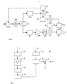
- Figure 1
- shows a block circuit diagram of an optical receiver according to the invention
and
- Figure 2
- shows a block circuit diagram of a basic circuit for determining the phase
difference.
Figure 1 shows an optical input signal 1 that first passes through a controllable optical amplifier
AGC and a band-pass filter BPF before it is passed as an amplified and filtered signal 1' to the
input of an optical coupler OC. The optical splitter has two outputs, each of the outputs being
connected to one input in each case of a photodiode PID1 and PID2. The output of the
photodiode PD 1 is connected via an (electrical) amplifier AMP and a low-pass filter LPF to the
input of an (electrical) splitter SP1 having two outputs, one output being connected to an input of
a decision circuit DC. At the output of the decision circuit there is an output signal 2 of the
optical receiver. The second output of the splitter SP1 carries a data signal 11 that is fed to one of
the two input signals of a phase difference circuit PD. The output of the photodiode PID2 is
connected to the input of an (electrical) splitter SP3 having two outputs, the one output being
connected via a gain controller LC to the control input of the optical amplifier AGC and the
other output being connected to the input of a clock recovery circuit CR. The output of the clock
recovery circuit CR is connected to the input of a further (electrical) splitter SP2 having two
outputs. One of these outputs is connected to one of two inputs of a phase correction circuit
PHC, whose output carrying the clock signal clk is in turn connected to the second input of the
decision circuit DC. The second output of the splitter SP2 carrying the first clock signal 21 is
connected to the second input of the phase difference circuit PD. The output of the phase
difference circuit PD carrying the delay signal ds is connected to the second input of the phase
correction circuit PHC.
The optical splitting of the amplified and filtered signal 1' over a data extraction channel and a
clock recovery channel, respectively, is disclosed in the abovementioned EP 0 817 408 A1. The
optical input signal 1 is a binary signal comprising a sequence of code elements that assume only
the values "0" or "1". This sequence is transmitted at the rate r = 1/T, T being the time duration,
referred to below also as clock time, for the transmission of a code element. The rate r is also
referred to as symbol frequency. A light pulse is transmitted for each code element having the
value "1". In this connection, the light pulses can have various shapes. Frequently, the pulse has
an approximately rectangular shape, with a power that is continuous during the entire time
duration T. Since such a signal does not return to zero for the successive transmission of "1", it is
also referred to as NRZ (no return to zero) signal. A further, frequent pulse shape is the so-called
soliton pulse whose duration is markedly shorter than the clock time T. The pulse shape is
unimportant for the invention; for example, NR signals, so-called RZ signals (return to zero) and
soliton signals can be processed.
Compared to the prior art, the receiver disclosed differs in that the first clock signal 21 is fed not
directly to the decision circuit DC, but via the phase correction circuit PHC. For this purpose, the
data signal 11 is tapped off via the splitter SP1 as close as possible to the input of the decision
circuit and the first clock signal 21 is tapped off via the splitter SP2 as close as possible to the
input of the phase correction circuit PHC, the phase difference of the two signals is determined
in the phase difference circuit PD and a corresponding delay signal ds is fed to the phase
correction circuit PHC. The phase correction circuit PHC delays the clock signal clk to such an
extent that it is in phase with the data signal to be sampled at the input of the decision circuit.
Figure 2 shows an exemplary block circuit diagram of the phase difference circuit PD from
Figure 1. The data signal 11 is fed via a first attenuation element 31, a narrow-band amplifier 32,
a frequency doubler 33 and a band-pass filter 34 to one of the two inputs of a phase comparator
42. The first clock signal 21 is fed via a second attenuation element 41 to the second input of the
phase comparator 42, whose output is fed to an adder 43. In the adder 43, an adjustable offset
value 12 is added and the sum of the two signals is outputted as delay signal ds.
The attenuation elements 31 and 41 reduce the signal power of the signals 11 and 21,
respectively. This reduction in the signal power serves to match the signal power to the phase
comparator 42. The frequency spectrum of the data signal 11 does not contain any spectral lines
or (approximately) discrete spectrum components at the points f = 1/T and f = -1/T (clock
frequency = 1/T), but it does at the points of the respective half frequencies f = 1/2T and
f= -1/2T. No direct recovery of the clock signal from the data signal 11 is therefore possible as a
result of simple filtering. For this purpose, the signal 11, after attenuation of the first attenuation
element 31, is first fed to the narrow-band amplifier 32, which performs a symmetrical narrow-band
amplification around the frequency values f = 1/2T and f = -1/2T. As a result of the
subsequent frequency doubling in the frequency doubler 33, a signal is produced that has spectral
lines at the points 1/T and -1/T. The frequency can be doubled, for example, by multiplying the
signal. Narrow-band filtering around the frequencies 1/T and -1/T now produces a sinusoidal
signal having the angular frequency 2*pi/T. The other frequency components, which are not
filtered out, result in an undesirable jitter of the angular frequency. The band-pass filter 34 is of
as narrow-band and steep-edged design as possible in order substantially to avoid said jitter. The
signal obtained is now compared in the phase comparator 42 with the likewise cosinusoidal first
clock signal 21. Depending on the phase difference found, the phase comparator 42 emits a first
delay signal. To align the entire circuit according to Figure 1, an adjustable offset value 12 is
added to this signal and the sum is fed as delay signal ds to the phase correction circuit PHC
shown in Figure 1. If the phase of the data signal 21 leads the phase of the clock signal 11, i.e. a
negative delay value is found, the clock signal is delayed by the time T minus the absolute value
of the delay value ds found.
In an alternative embodiment, to avoid the necessary case decision between positive and negative
"delays", insertion of a fixed delay element in the data extraction channel ensures that only
positive delays in the clock signal have to be undertaken.
In a further alternative embodiment, the data signal 11 is first differentiated after traversing the
attenuation element 31 and then rectified by means of a rectifier or squaring circuit. The signal
thereby obtained now has discrete spectral components around the frequencies 1/T and -1/T and
is fed to the band-pass filter 34. This circuit is suitable, in particular, if the data signal 11 has a
substantially ideal NRZ pulse shape, for which the circuit described in the last section is less
suitable because of the absence of discrete frequency components.