EP1179888A1 - Pll circuit - Google Patents
Pll circuit Download PDFInfo
- Publication number
- EP1179888A1 EP1179888A1 EP01118698A EP01118698A EP1179888A1 EP 1179888 A1 EP1179888 A1 EP 1179888A1 EP 01118698 A EP01118698 A EP 01118698A EP 01118698 A EP01118698 A EP 01118698A EP 1179888 A1 EP1179888 A1 EP 1179888A1
- Authority
- EP
- European Patent Office
- Prior art keywords
- output
- input
- frequency
- pll
- transistor
- Prior art date
- Legal status (The legal status is an assumption and is not a legal conclusion. Google has not performed a legal analysis and makes no representation as to the accuracy of the status listed.)
- Withdrawn
Links
- 230000004044 response Effects 0.000 claims description 6
- 238000010276 construction Methods 0.000 abstract description 18
- 238000001514 detection method Methods 0.000 abstract description 3
- 239000003990 capacitor Substances 0.000 description 14
- 238000010586 diagram Methods 0.000 description 8
- 230000010355 oscillation Effects 0.000 description 5
- 238000009825 accumulation Methods 0.000 description 2
- 238000012986 modification Methods 0.000 description 2
- 230000004048 modification Effects 0.000 description 2
- 238000004904 shortening Methods 0.000 description 2
- 230000008859 change Effects 0.000 description 1
- 238000006243 chemical reaction Methods 0.000 description 1
- 230000003247 decreasing effect Effects 0.000 description 1
- 230000006866 deterioration Effects 0.000 description 1
- 230000005283 ground state Effects 0.000 description 1
- 238000000034 method Methods 0.000 description 1
- 230000008569 process Effects 0.000 description 1
- 230000001629 suppression Effects 0.000 description 1
- 230000001360 synchronised effect Effects 0.000 description 1
Images



Classifications
-
- H—ELECTRICITY
- H03—ELECTRONIC CIRCUITRY
- H03L—AUTOMATIC CONTROL, STARTING, SYNCHRONISATION OR STABILISATION OF GENERATORS OF ELECTRONIC OSCILLATIONS OR PULSES
- H03L7/00—Automatic control of frequency or phase; Synchronisation
- H03L7/06—Automatic control of frequency or phase; Synchronisation using a reference signal applied to a frequency- or phase-locked loop
- H03L7/08—Details of the phase-locked loop
- H03L7/085—Details of the phase-locked loop concerning mainly the frequency- or phase-detection arrangement including the filtering or amplification of its output signal
- H03L7/095—Details of the phase-locked loop concerning mainly the frequency- or phase-detection arrangement including the filtering or amplification of its output signal using a lock detector
-
- H—ELECTRICITY
- H03—ELECTRONIC CIRCUITRY
- H03L—AUTOMATIC CONTROL, STARTING, SYNCHRONISATION OR STABILISATION OF GENERATORS OF ELECTRONIC OSCILLATIONS OR PULSES
- H03L7/00—Automatic control of frequency or phase; Synchronisation
- H03L7/06—Automatic control of frequency or phase; Synchronisation using a reference signal applied to a frequency- or phase-locked loop
- H03L7/08—Details of the phase-locked loop
- H03L7/10—Details of the phase-locked loop for assuring initial synchronisation or for broadening the capture range
- H03L7/107—Details of the phase-locked loop for assuring initial synchronisation or for broadening the capture range using a variable transfer function for the loop, e.g. low pass filter having a variable bandwidth
- H03L7/1075—Details of the phase-locked loop for assuring initial synchronisation or for broadening the capture range using a variable transfer function for the loop, e.g. low pass filter having a variable bandwidth by changing characteristics of the loop filter, e.g. changing the gain, changing the bandwidth
-
- H—ELECTRICITY
- H03—ELECTRONIC CIRCUITRY
- H03L—AUTOMATIC CONTROL, STARTING, SYNCHRONISATION OR STABILISATION OF GENERATORS OF ELECTRONIC OSCILLATIONS OR PULSES
- H03L2207/00—Indexing scheme relating to automatic control of frequency or phase and to synchronisation
- H03L2207/12—Indirect frequency synthesis using a mixer in the phase-locked loop
-
- Y—GENERAL TAGGING OF NEW TECHNOLOGICAL DEVELOPMENTS; GENERAL TAGGING OF CROSS-SECTIONAL TECHNOLOGIES SPANNING OVER SEVERAL SECTIONS OF THE IPC; TECHNICAL SUBJECTS COVERED BY FORMER USPC CROSS-REFERENCE ART COLLECTIONS [XRACs] AND DIGESTS
- Y10—TECHNICAL SUBJECTS COVERED BY FORMER USPC
- Y10S—TECHNICAL SUBJECTS COVERED BY FORMER USPC CROSS-REFERENCE ART COLLECTIONS [XRACs] AND DIGESTS
- Y10S331/00—Oscillators
- Y10S331/02—Phase locked loop having lock indicating or detecting means
Definitions
- the invention relates to a PLL (phase-lock loop) circuit, and more particularly to a PLL circuit which can shorten lock-up time.
- PLL phase-lock loop
- Shortening the lock-up time (or settling time) of a phase comparator circuit is required of PLL circuits used in ICs (or LSIs) of mobile radio equipment and the like.
- Shortened look-up time time elapsed until the frequency difference becomes zero (0)
- c/N signal-to-noise ratio
- VCO voltage controlled oscillator
- Fig. 1 shows a conventional PLL circuit.
- An adder 102 is connected to a current output-type phase comparator (PD) 101 into which an input signal frequency fIF is input.
- a constant-current source 103, a reset switch 104, and a low pass filter (LPF) 105 are connected to the adder 102.
- VCO 106 for outputting a VCO output frequency fRF is connected to LPF 105.
- a coupler 107 is connected to this VCO 106, and a mixer 108, into which a local signal frequency fLO is input, is connected between the coupler 107 and PD 101.
- PD 101, LPF 105, VCO 106, and the mixer 108 basically constitute the PLL circuit.
- This construction is characterized by providing the constant current source 103 and the reset switch 104.
- the constant current source 103 functions to apply constant current to LPF 105.
- the phase of the input signal frequency fIF is compared with the phase of the reference signal frequency fRF, and a current proportional to the phase difference is output.
- a reset switch 104 is turned ON.
- charges accumulated in a capacitor of LPF 105 are discharged, and VCO control voltage is brought to the ground state (0 V).
- the reset switch 104 is turned OFF, and charges are accumulated in the capacitor within LPF 105 by a constant-current source 103 to increase the accumulation speed (to shorten the time elapsed until the VCO control voltage is increased from 0 V to a desired voltage). This can shorten the lock-up time.
- a constant current output from the constant current source 103 is added to the output current of PD 101, and the total current is input into LPF 105.
- LPF 105 unnecessary harmonic components and noises in the input total current are removed, followed by conversion to DC voltage which is input into VCO 106.
- the output frequency fRF of VCO 106 is input into the mixer 108 through the coupler 107.
- a mixer 108 mixes an output frequency fRF with a local signal frequency fLO.
- a direct current component of the output current from PD 101 accumulates charges in the capacitor of LPF 105, and the output voltage is input into VCO 105.
- the constant current output from the constant current source 103 is also accumulated in the above capacitor.
- the accumulation speed of charges in the capacitor is increased. Therefore, the settling time of PLL is shortened.
- Japanese Patent Laid-Open Nos. 288518/1988 and 259902/1993 propose a PLL circuit having a construction such that the time constant of LPF is variable and, at the time of the turn-on of power and at the time of out-of-locking upon a change of the division ratio of a frequency divider, the time constant is changed and, after locking, the time constant is returned to the previous value.
- the constant current source 103 is operated.
- the set current of the constant current source 103 is excessive, an increase in output voltage of the phase comparator 101 is faster than the following of PLL per se and PLL is unlocked. Therefore, a limitation is imposed on current setting.
- phase comparator 101 cannot sometimes maintain a phase difference of 90 degrees relative to two signals of input fIF and fREF. This poses a problem of an increase in noise and harmonic spurious on the output side.
- a PLL circuit comprises:
- the switch means switches the loop filter so that the response is enhanced, whereby the input voltage of VCO is rapidly increased.
- the PLL circuit is lockable, the loop filter is brought to a usual operation state.
- a PLL circuit comprises:
- the switch means turns on the constant current source to allow a current to flow from the constant current source to the loop filter, thereby permitting the capacitor of the loop filter to be rapidly charged.
- the constant current source is turned off and is separated from the input terminal of the loop filter.
- Fig. 2 shows a first preferred embodiment of the PLL circuit according to the invention.
- the PLL circuit according to the invention is of an analog system and comprises: a phase comparator 1 into which a reference signal f REF (first input signal) and a mixer output signal f MIX OUT (second input signal) are input; a mixer 2 for generating a mixer output signal f MIX OUT based on a local signal frequency f L0 ; a band pass filter (BPF) 3 connected to the phase comparator 1; an offset differential pair circuit 4 connected to this BPF 3; a changeover switch 5 (switch means) wherein switching is carried out by the offset differential pair circuit 4; a loop filter (LPF) 6 connected to the phase comparator 1; and VCO 7 which generates a VCO output signal f OUT based on the output voltage of this LPF 6 and, in addition, applies the VCO output signal f OUT to the mixer 2.
- a phase comparator 1 into which a reference signal f REF (first input signal) and a mixer output signal f MIX OUT (second input signal) are input
- the phase comparator 1 is provided with a circuit having a gilbert cell mixer construction, and an input terminal of BPF 3 is connected to an output terminal of the circuit.
- BPF 3 and the offset differential pair circuit 4 constitute one detector.
- LPF 6 is constituted using a ruggrite filter or an active filter. When the changeover switch 5 is ON, LPF 6 is set to a time constant during the usual operation, while when the changeover switch 5 is OFF, LPF 6 is separated from the ground and is set to a time constant value smaller than the above time constant.
- Fig. 3 shows frequency characteristics of BPF 3.
- a first cut-off frequency fc1 is set so as to conform to the frequency range in the capture range of the PLL circuit
- a second cut-off frequency fc2 is set so as to conform to the operation frequency range (synchronous holding range) of VCO 7.
- the PLL circuit is judged to be lockable.
- the VCO output signal f OUT output from VCO 7 is input into the mixer 2 in a feedback loop.
- a mixer output signal f NIX OUT
- the phase comparator 1 generates a voltage signal corresponding to the phase difference caused between the reference signal f REF and the mixer output signal f MIX OUT and inputs the voltage signal into LPF 6.
- LPF 6 has a predetermined time constant, and, in addition, functions to remove an unnecessary signal component contained in the input signal and to generate direct current output voltage. This direct current output voltage is applied as control voltage to VCO 7.
- PLL becomes a lock state.
- Another output signal of the phase comparator 1 is input into BPF 3, and only a signal having a predetermined frequency region is input into the offset differential pair circuit 4.
- the offset differential pair circuit 4 generates a signal for switching the changeover switch 5, and sends a control signal to the changeover switch 5.
- LPF 6 is set to a small time constant value and is operated so that the response is enhanced. This can accelerate the lead-in process until the VCO voltage in VCO 7 reaches a desired value.
- VCO 7 has been led to desired VCO voltage, the PLL circuit is locked in.
- LPF 6 which can switch the time constant, the lock-up time is shortened, and, in addition, noise or harmonic spurious is not increased. Further, since there is no need to perform external control, this is also suitable for IC construction.
- the response of LPF 6 may be enhanced by increasing the output voltage of LPF 6 in a short time to a large value.
- the value of a capacitor or resistor constituting the time constant circuit of LPF 6 is varied. That is, the time constant is increased in the case of a value falling within the capture range of the PLL circuit, while the time constant is decreased in the case of a value outside the capture range.
- the charge time of the capacitor is made shorter than the usual charge time.
- a construction may be adopted wherein two capacitors may be connected parallel to each other and one of the two capacitors is turned ON/OFF.
- a construction may be adopted wherein two resistors are connected in series and one of the two resistors is shortcircuited or insertion-connected.
- Fig. 4 shows the details of an offset differential pair circuit 4.
- the offset differential pair circuit 4 comprises a first differential amplifier 4a and a second differential amplifier 4b.
- the first differential amplifier 4a comprises transistors Q1, Q2 and a resistor Rc1
- the second differential amplifier 4b comprises transistors Q3, Q4 and a resistor Rc2.
- the transistors Q2, Q4 have an emitter area obtained by multiplying the emitter area of the transistors Q1, Q3 by N. The use of transistors having this structure can provide characteristics shown in Fig. 5.
- each base of the other transistors is grounded, or alternatively, a predetermined bias voltage is applied thereto.
- Each emitter of the transistors Q1 to Q4 is grounded.
- the collector of the transistor Q1 is connected to the collector of the transistor Q3, and, likewise, the collector of the transistor Q2 is connected to the collector of the transistor Q4.
- the collector of the transistor Q1 and the collector of the transistor Q3 are connected to each other, and are connected to a power source V s through a resistor Rc1.
- the collector of the transistor Q2 and the collector of the transistor Q4 are connected to each other, and are connected to a power source through a resistor Rc2.
- Fig. 5 shows characteristics of input voltage vs output voltage of the offset differential pair circuit 4 shown in Fig. 4.
- the output difference voltage V out is brought to zero (0).
- the input voltage V in is not more than about 200 mV
- is output as an output signal f pd out of the phase comparator 1.
- This output signal is subjected to the following treatment according to whether or not the output signal falls within the capture range of the PLL circuit.
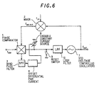
- Fig. 6 shows the second preferred embodiment of the invention. Like parts are identified with the same reference numerals throughout Fig. 6 and Fig. 2, and the overlapped explanation will be omitted.
- This preferred embodiment is characterized in that LPF 6 is replaced by LPF 10, which does not undergo any external control, that is, has a fixed time constant, a variable constant current source 8 is connected between the output line of the phase comparator 1 and the power source VS, and, in addition, a reset switch 9 was disposed instead of the changeover switch 5. Since the variable constant current source 8 is used, current output type is used in the phase comparator 1. The variable constant current source 8 is controlled by the offset differential pair circuit 4. There is no particular limitation on current setting of the variable constant current source 8. Preferably, however, the current is set to a value suitable for the circuit used.
- the reset switch 9 When the PLL circuit is not in operation (for example, at the time of the switching of the frequency channel and at the time of turn-on of the power), the reset switch 9 is automatically turned ON by a detector and a controller (not shown). and the charges accumulated in the capacitor in LPF 10 are discharged to ground. This brings the control voltage of VCO 7 to zero (0) V.
- the use of the reset switch 9 is indispensable. The provision of the reset switch 9 can eliminate the limitation of the current value of the variable constant current source 8, and the follow-up with respect to a variation in frequency, in such a direction that causes a lowering in voltage of VCO, can be enhanced.
- the variable constant current source 8 supplies current to LPF 10, and charges the capacitor within LPF 10 independently of the output of the phase comparator 1. This permits the output voltage of LPF 10 to be linearly increased from 0 V with the elapse of time. Upon this operation, the output signal f OUT of VCO 7 is increased from the lower limit of the operation oscillation frequency. In the course of an increase in oscillation frequency, when the output signal f pd out of the phase comparator 1 falls within the capture range of the PLL circuit, output takes place in BPF 3 and the offset differential pair circuit 4, the operation of the variable constant current source 8 is turned OFF, and the PLL circuit is led to lock-in.
- the control voltage (input voltage) of VCO 7 is brought to zero (0) V, while, at the time of the operation of PLL, the control voltage of VCO 7 is rapidly increased from 0 V to a value around a desired voltage by the current supplied from the variable constant current source 8.
- the operation of the variable constant current source 8 is turned OFF and the PLL circuit is led to lock-in by the original PLL operation. This shortens the lock-up time. Further, even when lock-up has been done using the constant current source, there is no limitation on current setting. Furthermore, noise and harmonic spurious are reduced.
- Fig. 7 shows a third preferred embodiment of the invention.
- the reset switch 9 When PLL is not in the state of operation (for example, at the time of switching of the frequency channel and at the time of the turn-on of the power), the reset switch 9 is turned ON, the sixth loop filter are charged, and the control voltage of VCO 7 is increased to the level of the power voltage.
- the reset switch 9 When the PLL circuit is operated, the reset switch 9 is turned OFF. Just as the reset switch 9 has been turned OFF, the control voltage of VCO 7 is 0 V and the output signal f out of VCO 7 is in the upper limit of the operation oscillation frequency.
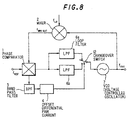
- the time constant of LPF 6 is switched by the changeover switch 5. This can be changed to a construction shown in Fig. 8.
- Fig. 8 shows a variant of the first preferred embodiment.
- This preferred embodiment is characterized in that two LPFs 6a, 6b are used as LPF and are switched by a changeover switch 12.
- LPF 6a the circuit time constant is small, and the band width is large, while, in LPF 6b, the circuit time constant is large and the band width is narrow.
- LPF 6a is selected by the changeover switch 12.
- LPF 6b is selected.
- the circuit time constant can be freely set for each of LPFs, and, thus, the degree of freedom in design can be advantageously improved.
- a detector detects such a state that the PLL circuit is not in a lockable state. At the time of this detection, switching is carried out by switch means so that the response of the loop filter is enhanced. Therefore, the lock-up time can be shortened. Further, noise and harmonic spurious can be reduced.
- the detector detects such a state that the PLL circuit is not in a lockable state.
- a constant current source is turned on by switch means, and current allowed to flow from the constant current source to a loop filter. Therefore, the lock-up time can be shortened. Further, noise and harmonic spurious can be reduced, and there is no limitation on current setting.
Landscapes
- Stabilization Of Oscillater, Synchronisation, Frequency Synthesizers (AREA)
Abstract
Description
- The invention relates to a PLL (phase-lock loop) circuit, and more particularly to a PLL circuit which can shorten lock-up time.
- Shortening the lock-up time (or settling time) of a phase comparator circuit is required of PLL circuits used in ICs (or LSIs) of mobile radio equipment and the like. Shortened look-up time (time elapsed until the frequency difference becomes zero (0)) can be achieved by increasing the band width of a loop filter. Increasing the loop band, however, poses problems of a deterioration in c/N (signal-to-noise ratio) at the output terminal of VCO (voltage controlled oscillator) and an increase in harmonic spurious. For example, Japanese Patent Laid-Open No. 215171/1998 discloses a PLL circuit for solving this problem. This PLL circuit will be explained in conjunction with Fig. 1.
- Fig. 1 shows a conventional PLL circuit.
- An
adder 102 is connected to a current output-type phase comparator (PD) 101 into which an input signal frequency fIF is input. A constant-current source 103, areset switch 104, and a low pass filter (LPF) 105 are connected to theadder 102. VCO 106 for outputting a VCO output frequency fRF is connected toLPF 105. Acoupler 107 is connected to thisVCO 106, and amixer 108, into which a local signal frequency fLO is input, is connected between thecoupler 107 andPD 101. In this construction,PD 101,LPF 105, VCO 106, and themixer 108 basically constitute the PLL circuit. This construction is characterized by providing the constantcurrent source 103 and thereset switch 104. The constantcurrent source 103 functions to apply constant current toLPF 105. - The operation of the PLL circuit shown in Fig. 1 will be explained. In
PD 101, the phase of the input signal frequency fIF is compared with the phase of the reference signal frequency fRF, and a current proportional to the phase difference is output. When the PLL circuit is in a standby state, areset switch 104 is turned ON. Upon this, charges accumulated in a capacitor ofLPF 105 are discharged, and VCO control voltage is brought to the ground state (0 V). During the operation of PLL, thereset switch 104 is turned OFF, and charges are accumulated in the capacitor withinLPF 105 by a constant-current source 103 to increase the accumulation speed (to shorten the time elapsed until the VCO control voltage is increased from 0 V to a desired voltage). This can shorten the lock-up time. - In order to shorten the settling time of PLL, a constant current output from the constant
current source 103 is added to the output current ofPD 101, and the total current is input intoLPF 105. InLPF 105, unnecessary harmonic components and noises in the input total current are removed, followed by conversion to DC voltage which is input intoVCO 106. The output frequency fRF ofVCO 106 is input into themixer 108 through thecoupler 107. Amixer 108 mixes an output frequency fRF with a local signal frequency fLO. The output frequency fREF of themixer 108 is given by fREF = fLO - fRF. The output frequency fRF of the mixer, when PLL is in a lock state, is equal to the input signal frequency fIF. Therefore, fIF is converted to fREF = fLO - fIF. - As described above, a direct current component of the output current from
PD 101 accumulates charges in the capacitor ofLPF 105, and the output voltage is input intoVCO 105. At the same time, the constant current output from the constantcurrent source 103 is also accumulated in the above capacitor. As a result, as compared with the case where the constantcurrent source 103 is not provided, the accumulation speed of charges in the capacitor is increased. Therefore, the settling time of PLL is shortened. - Japanese Patent Laid-Open Nos. 288518/1988 and 259902/1993 propose a PLL circuit having a construction such that the time constant of LPF is variable and, at the time of the turn-on of power and at the time of out-of-locking upon a change of the division ratio of a frequency divider, the time constant is changed and, after locking, the time constant is returned to the previous value.
- According to the conventional PLL circuit, however, also when PLL is in a lock state, the constant
current source 103 is operated. In this case, when the set current of the constantcurrent source 103 is excessive, an increase in output voltage of thephase comparator 101 is faster than the following of PLL per se and PLL is unlocked. Therefore, a limitation is imposed on current setting. - Further, since the constant current source is operated also when PLL is in a lock state, the
phase comparator 101 cannot sometimes maintain a phase difference of 90 degrees relative to two signals of input fIF and fREF. This poses a problem of an increase in noise and harmonic spurious on the output side. - The application of all the PLL circuits of the above-described publications to a digital system is contemplated, and these PLL circuits cannot be applied to an analog system having frequency width. That is, in the digital system, the use of a frequency divider unnecessary in the analog system is indispensable. Further, Japanese Patent Laid-Open No. 288518/1988 does not show how to generate time constant switch signal output at the time of out-of-lock. In Japanese Patent Laid-Open No. 259902/1993, a division ratio is necessary in a computing equation for judging the phase difference, and, in this case, the use of a frequency divider unnecessary in the analog system is indispensable.
- Accordingly, it is an object of the invention to provide a PLL circuit which can shorten the lock-up time of PLL of an analog system.
- It is another object of the invention to provide a PLL circuit which, even when the lock-up time is shortened using a constant current source, does not cause a limitation on current setting.
- According to the first feature of the invention, a PLL circuit comprises:
- a phase comparator which outputs, as a phase difference signal, a difference in phase between first and second input signals;
- a loop filter which smoothens an output of the phase comparator and outputs the smoothened output;
- VCO which permits the input of a voltage output from the loop filter and oscillates a frequency depending upon the input voltage;
- a mixer which is provided between said VCO and the phase comparator and generates, as the second input signal, a signal of which the target frequency is the frequency of the first input signal;
- a detector which detects, based on the output from the phase comparator, whether or not PLL lock is possible; and
- switch means which, when the detector has detected that the PLL lock is impossible, switches the loop filter so that the response of the loop filter is enhanced.
-
- According to this construction, when the detector has detected such a state the PLL circuit is unlockable, the switch means switches the loop filter so that the response is enhanced, whereby the input voltage of VCO is rapidly increased. On the other hand, when the PLL circuit is lockable, the loop filter is brought to a usual operation state. By virtue of this, the rise in VCO is rapid, and the lock-up time is shortened. In addition, unnecessary harmonic spurious can be reduced.
- According to the second feature of the invention, a PLL circuit comprises:
- a current output-type phase comparator which outputs, as a phase difference signal, a difference in phase between first and second input signals;
- a loop filter which smoothens an output of the current output-type phase comparator and outputs the smoothened output;
- a constant current source for supplying current to the loop filter at a predetermined time;
- a reset switch which is connected between the input terminal of the loop filter and the ground and, when PLL lock is possible, is turned off and, when said PLL lock is impossible, is turned on;
- vco which permits the input of an output voltage from the loop filter and oscillates a frequency depending upon the input voltage;
- a mixer which is provided between said VCO and the phase comparator and generates, as the second input signal, a signal of which the target frequency is the frequency of the first input signal;
- a detector which detects, based on the output from the phase comparator, whether or not said PLL lock is possible; and
- switch means which, when the detector has detected that the PLL lock is impossible, turns on the constant current source.
-
- According to this construction, when the detector has detected such a state that the PLL circuit is unlockable, the switch means turns on the constant current source to allow a current to flow from the constant current source to the loop filter, thereby permitting the capacitor of the loop filter to be rapidly charged. On the other hand, when the PLL circuit is lockable, the constant current source is turned off and is separated from the input terminal of the loop filter. By virtue of this, the rise in VCO is rapid, and the lock-up time is shortened- In addition, unnecessary harmonic spurious can be reduced, and there is no limitation on current setting.
- The invention will be explained in more detail in conjunction with the appended drawings, wherein:
- Fig. 1 is a block diagram showing a conventional PLL circuit.
- Fig. 2 is a block diagram showing a first preferred embodiment of the PLL circuit according to the invention;
- Fig. 3 is a characteristic diagram showing frequency characteristics of a band pass filter (BPF) shown in Fig. 2;
- Fig. 4 is a block diagram showing the details of an offset differential pair circuit shown in Fig. 2;
- Fig. 5 is a characteristic diagram showing characteristics of input voltage vs output voltage in the offset differential pair circuit shown in Fig. 4;
- Fig. 6 is a block diagram showing a second preferred embodiment of the invention;
- Fig. 7 is a block diagram showing a third preferred embodiment of the invention; and
- Fig. 8 is a block diagram showing a variant of the PLL circuit shown in Fig. 2.
-
- Preferred embodiments of the invention will be explained with reference to the accompanying drawings.
- Fig. 2 shows a first preferred embodiment of the PLL circuit according to the invention.
- The PLL circuit according to the invention is of an analog system and comprises: a
phase comparator 1 into which a reference signal fREF (first input signal) and a mixer output signal fMIX OUT (second input signal) are input; amixer 2 for generating a mixer output signal fMIX OUT based on a local signal frequency fL0; a band pass filter (BPF) 3 connected to thephase comparator 1; an offsetdifferential pair circuit 4 connected to thisBPF 3; a changeover switch 5 (switch means) wherein switching is carried out by the offsetdifferential pair circuit 4; a loop filter (LPF) 6 connected to thephase comparator 1; andVCO 7 which generates a VCO output signal fOUT based on the output voltage of thisLPF 6 and, in addition, applies the VCO output signal fOUT to themixer 2. - The
phase comparator 1 is provided with a circuit having a gilbert cell mixer construction, and an input terminal ofBPF 3 is connected to an output terminal of the circuit.BPF 3 and the offsetdifferential pair circuit 4 constitute one detector.LPF 6 is constituted using a ruggrite filter or an active filter. When thechangeover switch 5 is ON,LPF 6 is set to a time constant during the usual operation, while when thechangeover switch 5 is OFF,LPF 6 is separated from the ground and is set to a time constant value smaller than the above time constant. - Fig. 3 shows frequency characteristics of
BPF 3. In Fig. 3, a first cut-off frequency fc1 is set so as to conform to the frequency range in the capture range of the PLL circuit, and a second cut-off frequency fc2 is set so as to conform to the operation frequency range (synchronous holding range) ofVCO 7. When characteristics shown in Fig. 3 are satisfied, the PLL circuit is judged to be lockable. - Next, the basic operation of the PLL circuit shown in Fig. 2 will be explained. The VCO output signal fOUT output from
VCO 7 is input into themixer 2 in a feedback loop. A mixer output signal fNIX OUT = |fOUT - fLO| is output from thismixer 2 and is applied to thephase comparator 1. Thephase comparator 1 generates a voltage signal corresponding to the phase difference caused between the reference signal fREF and the mixer output signal fMIX OUT and inputs the voltage signal intoLPF 6.LPF 6 has a predetermined time constant, and, in addition, functions to remove an unnecessary signal component contained in the input signal and to generate direct current output voltage. This direct current output voltage is applied as control voltage toVCO 7. In thephase comparator 1, when fREF = fMIX OUT has been established, PLL becomes a lock state. - Next, the characteristic feature of the invention will be explained. Another output signal of the
phase comparator 1 is input intoBPF 3, and only a signal having a predetermined frequency region is input into the offsetdifferential pair circuit 4. The offsetdifferential pair circuit 4 generates a signal for switching thechangeover switch 5, and sends a control signal to thechangeover switch 5. When thischangeover switch 5 is OFF,LPF 6 is set to a small time constant value and is operated so that the response is enhanced. This can accelerate the lead-in process until the VCO voltage inVCO 7 reaches a desired value. WhenVCO 7 has been led to desired VCO voltage, the PLL circuit is locked in. Thus, by virtue of the construction ofLPF 6 which can switch the time constant, the lock-up time is shortened, and, in addition, noise or harmonic spurious is not increased. Further, since there is no need to perform external control, this is also suitable for IC construction. - The response of
LPF 6 may be enhanced by increasing the output voltage ofLPF 6 in a short time to a large value. For example, the value of a capacitor or resistor constituting the time constant circuit ofLPF 6 is varied. That is, the time constant is increased in the case of a value falling within the capture range of the PLL circuit, while the time constant is decreased in the case of a value outside the capture range. Thus, the charge time of the capacitor is made shorter than the usual charge time. Specifically, a construction may be adopted wherein two capacitors may be connected parallel to each other and one of the two capacitors is turned ON/OFF. Alternatively, a construction may be adopted wherein two resistors are connected in series and one of the two resistors is shortcircuited or insertion-connected. - Fig. 4 shows the details of an offset
differential pair circuit 4. - The offset
differential pair circuit 4 comprises a firstdifferential amplifier 4a and a seconddifferential amplifier 4b. The firstdifferential amplifier 4a comprises transistors Q1, Q2 and a resistor Rc1, and the seconddifferential amplifier 4b comprises transistors Q3, Q4 and a resistor Rc2. The transistors Q2, Q4 have an emitter area obtained by multiplying the emitter area of the transistors Q1, Q3 by N. The use of transistors having this structure can provide characteristics shown in Fig. 5. - An input voltage Vin (= output voltage of BPF 3) is input into each base of the transistors Q1, Q4. On the other hand, each base of the other transistors is grounded, or alternatively, a predetermined bias voltage is applied thereto. Each emitter of the transistors Q1 to Q4 is grounded. The collector of the transistor Q1 is connected to the collector of the transistor Q3, and, likewise, the collector of the transistor Q2 is connected to the collector of the transistor Q4. The collector of the transistor Q1 and the collector of the transistor Q3 are connected to each other, and are connected to a power source Vs through a resistor Rc1. Likewise, the collector of the transistor Q2 and the collector of the transistor Q4 are connected to each other, and are connected to a power sourcethrough a resistor Rc2.

- When the input voltage Vin is 0 V, no current flows through the transistors Q1, Q3. Therefore, the output difference voltage Vout is close to the value of the power source. On the other hand, when the input voltage Vin is a positive voltage, the transistors Q1, Q3 are conducted and a voltage (
 > Vout) corresponding to the conducting state is output from the resistor Rc1 side. When a negative input voltage Vin is input, a voltage having reversed polarity corresponding to the conducting state of the transistors Q1, Q4 is output from the resistor Rc2 side.
- Fig. 5 shows characteristics of input voltage vs output voltage of the offset
differential pair circuit 4 shown in Fig. 4. As is apparent from Fig. 5, in the offsetdifferential pair circuit 4 shown in Fig. 4, when the input voltage Vin is not less than about 200 mV, the output difference voltage Vout is brought to zero (0). On the other hand, when the input voltage Vin is not more than about 200 mV, the output difference voltage Vout has a difference voltage value. Specifically, when Vin = 0 mV, the difference voltage is Vout = 2RcIc wherein Ic represents collector current ofdifferential amplifiers - Next, the operation on lock or unlock of the PLL circuit shown in Fig. 2 will be explained.
- When the PLL circuit is in an unlock state (fREF ≠ fMIX OUT), a signal having a frequency component of |fREF - fMIX OUT| is output as an output signal fpd out of the
phase comparator 1. This output signal is subjected to the following treatment according to whether or not the output signal falls within the capture range of the PLL circuit. - (1) When the output signal fpd out falls within the capture
range of the PLL circuit, the PLL lock is possible. Therefore,
in
BPF 3, a signal component of |fREF - fMIX OUT| is removed. Only DC voltage is output fromBPF 3, and the difference potential becomes zero (0). The output signal ofBPF 3 is input into the offsetdifferential pair circuit 4. Since, however, the difference potential is zero (0), the output potential of the offsetdifferential pair circuit 4 has a difference potential of 2Rc1 Ic (or 2Rc2 Ic). Thechangeover switch 5 is operated (ON) by this difference voltage (2RcIc), andLPF 6 is brought to a usual operational state. This permits the PLL circuit to be locked in. - (2) When the signal having a frequency component of an
output signal fpd out (=|fREF - fMIX OUT|) from the
phase comparator 1 does not fall within the capture range of the PLL circuit,BPF 3 filters the frequency component of the output signal fpd out of the characteristics shown in Fig. 3, and inputs this output into the offsetdifferential pair circuit 4. When the amplitude of the voltage applied to the offsetdifferential pair circuit 4 is about 200 mV, as shown in Fig. 3, a signal, wherein the average difference voltage is zero, is output. During the output of this signal (output voltage = 0 V), thechangeover switch 5 is in an off state. -
- When the
changeover switch 5 is in the off state (whenLPF 6 is released from ground), for the voltage amplitude of the output signal fpd out (=|fREF - fMIX OUT|) from thephase comparator 1, large output voltage is applied toVCO 7 by the terminal voltage of the satisfactorily charged capacitor. The input of large voltage amplitude intoVCO 7 shortens the lead-in time of the PLL circuit. when the output signal fpd out from thephase comparator 1 falls within the capture range, the operation becomes as described in item (1). - Next, the second preferred embodiment of the invention will be explained.
- Fig. 6 shows the second preferred embodiment of the invention. Like parts are identified with the same reference numerals throughout Fig. 6 and Fig. 2, and the overlapped explanation will be omitted.
- This preferred embodiment is characterized in that
LPF 6 is replaced byLPF 10, which does not undergo any external control, that is, has a fixed time constant, a variable constantcurrent source 8 is connected between the output line of thephase comparator 1 and the power source VS, and, in addition, areset switch 9 was disposed instead of thechangeover switch 5. Since the variable constantcurrent source 8 is used, current output type is used in thephase comparator 1. The variable constantcurrent source 8 is controlled by the offsetdifferential pair circuit 4. There is no particular limitation on current setting of the variable constantcurrent source 8. Preferably, however, the current is set to a value suitable for the circuit used. - When the PLL circuit is not in operation (for example, at the time of the switching of the frequency channel and at the time of turn-on of the power), the
reset switch 9 is automatically turned ON by a detector and a controller (not shown). and the charges accumulated in the capacitor inLPF 10 are discharged to ground. This brings the control voltage ofVCO 7 to zero (0) V. When the constant current source is provided, the use of thereset switch 9 is indispensable. The provision of thereset switch 9 can eliminate the limitation of the current value of the variable constantcurrent source 8, and the follow-up with respect to a variation in frequency, in such a direction that causes a lowering in voltage of VCO, can be enhanced. - Next, during the operation of the PLL circuit, the
reset switch 9 is turned OFF. Just as thereset switch 9 has been turned OFF, the control voltage ofVCO 7 is 0 V and the output signal fout ofVCO 7 is in the lower limit of the operation oscillation frequency. At that time, when the output signal fpd out (= |fREF - fMIX OUT|) of thephase comparator 1 does not fall within the capture range of the PLL circuit, as described above,BPF 3 and the offsetdifferential pair circuit 4 are operated and the variable constantcurrent source 8 is turned ON. - The variable constant
current source 8 supplies current toLPF 10, and charges the capacitor withinLPF 10 independently of the output of thephase comparator 1. This permits the output voltage ofLPF 10 to be linearly increased from 0 V with the elapse of time. Upon this operation, the output signal fOUT ofVCO 7 is increased from the lower limit of the operation oscillation frequency. In the course of an increase in oscillation frequency, when the output signal fpd out of thephase comparator 1 falls within the capture range of the PLL circuit, output takes place inBPF 3 and the offsetdifferential pair circuit 4, the operation of the variable constantcurrent source 8 is turned OFF, and the PLL circuit is led to lock-in. - Thus, in the second preferred embodiment of the invention, when the PLL circuit cannot be locked, the control voltage (input voltage) of
VCO 7 is brought to zero (0) V, while, at the time of the operation of PLL, the control voltage ofVCO 7 is rapidly increased from 0 V to a value around a desired voltage by the current supplied from the variable constantcurrent source 8. When PLL operation falls within the capture range, the operation of the variable constantcurrent source 8 is turned OFF and the PLL circuit is led to lock-in by the original PLL operation. This shortens the lock-up time. Further, even when lock-up has been done using the constant current source, there is no limitation on current setting. Furthermore, noise and harmonic spurious are reduced. - Here a difference in construction between Fig. 6 and Fig. 1 will be explained. In the construction shown in Fig. 1, even when PLL is in a lock state, the constant
current source 103 continues to supply current. Therefore, the difference in phase between two input signals (fIF and fREF) in thephase comparator circuit 101 is not 90 degrees. For this reason, an unnecessary harmonic spurious component contained in the output signal from thephase comparator 101 is increased. - According to the construction shown in Fig. 6, however, when PLL is in a lock state, the variable constant
current source 8 is in an OFF state. Therefore, the difference in phase between the reference signal fREF in thephase comparator 1 and the mixer output signal fMIX OUT becomes 90 degrees. The phase difference 90 degrees between the two input signals results in the suppression of the harmonic spurious which appears in the output of thephase comparator 101. - Fig. 7 shows a third preferred embodiment of the invention.
- Like parts are identified with the same reference numerals throughout Fig. 6 and Fig. 7, and the overlapped explanation will be omitted. This preferred embodiment is different from the preferred embodiment shown in Fig. 6 in that, in the construction shown in Fig. 6, the connection of the
reset switch 9 has been changed from the ground side to the power source VB side and, in addition, a variable constantcurrent source 11 is connected between the output line and the ground in thephase comparator 1. - When PLL is not in the state of operation (for example, at the time of switching of the frequency channel and at the time of the turn-on of the power), the
reset switch 9 is turned ON, the sixth loop filter are charged, and the control voltage ofVCO 7 is increased to the level of the power voltage. When the PLL circuit is operated, thereset switch 9 is turned OFF. Just as thereset switch 9 has been turned OFF, the control voltage ofVCO 7 is 0 V and the output signal fout ofVCO 7 is in the upper limit of the operation oscillation frequency. - At that time, when the output signal fpd out (= |fREF - fMIX OUT|) of the
phase comparator 1 does not fall within the capture range of the PLL circuit,BPF 3 and the offsetdifferential pair circuit 4 are operated and the variable constantcurrent source 11 is turned ON. The operation of the variable constantcurrent source 11 results in discharge of charges of the capacitor ofLPF 10. This causes the output voltage ofLPF 10 to be linearly lowered from the power voltage, and, according to this, the output signal fOUT ofVCO 7 is lowered from the upper limit of the operation oscillation frequency. - When the output signal fpd out of the
phase comparator 1 falls within the capture range of the PLL circuit,BPF 3 and the offsetdifferential pair circuit 4 are operated to turn OFF the operation of the variable constantcurrent source 11. By virtue of this, the PLL circuit is brought to lock-in by the original PLL operation. Therefore, also in this preferred embodiment, shortening of the lock-up time is possible. Further, even when lock-up is done using a constant current source, connection is not always done. Therefore, there is no limitation on current setting. Further, there is no fear of increasing noise and harmonic spurious. - It should be noted that the invention is not limited to the above preferred embodiments, and variations and modifications can be effected within the technical idea of the invention.
- For example, in the construction shown in Fig. 2, the time constant of
LPF 6 is switched by thechangeover switch 5. This can be changed to a construction shown in Fig. 8. - Fig. 8 shows a variant of the first preferred embodiment.
- Like parts are identified with the same reference numerals throughout Fig. 8 and Fig. 2, and the overlapped explanation will be omitted.
- This preferred embodiment is characterized in that two
LPFs changeover switch 12. InLPF 6a, the circuit time constant is small, and the band width is large, while, inLPF 6b, the circuit time constant is large and the band width is narrow. When the PLL circuit is outside the capture range,LPF 6a is selected by thechangeover switch 12. On the other hand, when the PLL circuit falls within the capture range,LPF 6b is selected. According to this construction, the circuit time constant can be freely set for each of LPFs, and, thus, the degree of freedom in design can be advantageously improved. - As is apparent from the foregoing description, in the PLL circuit according to the first feature of the invention, a detector detects such a state that the PLL circuit is not in a lockable state. At the time of this detection, switching is carried out by switch means so that the response of the loop filter is enhanced. Therefore, the lock-up time can be shortened. Further, noise and harmonic spurious can be reduced.
- In the PLL circuit according to the second feature of the invention, the detector detects such a state that the PLL circuit is not in a lockable state. At the time of the detection, a constant current source is turned on by switch means, and current allowed to flow from the constant current source to a loop filter. Therefore, the lock-up time can be shortened. Further, noise and harmonic spurious can be reduced, and there is no limitation on current setting.
- The invention has been described in detail with particular reference to preferred embodiments, but it will be understood that variations and modifications can be effected within the scope of the invention as set forth in the appended claims.
Claims (13)
- A PLL circuit comprising:a phase comparator which outputs, as a phase difference signal, a difference in phase between first and second input signals;a loop filter which smoothens an output of the phase comparator and outputs the smoothened output;VCO (voltage control oscillator) which permits the input of a voltage output from the loop filter and oscillates a frequency depending upon the input voltage;a mixer which is provided between said VCO and the phase comparator and generates, as the second input signal, a signal of which the target frequency is the frequency of the first input signal;a detector which detects, based on the output from the phase comparator, whether or not PLL (phase-lock loop) lock is possible; andswitch means which, when the detector has detected that the PLL lock is impossible, switches the loop filter so that the response of the loop filter is enhanced.
- The PLL circuit according to claim 1, wherein the detector comprises:a band pass filter which has a band width corresponding to a difference in frequency between the first and second input signals and permits the input of a signal output from the phase comparator; anda differential pair circuit which permits the input of a signal output from the band pass filter and outputs a voltage corresponding to an output signal within the band width of the band pass filter.
- The PLL circuit according to claim 2, wherein, in the band pass filter, the cut-off frequency on lower frequency side is set to the lower limit of the capture range while the cut-off frequency on upper frequency side is set to the upper limit of the operation frequency range of VCO.
- The PLL circuit according to claim 2, wherein the differential pair circuit generates an output voltage up to the upper limit and up to the lower limit of the frequency band with the center of the frequency band in the band pass filter being regarded as peak.
- The PLL circuit according to claim 2 or 4, wherein the differential pair circuit comprises:a first differential circuit wherein a first transistor in its emitter is connected to a second transistor in its emitter, signals having positive and reversed phases from the band pass filter are input into respective bases, and the first transistor in its collector serves as a first output terminal and, in addition, is connected to a power source through a first resistor;a second differential circuit wherein a third transistor in its emitter is connected to a fourth transistor in its emitter, signals having positive and reversed phases from the band pass filter are input into respective bases, the third transistor in its collector is connected to the first transistor in its collector, the fourth transistor in its collector is connected to the second transistor in its collector, serves as a second output terminal and, in addition, is connected to the power source through the second resistor, and whereinthe emitter of each of the second and fourth transistors has an area obtained by multiplying the emitter area of each of the first and third transistors by N.
- The PLL circuit according to claim 1, wherein the loop filter comprises a first loop filter having a small time constant and a second loop filer having a large time constant, and
the switch means selects the first loop filter when the detector detects such a state that the PLL lock is impossible, while the switch means selects the second loop filter when the PLL lock is possible. - A PLL circuit comprising:a current output-type phase comparator which outputs, as a phase difference signal, a difference in phase between first and second input signals;a loop filter which smoothens an output of the current output-type phase comparator and outputs the smoothened output;a constant current source for supplying current to the loop filter at a predetermined time;a reset switch which is connected between the input terminal of the loop filter and the ground and, when PLL (phase-lock loop) lock is possible, is turned off and, when said PLL lock is impossible, is turned on;VCO (voltage control oscillator) which permits the input of an output voltage from the loop filter and oscillates a frequency depending upon the input voltage;a mixer which is provided between said VCO and the phase comparator and generates, as the second input signal, a signal of which the target frequency is the frequency of the first input signal;a detector which detects, based on the output from the phase comparator, whether or not said PLL lock is possible; andswitch means which, when the detector has detected that the PLL lock is impossible, turns on the constant current source.
- The PLL circuit according to claim 7, wherein the detector comprises:a band pass filter which has a band width corresponding to a difference in frequency between the first and second input signals and permits the input of a signal output from the phase comparator; anda differential pair circuit which permits the input of a signal output from the band pass filter and outputs a voltage corresponding to an output signal within the band width of the band pass filter.
- The PLL circuit according to claim 8, wherein, in the band pass filter, the cut-off frequency on lower frequency side is set to the lower limit of the capture range while the cut-off frequency on upper frequency side is set to the upper limit of the operation frequency range of VCO.
- The PLL circuit according to claim 8, wherein the differential pair circuit generates an output voltage up to the upper limit and up to the lower limit of the frequency band with the center of the frequency band in the band pass filter being regarded as peak.
- The PLL circuit according to claim 8 or 10, wherein the differential pair circuit comprises;a first differential circuit wherein a first transistor in its emitter is connected to a second transistor in its emitter, signals having positive and reversed phases from the band pass filter are input into respective bases, and the first transistor in its collector is connected to a power source through a first resistor;a second differential circuit wherein a third transistor in its emitter is connected to a fourth transistor in its emitter, signals having positive and reversed phases from the band pass filter are input into respective bases, the third transistor in its collector is connected to the first transistor in its collector, the fourth transistor in its collector is connected to the second transistor in its collector and, in addition, is connected to the power source through the second resistor, and whereinthe emitter of each of the second and fourth transistors has an area obtained by multiplying the emitter area of each of the first and third transistors by N.
- The PLL circuit according to claim 7, wherein the position of the reset switch and the position of the constant current source have been reversed.
- The PLL circuit according to claim 7, wherein, in the constant current source, the power supply voltage is larger than the input voltage of said VCO in said PLL lock.
Applications Claiming Priority (2)
| Application Number | Priority Date | Filing Date | Title |
|---|---|---|---|
| JP2000236504A JP4401011B2 (en) | 2000-08-04 | 2000-08-04 | PLL circuit |
| JP2000236504 | 2000-08-04 |
Publications (1)
| Publication Number | Publication Date |
|---|---|
| EP1179888A1 true EP1179888A1 (en) | 2002-02-13 |
Family
ID=18728536
Family Applications (1)
| Application Number | Title | Priority Date | Filing Date |
|---|---|---|---|
| EP01118698A Withdrawn EP1179888A1 (en) | 2000-08-04 | 2001-08-03 | Pll circuit |
Country Status (3)
| Country | Link |
|---|---|
| US (1) | US6466067B2 (en) |
| EP (1) | EP1179888A1 (en) |
| JP (1) | JP4401011B2 (en) |
Families Citing this family (11)
| Publication number | Priority date | Publication date | Assignee | Title |
|---|---|---|---|---|
| ATE422729T1 (en) * | 2000-12-28 | 2009-02-15 | Renesas Tech Corp | PLL CIRCUIT WITH REDUCED SETTLEMENT TIME |
| US7209532B2 (en) * | 2002-03-28 | 2007-04-24 | Harris Corporation | Phase lock loop and method for coded waveforms |
| JP4434825B2 (en) * | 2003-05-08 | 2010-03-17 | パナソニック株式会社 | Impulse waveform generator |
| GB0322538D0 (en) * | 2003-09-26 | 2003-10-29 | Univ Belfast | Phase conjugate circuit |
| JP4946372B2 (en) * | 2006-11-13 | 2012-06-06 | パナソニック株式会社 | FILTER CIRCUIT, RECEPTION DEVICE AND ELECTRONIC DEVICE USING THE SAME |
| US7714774B2 (en) * | 2007-09-06 | 2010-05-11 | Honeywell International Inc. | False lock filter for pulsed radar altimeters |
| US7928785B2 (en) | 2007-11-07 | 2011-04-19 | Samsung Electronics Co., Ltd. | Loop filter, phase-locked loop, and method of operating the loop filter |
| JP5415229B2 (en) * | 2009-10-30 | 2014-02-12 | 日置電機株式会社 | Frequency synthesizer |
| US8363703B2 (en) | 2010-09-30 | 2013-01-29 | Fujitsu Semiconductor Limited | System and method for phase detection |
| USD838078S1 (en) | 2016-12-05 | 2019-01-08 | Horizon Global Americas Inc. | Ramp with treads |
| CN111371452B (en) * | 2020-03-25 | 2023-02-17 | 厦门理工学院 | A Single Phase Fast Software Phase Locking Method Based on ECAP |
Citations (5)
| Publication number | Priority date | Publication date | Assignee | Title |
|---|---|---|---|---|
| US5347233A (en) * | 1992-04-02 | 1994-09-13 | Mitsubishi Denki Kabushiki Kaisha | PLL circuit apparatus and phase difference detecting circuit apparatus |
| EP0856946A2 (en) * | 1997-01-30 | 1998-08-05 | Hitachi, Ltd. | Phase-locked loop circuit and radio communication apparatus using the same |
| US6028460A (en) * | 1998-06-08 | 2000-02-22 | Comtech Communications Corp. | Hybrid analog-digital phase lock loop multi-frequency synthesizer |
| US6054903A (en) * | 1997-11-13 | 2000-04-25 | Lsi Logic Corporation | Dual-loop PLL with adaptive time constant reduction on first loop |
| EP1005167A1 (en) * | 1998-11-26 | 2000-05-31 | SANYO ELECTRIC Co., Ltd. | PLL synthesizer circuit |
Family Cites Families (6)
| Publication number | Priority date | Publication date | Assignee | Title |
|---|---|---|---|---|
| EP0288007A3 (en) * | 1987-04-20 | 1990-03-28 | Anritsu Corporation | Signal generating apparatus using pll circuit |
| JPS63288518A (en) | 1987-05-20 | 1988-11-25 | Nec Corp | Pll circuit |
| JPH05259902A (en) | 1992-03-12 | 1993-10-08 | Mitsubishi Electric Corp | Phase locked loop circuit |
| DE19716776A1 (en) * | 1997-04-22 | 1998-10-29 | Daimler Benz Aerospace Ag | Method and arrangement for locking a YIG oscillator |
| US6150890A (en) * | 1998-03-19 | 2000-11-21 | Conexant Systems, Inc. | Dual band transmitter for a cellular phone comprising a PLL |
| FR2787259B1 (en) * | 1998-06-05 | 2004-07-09 | Siemens Ag | PHASE LOCKED LOOP FOR HIGH FREQUENCY SIGNALS |
-
2000
- 2000-08-04 JP JP2000236504A patent/JP4401011B2/en not_active Expired - Fee Related
-
2001
- 2001-08-03 EP EP01118698A patent/EP1179888A1/en not_active Withdrawn
- 2001-08-03 US US09/921,625 patent/US6466067B2/en not_active Expired - Fee Related
Patent Citations (5)
| Publication number | Priority date | Publication date | Assignee | Title |
|---|---|---|---|---|
| US5347233A (en) * | 1992-04-02 | 1994-09-13 | Mitsubishi Denki Kabushiki Kaisha | PLL circuit apparatus and phase difference detecting circuit apparatus |
| EP0856946A2 (en) * | 1997-01-30 | 1998-08-05 | Hitachi, Ltd. | Phase-locked loop circuit and radio communication apparatus using the same |
| US6054903A (en) * | 1997-11-13 | 2000-04-25 | Lsi Logic Corporation | Dual-loop PLL with adaptive time constant reduction on first loop |
| US6028460A (en) * | 1998-06-08 | 2000-02-22 | Comtech Communications Corp. | Hybrid analog-digital phase lock loop multi-frequency synthesizer |
| EP1005167A1 (en) * | 1998-11-26 | 2000-05-31 | SANYO ELECTRIC Co., Ltd. | PLL synthesizer circuit |
Also Published As
| Publication number | Publication date |
|---|---|
| US20020070779A1 (en) | 2002-06-13 |
| JP4401011B2 (en) | 2010-01-20 |
| JP2002050962A (en) | 2002-02-15 |
| US6466067B2 (en) | 2002-10-15 |
Similar Documents
| Publication | Publication Date | Title |
|---|---|---|
| KR100328369B1 (en) | Phase-locked loop circuit and radio communication apparatus using the same | |
| US6680632B1 (en) | Method/architecture for a low gain PLL with wide frequency range | |
| US7019569B2 (en) | Method of implementing multi-transfer curve phase lock loop | |
| US11095297B2 (en) | Phase locked loop (PLL) circuit with voltage controlled oscillator (VCO) having reduced gain | |
| US6466067B2 (en) | PLL circuit with shortened lock-up time | |
| EP0695039B1 (en) | Control system for phase locked loop | |
| MXPA95003264A (en) | Control system, rap activation | |
| US7084709B1 (en) | Hybrid analog/digital phase lock loop frequency synthesizer | |
| US6154097A (en) | PLL oscillating circuit including oscillating circuit with mutual conductance controlled | |
| KR100233965B1 (en) | receiving set | |
| CN1677821B (en) | Charge pump circuit having commutator | |
| EP1143623A1 (en) | Adaptive phase comparator and method of phase comparison in a phase locked loop circuit | |
| US20060006954A1 (en) | Voltage controlled lc tank oscillator | |
| JP2008172470A (en) | Voltage controlled oscillator and method for controlling oscillation frequency of voltage controlled oscillator | |
| CN107508596A (en) | A kind of polycyclic phase lock circuitry and frequency preset method with aided capture device | |
| JPH05160725A (en) | Automatic sweep lock circuit for phase lock loop | |
| US6734708B1 (en) | Controllable current source circuit and a phase locked loop equipped with such a circuit | |
| US7907017B2 (en) | Phase locked loop circuit that locks the oscillation frequency to a target frequency | |
| JP2909653B2 (en) | PLL circuit | |
| JP3152929B2 (en) | FM signal demodulation method and FM detector | |
| JP4118309B2 (en) | PLL circuit and wireless communication terminal device using the same | |
| US20050266816A1 (en) | PLL synthesizer | |
| KR0163900B1 (en) | Plltype fm detecting circuit including amplification stage | |
| Tsukutani et al. | Electronically tunable low-pass filter in PLL frequency synthesizer | |
| Eikenbroek et al. | Frequency Synthesis for Integrated Transceivers |
Legal Events
| Date | Code | Title | Description |
|---|---|---|---|
| PUAI | Public reference made under article 153(3) epc to a published international application that has entered the european phase |
Free format text: ORIGINAL CODE: 0009012 |
|
| AK | Designated contracting states |
Kind code of ref document: A1 Designated state(s): AT BE CH CY DE DK ES FI FR GB GR IE IT LI LU MC NL PT SE TR Kind code of ref document: A1 Designated state(s): DE FR |
|
| AX | Request for extension of the european patent |
Free format text: AL;LT;LV;MK;RO;SI |
|
| 17P | Request for examination filed |
Effective date: 20011228 |
|
| 17Q | First examination report despatched |
Effective date: 20020521 |
|
| AKX | Designation fees paid |
Free format text: DE FR |
|
| RAP1 | Party data changed (applicant data changed or rights of an application transferred) |
Owner name: NEC COMPOUND SEMICONDUCTOR DEVICES, LTD. |
|
| STAA | Information on the status of an ep patent application or granted ep patent |
Free format text: STATUS: THE APPLICATION HAS BEEN WITHDRAWN |
|
| 18W | Application withdrawn |
Effective date: 20040706 |