EP1179804A2 - Transition placement in an electrophotographic device - Google Patents
Transition placement in an electrophotographic device Download PDFInfo
- Publication number
- EP1179804A2 EP1179804A2 EP01306638A EP01306638A EP1179804A2 EP 1179804 A2 EP1179804 A2 EP 1179804A2 EP 01306638 A EP01306638 A EP 01306638A EP 01306638 A EP01306638 A EP 01306638A EP 1179804 A2 EP1179804 A2 EP 1179804A2
- Authority
- EP
- European Patent Office
- Prior art keywords
- clock
- transition
- value
- system clock
- cycle
- Prior art date
- Legal status (The legal status is an assumption and is not a legal conclusion. Google has not performed a legal analysis and makes no representation as to the accuracy of the status listed.)
- Withdrawn
Links
Images



Classifications
-
- H—ELECTRICITY
- H04—ELECTRIC COMMUNICATION TECHNIQUE
- H04N—PICTORIAL COMMUNICATION, e.g. TELEVISION
- H04N1/00—Scanning, transmission or reproduction of documents or the like, e.g. facsimile transmission; Details thereof
- H04N1/04—Scanning arrangements, i.e. arrangements for the displacement of active reading or reproducing elements relative to the original or reproducing medium, or vice versa
- H04N1/047—Detection, control or error compensation of scanning velocity or position
- H04N1/053—Detection, control or error compensation of scanning velocity or position in main scanning direction, e.g. synchronisation of line start or picture elements in a line
-
- G—PHYSICS
- G06—COMPUTING OR CALCULATING; COUNTING
- G06K—GRAPHICAL DATA READING; PRESENTATION OF DATA; RECORD CARRIERS; HANDLING RECORD CARRIERS
- G06K15/00—Arrangements for producing a permanent visual presentation of the output data, e.g. computer output printers
- G06K15/02—Arrangements for producing a permanent visual presentation of the output data, e.g. computer output printers using printers
- G06K15/12—Arrangements for producing a permanent visual presentation of the output data, e.g. computer output printers using printers by photographic printing, e.g. by laser printers
- G06K15/1204—Arrangements for producing a permanent visual presentation of the output data, e.g. computer output printers using printers by photographic printing, e.g. by laser printers involving the fast moving of an optical beam in the main scanning direction
- G06K15/1223—Resolution control, enlarging or reducing, edge or detail enhancement
-
- H—ELECTRICITY
- H04—ELECTRIC COMMUNICATION TECHNIQUE
- H04N—PICTORIAL COMMUNICATION, e.g. TELEVISION
- H04N1/00—Scanning, transmission or reproduction of documents or the like, e.g. facsimile transmission; Details thereof
- H04N1/04—Scanning arrangements, i.e. arrangements for the displacement of active reading or reproducing elements relative to the original or reproducing medium, or vice versa
- H04N1/113—Scanning arrangements, i.e. arrangements for the displacement of active reading or reproducing elements relative to the original or reproducing medium, or vice versa using oscillating or rotating mirrors
- H04N1/1135—Scanning arrangements, i.e. arrangements for the displacement of active reading or reproducing elements relative to the original or reproducing medium, or vice versa using oscillating or rotating mirrors for the main-scan only
-
- H—ELECTRICITY
- H04—ELECTRIC COMMUNICATION TECHNIQUE
- H04N—PICTORIAL COMMUNICATION, e.g. TELEVISION
- H04N1/00—Scanning, transmission or reproduction of documents or the like, e.g. facsimile transmission; Details thereof
- H04N1/04—Scanning arrangements, i.e. arrangements for the displacement of active reading or reproducing elements relative to the original or reproducing medium, or vice versa
- H04N1/12—Scanning arrangements, i.e. arrangements for the displacement of active reading or reproducing elements relative to the original or reproducing medium, or vice versa using the sheet-feed movement or the medium-advance or the drum-rotation movement as the slow scanning component, e.g. arrangements for the main-scanning
-
- H—ELECTRICITY
- H04—ELECTRIC COMMUNICATION TECHNIQUE
- H04N—PICTORIAL COMMUNICATION, e.g. TELEVISION
- H04N2201/00—Indexing scheme relating to scanning, transmission or reproduction of documents or the like, and to details thereof
- H04N2201/024—Indexing scheme relating to scanning, transmission or reproduction of documents or the like, and to details thereof deleted
- H04N2201/02406—Arrangements for positioning elements within a head
- H04N2201/02439—Positioning method
- H04N2201/02443—Positioning method using adhesive
-
- H—ELECTRICITY
- H04—ELECTRIC COMMUNICATION TECHNIQUE
- H04N—PICTORIAL COMMUNICATION, e.g. TELEVISION
- H04N2201/00—Indexing scheme relating to scanning, transmission or reproduction of documents or the like, and to details thereof
- H04N2201/04—Scanning arrangements
- H04N2201/047—Detection, control or error compensation of scanning velocity or position
- H04N2201/04753—Control or error compensation of scanning position or velocity
- H04N2201/04758—Control or error compensation of scanning position or velocity by controlling the position of the scanned image area
- H04N2201/04767—Control or error compensation of scanning position or velocity by controlling the position of the scanned image area by controlling the timing of the signals, e.g. by controlling the frequency o phase of the pixel clock
-
- H—ELECTRICITY
- H04—ELECTRIC COMMUNICATION TECHNIQUE
- H04N—PICTORIAL COMMUNICATION, e.g. TELEVISION
- H04N2201/00—Indexing scheme relating to scanning, transmission or reproduction of documents or the like, and to details thereof
- H04N2201/04—Scanning arrangements
- H04N2201/047—Detection, control or error compensation of scanning velocity or position
- H04N2201/04753—Control or error compensation of scanning position or velocity
- H04N2201/04794—Varying the control or compensation during the scan, e.g. using continuous feedback or from line to line
- H04N2201/04798—Varying the main-scan control during the main-scan, e.g. facet tracking
Definitions
- This invention relates to imaging devices. More particularly, this invention relates to the placement of transitions in a data stream in an imaging device.
- imaging data is used to control the application of current to a laser diode to form a latent electrostatic image on the surface of the photoconductor.
- the laser diode generates a beam that is swept across the surface of the photoconductor by the scanning device.
- the generation of high quality images can be accomplished by precisely controlling exposure of the photoconductor.
- the image is quantized into pixels.
- An improvement in image quality can be accomplished by decreasing the minimum quantization size of the area developed onto the photoconductor for a dimension of the developed area in the direction the beam is swept across the surface of the photoconductor.
- improved image quality is also accomplished by precisely controlling the positioning of the developed area with respect to the direction the beam is swept across the surface of the photoconductor. Decreasing the minimum quantization size can be accomplished by decreasing the minimum time period that the laser diode can be turned on during a sweep across the surface of the photoconductor.
- the beam is generally passed through optical devices to condition it for exposing the photoconductor. After passing the beam through the optical devices, the beam is directed upon the surface of the photoconductor.
- the scanning device includes a rotating mirror surface (such as a rotating hexagonal scanning mirror) for sweeping the beam across the photoconductor.
- the rotation rate of the scanning mirror is tightly controlled. Therefore, the angular sweep rate of the beam will also be tightly controlled.
- the sweep rate of the beam along the surface of the photoconductor will vary substantially across the surface of the photoconductor.
- the flat focusing lens is, relative to the other optical devices in the photoconductor exposure system, costly to manufacture. As a result, the flat focusing lens accounts for a significant portion of the cost of the photoconductor exposure system. Therefore, there is a potential for a substantial cost savings in the imaging device if compensation for the sweep rate variations of the beam can be achieved without using the flat focusing lens.
- Another difficulty that arises in imaging devices involves the memory required to store pixel data specifying the image to be formed on the media.
- data such as print data
- image rendered at a resolution of 1200 pixels per inch requires four times the pixel data to specify an image than the pixel data required to specify an image rendered at a resolution of 600 pixels per inch.
- Images can include regions having text and regions having pictures.
- the image to be generated from the print data is rendered at a uniform pixel density on the media and the rendered image is stored within the imaging device.
- the pixel density used to form relatively high quality text is higher than that used to form relatively high quality pictures.
- rendering the image at a uniform pixel density for both pictures and text can consume more memory space than would be required if the image could be rendered at a variable pixel density.
- Having the capability to vary the pixel density so that sections of the image including text are rendered at a higher pixel density than sections of the image including pictures reduces the memory required for storing the equivalent images at a uniform pixel density, thereby reducing cost.
- variable resolution transition placement device includes a synthesized clock generator configured to generate a synthesized clock value, a second converter configured to generate an offset value using the synthesized clock value, and an adder to combine the position of the transition relative to the system clock, the offset value, and a phase difference value to determine a cycle of the system clock and an adjusted position within the cycle to place the transition.
- the variable resolution transition placement device includes a transition queuing device to store and output the adjusted position according to the cycle determined, transition generation logic to generate the transition according to the adjusted position, and a photoconductor exposure system configured to expose the photoconductor to light according to the transition.
- variable resolution transition placement device will be discussed in the context of an electrophotographic imaging device, such as an electrophotographic printer (either color or monochrome) it should be recognized that the disclosed principles are applicable to other types of imaging devices such as electrophotographic copiers (color or monochrome), scanners, facsimile machines, inkjet printers, or the like.
- embodiments of the variable resolution transition placement device are particularly useful in imaging devices that have an optical path of varying length introducing non-linearities into the imaging operation, thereby allowing for a reduction in the complexity of the optics.
- the path followed by the beam to the photoconductor changes length depending upon the position within the scan line.
- variable resolution transition placement device in a scanner, the path that light reflected from a document travels to reach a CCD sensor varies across the width of the document.
- embodiments of the variable resolution transition placement device are particularly useful in imaging devices where there is a benefit to forming the portion of an image that includes pictures at a different pixel density than a portion of the image that includes text, thereby allowing for a reduction in memory capacity.
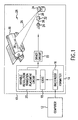
- Shown in Figure 2 is a simplified block diagram of logic 18 and an embodiment of variable resolution transition placement circuit 20.
- logic 18 includes an embodiment of a delayed clocks generator, such as delayed clocks circuit 100. Delayed clocks circuit 100 generates delayed versions of a system clock that are used to sample a reference signal, such as an nBD signal. The nBD signal is an inverted version of a beam detect signal (BD signal).
- phase measuring device 102 measures the phase difference between the rising edge of the system clock and the nBD signal.
- phase measuring device 102 An embodiment of phase measuring device 102 is disclosed in copending United States patent application serial number 09/534,747 (attorney's docket number 10990775), naming Robert D. Morrison and Eugene A. Roylance as inventors, assigned to Hewlett Packard Company, and incorporated by reference into this specification in its entirety.
- Variable resolution transition placement circuit 20 generates the video data using the system clock without using a video clock signal.
- the system clock signal is used elsewhere on formatter 14. For example, processing devices included within rasterizer 16 are clocked using the system clock.
- Generation of the video data using the system clock provides several advantages. Using the system clock for video data generation eliminates the requirement for the hardware to generate the video clock signal. In addition, using the system clock for video data generation removes the difficulty involved in passing data between two asynchronous clock domains.
- the timing of edges of a synthesized video clock are determined with respect to the system clock using the system clock.
- the synthesized video clock is not actually generated by the variable resolution transition placement circuit 20.
- the number of video clock cycles that would have occurred are computed for each system clock cycle to form the synthesized video clock.
- the time of one synthesized video clock period substantially equals the time during which pulsating beam 26 is swept across a dimension of an area on photoconductor drum 30 (in the direction of movement of pulsating beam 26 across photoconductor drum 30) corresponding to a width of a pixel.
- This dimension of the pixel will be referred to as a "pixel width”.
- the time period during which pulsating beam 26 sweeps a distance substantially equal to the pixel width will be referred to as a "pixel time period" and it corresponds in length to a single period of the synthesized video clock.
- the data supplied by rasterizer 16 to variable resolution transition placement circuit 20 specifying the positions of transitions (if any) during the pixel time period will be referred to as pixel data.
- a scan line is formed from a line of contiguous pixels across the surface of photoconductor drum 30 corresponding to a sweep of pulsating beam 26 across the surface of photoconductor drum 30.
- a left edge of a pixel corresponds to the edge of the pixel width first encountered as pulsating beam 26 sweeps across photoconductor drum 30.
- a right edge of a pixel corresponds to the edge of the pixel width last encountered as the pulsating beam 26 sweeps across photoconductor drum 30.
- Variable resolution transition placement circuit 20 includes a configuration that allows it to selectively vary the period of the synthesized video clock, pixel by pixel if desired. By varying the period of the synthesized video clock, variable resolution transition placement circuit 20 has the capability to vary the pixel width from pixel to pixel across the scan line.
- Logic 18 includes code generator 104.
- Pixel data received from rasterizer 16 by code generator 104 includes information indicating the number of transitions within a synthesized video clock period and the position of these transitions within the synthesized video clock period with respect to the beginning of the synthesized video clock period.
- the output of code generator 104 includes binary encoded values generated using the pixel data. These values specify the desired positions of transitions within the synthesized video clock period with respect to the beginning of the synthesized video clock.
- the pixel data supplied by rasterizer 16 can specify up to four transitions in each pixel. As will be disclosed in more detail later in this specification, with four transitions specified in a pixel one will occur at the left edge of the pixel and one will occur at the right edge of the pixel.
- Code generator 104 is configured so that when the pixel data specifies the generation of a transition at the right edge of the corresponding pixel, Code generator 104 will delay this transition so that it is placed at the left edge of the next pixel. Therefore, code generator 104 can generate a maximum of three binary encoded values specifying transitions within a pixel. If the pixel data for the next pixel also specifies a transition at the left edge of the next pixel, these transitions will cancel and code generator 104 will not generate a transition for either the right edge of the current pixel or the left edge of the next pixel.
- Hardware and firmware included in formatter 14 maintains a count indicating to which pixel the pixel data supplied by rasterizer 16 corresponds. Pixel data is supplied to variable resolution transition placement circuit 20 in correspondence to this count. That is, the pixel data corresponding to any given pixel in the sweep of pulsating beam 26 is supplied when the count corresponds that particular pixel. In addition, the pixel data for any given pixel is supplied to variable resolution transition placement circuit 20 the correct number of system clock cycles in advance so that the video data generated at the output of variable resolution transition placement circuit 20 for that pixel occurs when pulsating beam 26 is located at the correct position on that pixel. Supplying the pixel data in this manner accounts for the processing time required within variable resolution transition placement circuit 20.
- a conversion is done from the synthesized video clock domain to the system clock domain.
- This conversion translates transitions supplied by code generator 104 from the synthesized video clock domain to the system clock domain.
- This conversion operation is performed in an embodiment of a converter, converter 106.
- Converter 106 receives input from an embodiment of a transform generator, such synthesized video clock to system clock transfer function generator 108.
- Synthesized video clock to system clock transfer function generator 108 could be implemented using a processing device such as a digital signal processor.
- Synthesized video clock to system clock transfer function generator 108 generates a value that is the ratio between the system clock frequency and the synthesized video clock frequency for a particular system clock cycle.
- the value generated by synthesized video clock to system clock transfer function generator 108 can change depending upon the desired transfer function over a scan line.
- This transfer function could be selected to generate a relatively smooth variation in resolution across the scan line that compensates for the variable sweep rate of pulsating beam 26 across photoconductor drum 30 resulting from the absence of a flat focusing lens.
- this transfer function could be selected to generate a step change in resolution across the scan line that could, for example, be used to print pictures at one resolution and text at another resolution.
- this transfer function could be selected to scale an image so that an image having a lower resolution (generated by scanning a unit of media) than the nominal resolution of the imaging device would be generated at the same size as in the unit of media upon which printing was performed. Or, this transfer function could be selected to generate a substantially constant resolution across the scan line. In addition, this transfer function could be selected to achieve an arbitrary resolution versus displacement function over the scan line.
- the transfer function is not limited to a smoothly varying transfer function but can be any analytic transfer function, Even discretely varying functions have special utility in imaging devices. However, correctly representing a smoothly continuous frequency transfer function has unique implementation challenges discussed in the following paragraphs.
- the problem confronted is how to generate the value in synthesized video clock to system clock transfer function generator 108 for each system clock cycle so that the desired resolution transfer function is generated with sufficient accuracy.
- the ultimate measure of the accuracy is the accuracy with which transitions specified by the pixel data are placed within the corresponding pixel.
- the resolution transfer specifies a first synthesized video clock frequency at the left edge of a pixel and a second synthesized video clock frequency at the right edge of the pixel with a smooth variation between the left edge and the right edge.
- a single transition is to be placed within that pixel.
- the problem is how to determine the correct position of the transition, with respect to the system clock cycles, in a way that accounts for the variation in synthesized video clock frequency over the pixel.
- Determining the correct position of a transition effectively involves conversion between several domains. There is a conversion from the frequency domain to the time domain and then to the spatial domain to determine the transition position within the pixel. Then, there is a conversion from the spatial domain back to the time domain in determining the system clock cycle and the fractional portion of that system clock cycle at which the transition is to be generated.
- One way in which to approximately account for the synthesized video clock frequency variation across pixels is to use the ratio between the system clock frequency and the synthesized video clock frequency at the left edge of the pixel for all system clock cycles occurring during that pixel. Another approximation is to average the ratio at the left edge of the pixel and the right edge of the pixel and use this average ratio for all system clock cycles occurring during that pixel.
- the values of the synthesized video clock frequency at the left edge of a pixel and the right edge of the pixel are determined by the particular transfer function selected for use in synthesized video clock to system clock transfer function generator 108.
- the transfer function selected depends upon the effect that it is desired to achieve over the scan line.
- the transfer function used in synthesized video clock to system clock transfer function generator 108 has the effect of shifting, in a non-linear way, the incoming transitions specified with respect to the beginning of synthesized video clock cycles and specifying them with respect to the system clock domain.
- converter 106 uses the value received from synthesized video clock to system clock transfer function generator 108 to convert them from the synthesized video clock domain to the system clock domain.
- the unconverted binary encoded values represent the positions of the transitions within a cycle of the synthesized video clock in terms of a representation corresponding to fractional portions of a synthesized video clock cycle.
- the converted binary encoded values represent the positions of the transitions within a period, or possibly multiple periods of the system clock in terms of integer and fractional parts of system clock periods.
- the placement of the transitions may cross boundaries of system clock cycles depending upon the position of the transitions within the synthesized video clock period and depending upon the ratio of the system clock frequency to the synthesized video clock frequency for the particular cycle of the synthesized video clock for which the conversion is performed.
- the determination of which cycle of the system clock the transitions will be placed (accounting for the delay of transitions, if any delay occurs, between periods of the system clock) and where within the cycle, or cycles, of the system clock the transitions will be placed is determined in converter 106.
- the conversion performed by converter 106 includes determining the position, in terms of a fractional portion of the system clock period, from a beginning of a system clock cycle using the value received from the synthesized video clock to system clock transfer function generator 108 and computing the number of the system clock cycles into the future (relative to the current system clock cycle) in which the transition is to be generated.
- the integer portion of the values generated by converter 106 represent the number of the system clock cycles into the future, from the system clock cycle during which converter 106 generates the corresponding integer value, in which the transitions will be placed.
- the fractional portion of the values generated by converter 106 represent the position, with respect to the beginning of the corresponding system clock cycle in which the transitions will be placed, of the transition.
- the offset between the beginning of the system clock cycles in which the transitions are to be placed and the beginning of the corresponding synthesized video clock cycles is not taken into account.
- the values (including the integer and fractional portion) generated by converter 106 are added to other offsets computed (such as the offset between the beginning of system clock cycles and the corresponding synthesized video clock cycle) in different parts of the circuit (described later) to determine the system clock cycle and the position within the system clock cycle at which the transitions will be placed.
- An embodiment of a synthesized video generator such as synthesized video generator 109 generates values that represent an integer and fractional portion of the synthesized video clock position on system clock cycles.
- a transform generator such as system clock to synthesized video clock transfer function generator 110, generates a value that is the ratio between the synthesized video clock frequency and the system clock frequency for a system clock cycle.
- the values generated by system clock to synthesized video clock transfer function generator 110 are used to determine the position within synthesized video clock cycles at a beginning of system clock cycles.
- System clock to synthesized video clock transfer function generator 110 could be implemented using a processing device, such as a digital signal processor.
- variable resolution transition placement circuit 20 for a given transfer function selected for a scan line, the values generated in the synthesized video clock to system clock transfer function generator 108 and the system clock to synthesized video clock transfer function generator 110 will be, on a system clock cycle by system clock cycle basis, related to each other as reciprocals.
- a storage device such as current clock register 112 contains a value that represents the position of the synthesized video clock corresponding to the current cycle of the system clock.
- an adder such as adder 114, adds the value generated for that system clock cycle by system clock to synthesized video clock transfer function generator 110 to the value stored in current clock register 112 (which, prior to updating at the start of each system clock cycle, represents the value of the synthesized video clock for the previous cycle of the system clock) to determine the position, on the current cycle of the system clock, in the cycle of the synthesized video clock.
- the output of adder 114 is stored in current clock register 112.
- the value held in current clock register 112 includes bits that represent the integer portion and the fractional portion of the synthesized video clock.
- the number of bits required to represent the fractional part is influenced by the error that can be tolerated in the placement of transitions over the scan line.
- the value provided by system clock to synthesized video clock transfer function generator 110 would be exactly equal to the number of synthesized video clock cycles that occur with the passage of each system clock cycle. However, because this value is very likely (though not necessarily) an irrational number, an infinite number of bits would be required to exactly represent this value.
- the value provided by system clock to synthesized video clock transfer function generator 110 will introduce error in the computation of the synthesized video clock.
- the error in the synthesized video clock will lead to error in placement of the transitions over the scan line.
- the number of bits chosen to represent the fractional portion of the synthesized video clock value will be selected so that the worst case possible error over the scan line in the synthesized video clock will not result in an unacceptable error in placement of transitions.
- the error in the generation of the synthesized video clock results from the limited number of bits used to represent the fractional part of the value and round off error from successive additions in adder 114.
- To determine the worst possible error over the scan line it is assumed that the error in the generation of the synthesized video clock on each system clock cycle resulting from round off has the same sign. Therefore, the worst case error in the synthesized video clock will occur for the pixel at the end of the scan line.
- the number of bits used to represent the fractional portion of the synthesized video clock is selected so that the worst case error in the synthesized video clock value (along with sources of error contributed by other portions of variable resolution transition placement circuit 20) will not result in an error in the placement of the transitions greater than a predetermined level.
- variable resolution transition placement circuit 20 there are at most, approximately ten thousand additions required over a scan line.
- 22 bits are used (14 bits to achieve the 1/64th clock period error over, at most, ten thousand additions, 6 bits to represent the fractional part of the value maintained in current clock register 112, and 2 additional bits for margin).
- the number of bits used in the fractional part of the value in current clock register 112 is influenced by the desired accuracy in the placement resolution (in terms of fractions of the system clock) and the number of additions performed over the scan line. It should be emphasized that a different number of bits could be used to represent the fraction part of the value in current clock register 112. A lower level of desired accuracy and resolution would require fewer number of bits. A greater level of accuracy and resolution would require a greater number of bits.
- the value in current clock register 112 includes an integer portion. A change in the integer portion of this value between system clock cycles is used to determine if a boundary between successive cycles of the synthesized video clock has been crossed.
- the number of bits used to represent the integer portion of the value in current clock register 112 is related to the number of synthesized video clock cycles into the future that are concurrently scheduled. In an embodiment of variable resolution transition placement circuit 20, transitions for the next 3 cycles of the synthesized video clock are scheduled. To designate these 3 cycles of the synthesized video clock, 2 bits are used for the integer portion of the value in current clock register 112. Therefore, in this embodiment, 24 bits are used for the integer and fractional part of the value in current clock register 112. A greater or fewer number of bits would be used for the integer portion to schedule transitions for, correspondingly, a greater or fewer number future cycles of the synthesized video clock.
- next clock register 116 maintains a running count of a value that is used to represent the synthesized video clock corresponding to the next cycle of the system clock.
- Next clock register 116 is coupled to the output of a adder 118 and current clock register 112. After the value in current clock register 112 has been updated at the beginning of the current system clock cycle, adder 118 adds the value generated by system clock to synthesized video clock transfer function generator 110 to the value in current clock at the beginning of the next system clock cycle.
- the difference between the values in current clock register 112 and next clock register 116 is equal to the value provided by system clock to synthesized video clock transfer function generator 110 for that system clock cycle over the cycles of the system clock. Because the value generated by system clock to synthesized video clock transfer function generator 110 can change between system clock cycles, the difference between the values stored in current clock register 112 and next clock register 116 can change between system clock cycles.
- the values in current clock register 112 and next clock register 116 are updated at the beginning of the system clock cycle. However, the values in current clock register 112 and next clock register 116 represent the synthesized video clock on different cycles of the system clock.
- the value in next clock register 116 represents the synthesized video clock one system clock cycle later than the value in current clock register 112.
- variable resolution transition placement circuit 20 two bits are used to represent the integer portion of the value in current clock register 112 and next clock register 116. As the value in system clock to synthesized video clock transfer function generator 110 is added to values in these registers, the integer portion will exceed that which can be represented by two bits. The overflow bits from the addition are dropped. As a result, instead of representing the absolute value of the synthesized video clock, the values in current clock register 112 and next clock register 116 represent the synthesized video clock within several cycles of the synthesized video clock relative to a previous cycle of the system clock.
- the amount of hardware necessary to implement variable resolution transition placement circuit 20 is reduced. Fewer bits are required to represent the integer portion of the values in current clock register 112 and next clock register 116.
- the relative value of the synthesized video clock can be tracked through successive additions instead of determining the absolute value of the synthesized video clock at the beginning of each system clock cycle through multiplication.
- an absolute synthesized video clock value could be generated (at the expense of increased hardware complexity) at the beginning of each system clock cycle. This could be accomplished, for example, by including a sufficient number of bits in current clock register 112 and next clock register 116 for the integer portion to store the total number of synthesized video clock cycles that occur over a scan line. Then, after each addition of the value from the system clock to synthesized video clock transfer function generator 110 for that system clock cycle, the resulting value corresponds to the absolute value of the synthesized video clock.
- the values in current clock register 112 and next clock register 116 are used to determine when the boundary between successive synthesized video clock cycles will be crossed. As will be discussed in more detail later, in some situations, placement of transitions at the proper position within a cycle of the synthesized video clock involves anticipating that the boundary between successive synthesized video clock cycles will be crossed before the beginning of the next system clock cycle.
- the values in current clock register 112 and next clock register 116 are also used to generate a valid signal used to indicate whether values of transition positions generated by other parts of variable resolution transition placement circuit 20 correspond to valid transitions.
- the valid signal is used by other parts of variable resolution transition placement circuit 20 to determine the value of valid bits associated with transition values that are generated.
- the valid signal is used to control the flow of pixel data from rasterizer 16 to code generator 104.
- Integer comparison block 120 is used to compare the integer portion of the values stored in current clock register 112 and next clock register 116. This comparison is performed on each system clock cycle. By comparing the integer portion of the values in current clock register 112 and next clock register 116, a determination can be made of the system clock cycle during which the synthesized video clock crosses the boundary between successive system clock cycles. When the integer portions of the value in current clock register 112 and next clock register 116 are equal, this indicates that the beginning of the system clock cycles corresponding to the values in current clock register 112 and next clock register 116 occur during the same cycle of the synthesized video clock.
- the valid signal is set to a state indicating that valid transition data will be generated by the other parts of variable resolution transition placement circuit 20.
- the state of the valid signal indicates to rasterizer 16 that pixel data for the pixel corresponding to the next cycle of the synthesized video clock should be sent to code generator 104.
- Transitions are scheduled for placement in a future synthesized video clock cycle at the beginning of a system clock cycle prior to the beginning of the synthesized video clock during which the transitions are to occur. Scheduling is done in this manner so that the transition positions are available to variable resolution transition placement circuit 20 before the beginning of the synthesized video clock cycle during which they are to occur.
- the scheduling of transitions is performed so that transitions for the next two successive cycles of the synthesized video clock that are to occur are scheduled. As synthesized video clock cycles occur and the scheduled transitions for those synthesized video clock cycle are generated, transitions for future cycles of the synthesized video clock are scheduled so that transitions for the next two successive cycles of the synthesized video clock are concurrently scheduled.
- variable resolution transition placement device 20 includes the capability to generate up to four transitions during a synthesized video clock cycle.
- a maximum of six transitions could be scheduled because transitions specified to occur at the right edge of a pixel will be placed at the left edge of the next pixel (thus only permitting three actual transitions in the current pixel, meaning that a maximum of six transitions can be scheduled in two pixels).
- Six transitions would be scheduled when the next two successive cycles of the synthesized video clock will each include four transitions (in which case transitions at the right edge of pixel will be moved to the left edge of the next pixel and thereby cancel the transition specified to occur at the left edge of the next pixel).
- Sufficient storage capacity is included in this embodiment of variable resolution transition placement circuit 20 to hold the data used for generating the scheduled transitions.
- transitions are scheduled for two cycles of the synthesized video clock to ensure that data will be available for generating transitions at the proper time.
- one or more transitions are located near the end of a synthesized video clock cycle and one or more transitions are located near the beginning of the next synthesized video clock cycle. With this situation, it is possible that transitions existing within two cycles of the synthesized video clock need to be generated within the cycle of the system clock that includes the boundary between successive cycles of the synthesized video clock.
- phase difference between the beginning of the synthesized video clock cycle and the system clock cycle may result in the shifting of transitions from the future cycles of the system clock into a system clock cycle in which transitions from the current cycle of the synthesized video clock are to be placed.
- phase difference between the system clock and the nBD signal results in the shifting of transitions between cycles of the system clock. Therefore, to ensure that the data is available for generating transitions at the desired positions under these circumstances, transitions for two successive synthesized video clock cycles into the future are scheduled.
- Converter 122 converts the fractional part of the value stored in next clock register 116 into a position within the corresponding cycle of the synthesized video clock in terms of 1/32 time increments of a system clock cycle relative to the beginning of the corresponding cycle of the system clock.
- the value generated by converter 122 is used to account for the offset between the beginning of a system clock cycle and the beginning of the corresponding synthesized video clock cycle in determining the correct position for placement of transitions relative to the beginning of system clock cycles.
- the fractional portion of the value in next clock register 116 at the beginning of each system clock cycle represents the offset from the beginning of the synthesized video clock cycle in which the system clock cycle occurs to the beginning of that cycle of the system clock. The value of this offset increases as successive cycles of the system clock occur during that cycle of the synthesized video clock.
- Converter 122 performs a multiplication on the fractional portion of the value stored in next clock register 116. This multiplication converts the fractional portion of a synthesized video clock cycle into a corresponding value expressed as the number of 1/32's of a system clock cycle of offset between the beginning of the synthesized video clock cycle and the beginning of the next occurring system clock cycle.
- the offset is computed for every system clock cycle within the synthesized video clock cycle.
- the multiplication performed by converter 122 includes multiplying the fractional value stored in next clock register 116 by value stored in synthesized video clock to system clock transfer function generator 108 for every system clock cycle.
- the resulting value which may include an integer portion as well as a fractional portion, represents the offset.
- the integer portion is the number of system clock cycles of offset and fractional portion is the phase offset within a cycle of the system clock.
- An adding device such as adder 124 performs a signed addition of five types of values supplied by other portions of variable resolution transition placement circuit 20.
- the first value is the phase difference value generated by phase measuring device 102 is supplied to adder 124.
- the phase difference is represented as the number of time increments between successive outputs of delayed clocks circuit 100 most closely corresponding to the time between the beginning of the system clock cycle closest in time to the active edge of the nBD signal.
- the phase difference is a positive value.
- the second value supplied to adder 124 includes the values generated by converter 106.
- code generator 104 generates three binary encoded values. If there are three transitions in the corresponding pixel, all of these binary encoded values will be valid.
- Converter 106 generates three values from the three values supplied by code generator 104.
- Adder 124 includes 3 adders in a parallel configuration. Each of the three adders adds one of the three values received from converter 106 to one of the other four values supplied to adder 124.
- Each of the three values generated by converter 106 includes an integer portion (representing the number of the system clock cycle in the future during which the corresponding transition occurs) and a fractional portion (representing the fraction of the system clock cycle at which the corresponding transition occurs).
- each of the values supplied by converter 106 is a positive value.
- the input provided to adder 124 labeled "R" represents a rounding value.
- the rounding value used in one implementation of variable resolution transition placement circuit 20 is one half of the value of the lowest order bit of the values generated by adder 124. For example, if the fractional portion of the values generated by adder 124 specify the position of the transitions at 1/32 of a system clock cycle resolution, one half of the lowest order bit would correspond to binary value .000001 (base 2).
- the input provided to adder 124 labeled "E” represents a dithering value used to slightly shift the position of the transition, either forward or back in time, in a random fashion from transition to transition for the purposes of controlling radiated emissions.
- the radiated energy that would have been present at the frequency corresponding to the repetitive occurrence of those transitions at substantially the same positions within system clock cycles is spread over a range of frequencies. This allows compliance with product radiated emission requirements to be more easily achieved.
- the output generated by adder 124 is utilized by an embodiment of a transition queuing device, such as transition queue 126 to store information specifying the position of transitions for the next two cycles of the synthesized video clock.
- the values provided by adder 124 each include an integer portion and a fractional portion.
- the integer portion specifies the system clock cycle into the future in which a transition is to occur and the fractional portion specifies where within that system clock cycle the transition is to occur.
- the system clock cycle into the future in which the transition is to occur is specified relative to the time at which integer portion is stored in transition queue 126.
- Transition queue 126 includes a configuration for storing the integer portion and the fractional portion of each of the values supplied by adder 124.
- the integer value specifying the system clock cycle in which each of the scheduled transitions are to be placed is decremented within transition queue 126.
- the ratio of the system clock frequency to the synthesized video clock frequency is such that at the time converter 106 determines the cycles of the system clock during which the transitions will be placed, those transitions will be placed, respectively one and five system clock cycles into the future.
- the integer values specifying the future system clock cycles in which each of the transitions will be placed are, respectively, one and five. At the beginning of each system clock cycle, these integer values are decremented.
- Transition generation logic 128 includes transition data generator 130 and transition logic 132.
- Transition data generator 130 uses the code or codes received from transition queue 126 to generate the transition data value.
- Transition logic 132 receives the transition data value.
- Transition logic 132 includes the hardware necessary to generate the video data stream having transitions at positions specified by the pixel data supplied to variable resolution transition placement circuit 20.
- An embodiment of transition generation logic 128 that would be suitable for use within variable resolution transition placement circuit 20 is disclosed in copending United States patent application serial number 09/534,747, previously incorporated by reference in its entirety.
- Transition queue 126 includes an embodiment of a transition queuing control device, transition queuing control 200.
- Transition queuing control 200 includes a configuration to manage the scheduling of transitions.
- Transition queuing control 200 receives, for each transition to be scheduled, the output from adder 124 specifying the future system clock cycle in which the transition is to occur and the position of the transition within that system clock cycle.
- the position of the transition within the system clock cycle is encoded within the fractional portion of the values received from adder 124.
- variable resolution transition placement circuit 20 the frequency of the system clock was assumed to be greater than that of the synthesized video clock. It should be recognized that embodiments of variable resolution transition placement circuit 20 for which the frequency of the synthesized video clock frequency is greater than the system clock frequency are possible. For these embodiments, multiple groups of the binary encoded values specifying transition positions for a pixel would be supplied on each system clock cycle. In addition, without an increase number of delay taps provided in the delayed clocks circuit, the placement resolution within a cycle of the synthesized video clock would drop.
- the encoding represents the output of a delayed clocks circuits similarly for other resolutions, such as 1/16 or 1/64 of a system clock cycle. It should be recognized that this encoding from fractional value to tap number works when the number of taps is an integer power of two. However, when the number of taps is non-integer power of two, this encoding scheme will not be applicable. In that case, a translation circuit that receives the fractional part as an input and converts it to a tap number would be used.
- transition queuing control 200 determines that one or more counter values have reached zero, the corresponding fractional portions for the transition or transitions having valid bits in an asserted state are decoded and sent to the transition generation logic 128 at the beginning of the next system clock cycle.
- Decoding the fractional portion involves forming a binary encoded value by assigning the bits as non-negative coefficients of two as previously specified.
- transition generation logic 128 uses the binary coded values, transition generation logic 128 generates the specified transitions at the desired time within the video data stream. The number of bits needed to represent the value specifying the system clock cycle numbers during which transitions will occur depends upon the maximum ratio of the system clock frequency to the synthesized video clock frequency.
- a pixel data byte is supplied to the input of code generator 104 synchronous with the beginning of the system clock.
- Each pixel data byte defines the pulse shape and pulse width for the corresponding pixel.
- the term "pulse width” refers to the total fraction (realizing that non-contiguous portions within a single pixel can be exposed) of the pixel in the direction pulsating beam 26 is swept which is to be exposed by pulsating beam 26.
- the term "pulse shape” refers to the relative positioning of the exposed regions within the pixel.
- variable resolution transition placement device permits a left justified pulse, a right justified pulse, a center justified pulse or a split justified pulse.
- four pulse shapes are permitted in this embodiment, it should be recognized that with a different number of bits used a larger or smaller number of pulse shapes could be defined. For a larger number of possible pulse shapes, more bits would be required to define the desired pulse shape.
- the pulse shape and pulse width are encoded in the pixel data byte.
- the two highest order bits of the pixel data byte are used to specify generation of one of four pulse shapes.
- the left justified pulse is defined by two transitions in the pixel. The first transition is located at the left edge of the pixel and the second transition is located within the pixel at a position determined from the lower order five bits.
- the center justified pulse is defined by two transitions within the pixel. The positions of the transitions are determined from the lower order five bits.
- the right justified pulse is defined by two transitions in the pixel. The first transition is located within the pixel at a position determined from the lower order five bits. The second transition is located at the right edge of the pixel.
- the split justified pulse is defined by four transitions in the pixel. One transition is located on the left edge of the pixel and one transition is located on the right edge of the pixel. The remaining two transitions are located within the pixel at positions determined from the lower order five bits.
- Converter 106 receives the binary encoded values from code generator 104 and the value from synthesized video clock to system clock transfer function generator 108.
- the binary encoded values from code generator 104 specify transition positions within and relative to the beginning of synthesized video clock cycles.
- Converter 106 converts the binary encoded values from the synthesized video clock domain to the system clock domain.
- an embodiment of code generator 104 can generate binary encoded values corresponding to four pulse shapes.
- Three of the pulse shapes include at least one transition at either the beginning or end of a synthesized video clock pulse.
- the position of at least one of the transitions (and maybe two of the transitions) in the pulse shape, in terms of fractional portions of a system clock cycle will be zero because the transition or transitions will be located on either or both of the left edge or the right edge of the synthesized video clock. For these transitions, no computation is required in converter 106.
- the binary encoded values generated by an embodiment of code generator 104 specify the position of the transitions within a synthesized video clock cycle expressed as a fraction of a synthesized video clock cycle. For example, a transition located at 26/32 of a synthesized video clock cycle would correspond to a binary encoded value of 11010. For a transition located at the left edge of a synthesized video clock cycle (0/32), the corresponding binary encoded value would be 00000. A transition located at the right edge of a synthesized video clock cycle (32/32), is moved to the left edge of the next pixel by code generator 104. Therefore, for transitions specified by code generator 104 to be placed at the left edge of the current pixel or the left edge of the next pixel, no multiplication is required because the result will zero.
- Converter 106 includes input registers 200-202 for storing the binary encoded values provided by code generator 104.
- the binary encoded value for transitions located between the left edge of the pixel and the center of the pixel is stored in left register 200.
- the binary encoded value for transitions located between the center of the pixel and the right edge of the pixel is stored in right register 202.
- Zero register 204 is the register for the binary encoded value corresponding to a transition placed at the left edge of the pixel. Because the binary encoded value in zero register 204 will always be zero, a single valid bit could be used for this value.
- Associated with each of the registers 200-204 are valid bits V0-V2 also generated by code generator 104.
- Converter 106 also includes multiplier 208 and multiplier 210. Multiplier 208 and multiplier 210 each receive the value provided by synthesized video clock to system clock transfer function generator 108 for each synthesized video clock cycle. Multiplier 208 and multiplier 210 multiply the value provided by synthesized video clock to system clock transfer function generator 108 by, respectively, the values in input register 200 and input register 202.
- the result, along with the corresponding valid bits V0-V1 are supplied at the output of converter 106.
- the value in zero register 204 corresponds to the transition (if there is one) placed at the left edge of the pixel. Since the binary encoded value in input register 204 will be zero, no multiplication is required for this value. Accordingly, this value is passed through without multiplication along with valid bit V2.
- Converter 122 includes multiplier 300 to receive the fractional portion of the value in next clock register 116 and to receive the value generated by synthesized video clock to system clock transfer function generator 108. Multiplier 300 multiplies these two values on each system clock cycle to generate the offset between the beginning of the synthesized video clock cycle and that system clock cycle.
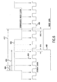
- Shown in Figure 6 is a diagram illustrating a timing relationship between a system clock waveform 400 and the synthesized video clock waveform 402 that would result if it were actually generated.
- Synthesized video clock waveform 402 is shown as a dashed line to emphasize that it is a virtual waveform. That is, synthesized video clock waveform 402 is not actually generated. Rather, the position of synthesized video clock waveform is computed for each system clock cycle.
- the frequency of system clock waveform 400 is shown as greater than the frequency of synthesized video clock waveform 402, as previously mentioned, the opposite could be true.
- the arrows, of which arrow 404 is exemplary correspond to the positions at which values of synthesized video clock waveform 402 are computed.
- An offset 406 (the value of which is computed by converter 122) between the beginning of a synthesized video clock cycle and the beginning of a system clock cycle is also shown in Figure 6.
- Video data waveform 408 for a single pixel corresponds to the generation of a center justified pulse.
- the left edge of the center justified pulse occurs a time interval 410 after the left edge of the synthesized video clock.
- the right edge of the center justified pulse occurs a time interval 412 after the left edge of the synthesized video clock.
- the position of the left edge and right edge of the center justified pulse with respect to the beginning of system clock cycles are shown by, respectively time interval 414 and time interval 416.
- FIG. 7 Shown in Figure 7 is a high level flow diagram for using an embodiment of the variable resolution transition placement circuit 20 to generate a transition.
- code generator 104 generates binary encoded values using pixel data received from rasterizer 16. These binary encoded values represent the positions of transitions relative to the beginning of a cycle of the synthesized video clock.
- converter 106 converts these binary encoded values to transition positions relative to the system clock.
- converter 122 computes an offset between the beginning of a synthesized video clock cycle and a system clock cycle.
- adder 124 combines the transition positions, the offset and a phase difference previously determined by phase measuring device 102 to determine shifted transition positions and stores the shifted transition positions in transition queue 126.
- transition generation logic 128 generates the transitions after receiving the shifted transition positions on the correct cycle of the system clock.
- variable resolution transition placement device has been illustrated, and described, it is readily apparent to those of ordinary skill in the art that various modifications may be made to this embodiment without departing from the scope of the appended claims.
Landscapes
- Engineering & Computer Science (AREA)
- Physics & Mathematics (AREA)
- General Physics & Mathematics (AREA)
- Signal Processing (AREA)
- Optics & Photonics (AREA)
- General Engineering & Computer Science (AREA)
- Multimedia (AREA)
- Theoretical Computer Science (AREA)
- Laser Beam Printer (AREA)
- Fax Reproducing Arrangements (AREA)
- Facsimile Scanning Arrangements (AREA)
- Analogue/Digital Conversion (AREA)
- Editing Of Facsimile Originals (AREA)
Abstract
Description
Claims (10)
- In an imaging device (10), a method for generating a transition, comprising:converting (502) a first position of the transition relative to a synthesized clock (402) to a second position of the transition relative to a clock (400);determining (504) an offset between the synthesized clock (402) and the clock (400);shifting (506) the second position based upon the offset and a phase difference between the clock and a reference signal to form a shifted position; andgenerating (508) the transition at the shifted position.
- The method as recited in claim 1, wherein:converting (502) the first position includes multiplying the first position by a selectively variable transform value relating the clock (400) to the synthesized clock (402) for each cycle of the synthesized clock (402).
- The method as recited in claim 2, wherein:shifting (506) the second position includes subtracting the offset from the second position and adding the phase difference to the second position.
- The method as recited in claim 3, wherein:the synthesized clock (402) corresponds to a synthesized video clock (402);the clock (400) corresponds to a system clock (400);the reference signal corresponds to a beam detect signal; andthe transform value substantially equals a ratio of a frequency of the system clock (400) to a frequency of the synthesized video clock (402).
- A variable resolution transition placement device (20), comprising:a transform generator (108) to generate a selectively variable transform value;a first converter (106) to determine a first position of a transition relative to a clock (400) using a second position of the transition relative to a synthesized clock (402) and using the transform value;a synthesized clock generator (109) configured to generate a synthesized clock value;a second converter (122) configured to generate an offset value using the synthesized clock value;an adder (124) to combine the first position, the offset value, and a phase difference value to determine a cycle of the clock (400) and a third position within the cycle of the clock (400) to place the transition; anda transition queuing device (126) to store and output the third position according to the cycle of the clock determined.
- The variable resolution transition placement device (20) as recited in claim 5, wherein:the transform generator (108) includes a configuration to generate the transform value as a ratio of a frequency of the clock (400) and a frequency of the synthesized clock (402);with the cycle of the clock (400) corresponding to a first cycle, the transform generator (108) includes a configuration to generate the transform value for a second cycle of the clock (400) according to the frequency of the synthesized clock (402) determined for the second cycle of the clock (400);a value corresponds to the second position and defines the transition relative to a beginning of a corresponding cycle of the synthesized clock (402); andthe first converter (106) includes a configuration to determine the first position by multiplying the value by the transform value.
- The variable resolution transition placement device (20) as recited in claim 6, wherein:an integer value represents the first cycle of the clock (400) in which to place the transition and a fractional value represents the third position; andthe transition queuing device (126) includes a configuration decrement the integer value and output the fractional value when the integer value equals zero.
- An imaging device (10), comprising:a photoconductor (30);a rasterizer (16) configured to generate pixel data;a code generator (104) to generate a binary encoded value corresponding to a position of a transition relative to a synthesized clock (402) using the pixel data;a variable resolution transition placement device (20) including a transform generator (108) to generate a selectively variable transform value, a first converter (106) to determine the position of the transition relative to a system clock (400) using the binary encoded value and the transform value, a synthesized clock generator (109) configured to generate a synthesized clock value, a second converter (122) configured to generate an offset value using the synthesized clock value, an adder to combine the position of the transition relative to the system clock (400), the offset value, and a phase difference value to determine a cycle of the system clock (400) and an adjusted position within the cycle to place the transition, and a transition queuing device (126) to store and output the adjusted position according to the cycle determined;transition generation logic (128) to generate the transition according to the adjusted position; anda photoconductor (28) exposure system configured to expose the photoconductor (30) to light according to the transition.
- The imaging device (10) as recited in claim 8, further comprising:a phase measuring device (102) configured to generate the phase difference value according to a time difference between a beginning of a cycle of the system clock (400) and a transition of a beam detect signal; anda delayed clocks circuit (100) to generate a plurality of delayed system clocks for the phase measuring device (102) and the transition generation logic (128).
- The imaging device (10) as recited in claim 20, wherein:the transform generator (108) includes a configuration to generate the transform value as a ratio of a frequency of the system clock (400) and a frequency of the synthesized clock (402); andwith the cycle of the system clock (400) corresponding to a first cycle, the transform generator (108) includes a configuration to generate the transform value for a second cycle of the system clock (400) according to the frequency of the synthesized clock (402) determined for the second cycle of the system clock (400).
Applications Claiming Priority (2)
| Application Number | Priority Date | Filing Date | Title |
|---|---|---|---|
| US635177 | 1984-07-27 | ||
| US09/635,177 US6373515B1 (en) | 2000-08-09 | 2000-08-09 | Variable resolution transition placement device |
Publications (2)
| Publication Number | Publication Date |
|---|---|
| EP1179804A2 true EP1179804A2 (en) | 2002-02-13 |
| EP1179804A3 EP1179804A3 (en) | 2004-01-07 |
Family
ID=24546759
Family Applications (1)
| Application Number | Title | Priority Date | Filing Date |
|---|---|---|---|
| EP01306638A Withdrawn EP1179804A3 (en) | 2000-08-09 | 2001-08-02 | Transition placement in an electrophotographic device |
Country Status (3)
| Country | Link |
|---|---|
| US (1) | US6373515B1 (en) |
| EP (1) | EP1179804A3 (en) |
| JP (1) | JP2002154237A (en) |
Families Citing this family (6)
| Publication number | Priority date | Publication date | Assignee | Title |
|---|---|---|---|---|
| WO2001064642A2 (en) * | 2000-02-29 | 2001-09-07 | Cor Therapeutics, Inc. | Benzamides and related inhibitors of factor xa |
| US6839366B1 (en) * | 2001-08-29 | 2005-01-04 | Cisco Technology, Inc. | Laser frequency control using dithered control signal |
| US20040145647A1 (en) * | 2003-01-23 | 2004-07-29 | Morrison Robert D | Nonlinear transformation of pixel width |
| US7061519B2 (en) * | 2003-08-09 | 2006-06-13 | Hewlett-Packard Development Company, L.P. | Scaling an image |
| US7639407B2 (en) * | 2004-03-24 | 2009-12-29 | Lexmark International, Inc. | Systems for performing laser beam linearity correction and algorithms and methods for generating linearity correction tables from data stored in an optical scanner |
| US7941284B1 (en) * | 2008-03-03 | 2011-05-10 | Brooks Instrument, Llc | Systems, apparatuses, and methods for measuring a fluid characteristic using a coriolis flow meter |
Family Cites Families (9)
| Publication number | Priority date | Publication date | Assignee | Title |
|---|---|---|---|---|
| US4692877A (en) * | 1986-06-27 | 1987-09-08 | Ibm Corporation | Digital timing control system with memory look ahead |
| US5212716A (en) | 1991-02-05 | 1993-05-18 | International Business Machines Corporation | Data edge phase sorting circuits |
| US5477330A (en) | 1992-10-16 | 1995-12-19 | Printware, Inc. | Synchronization to a start-of-scan detection, and digital generation of variable frequencies, from a fixed-frequency fixed-phase frequency source in an image generator in order to highly accurately time the placement of pixels upon a scan line |
| US5438353A (en) | 1992-11-02 | 1995-08-01 | Hewlett-Packard Company | Clock signal generator for electrophotographic printers |
| US5963243A (en) * | 1993-11-10 | 1999-10-05 | Kabushiki Kaisha Tec | Exposing device for correcting an fθ error of a rotatable polygon mirror without using an fθ lens |
| US5760816A (en) | 1996-02-06 | 1998-06-02 | Hewlett-Packard Company | Variable phase clock generator for an electrophotographic printer |
| US5793709A (en) | 1996-04-19 | 1998-08-11 | Xli Corporation | Free loop interval timer and modulator |
| US5990923A (en) | 1997-11-14 | 1999-11-23 | Hewlett-Packard Company | High resolution dynamic pulse width modulation |
| US6259467B1 (en) * | 1999-02-09 | 2001-07-10 | International Business Machines Corporation | Multi stage oscillator phase alignment scheme |
-
2000
- 2000-08-09 US US09/635,177 patent/US6373515B1/en not_active Expired - Fee Related
-
2001
- 2001-08-02 EP EP01306638A patent/EP1179804A3/en not_active Withdrawn
- 2001-08-08 JP JP2001240278A patent/JP2002154237A/en active Pending
Also Published As
| Publication number | Publication date |
|---|---|
| EP1179804A3 (en) | 2004-01-07 |
| JP2002154237A (en) | 2002-05-28 |
| US6373515B1 (en) | 2002-04-16 |
Similar Documents
| Publication | Publication Date | Title |
|---|---|---|
| JP3534263B2 (en) | Image registration system | |
| JP2583717B2 (en) | Display device with fine position designation | |
| CA2128859C (en) | Halftoning in a hyperacuity printer | |
| JP4916125B2 (en) | Pixel clock generation apparatus, pulse modulation apparatus, and image forming apparatus | |
| US5124802A (en) | Electrostatic lasar printer with a short side length of a modulation area formed by pulse width modulation set relative to a detected toner particle size | |
| EP0685960A2 (en) | Rotating non-rotationally symmetrical halftone dots for encoding embedded data in a hyperacuity printer | |
| JPH07236059A (en) | Supersensitive printing system | |
| US7003241B1 (en) | Image recording device and an image recording system | |
| US20050275713A1 (en) | Synchronization signal generator and image forming apparatus | |
| CA2128841C (en) | Interlace formatting in a hyperacuity printer | |
| US6373515B1 (en) | Variable resolution transition placement device | |
| US6366307B1 (en) | Clock independent pulse width modulation | |
| EP0463879B1 (en) | Switching video signals | |
| US8086059B2 (en) | Sub-raster registration using non-redundant overwriting | |
| JP2897599B2 (en) | Image forming device | |
| US5638110A (en) | Two dimensional slope thresholding in a hyperacuity printer | |
| EP0893780A2 (en) | Method for resolution conversion of print data for a printer | |
| US6236427B1 (en) | Edge placement device | |
| EP0700196B1 (en) | Method and apparatus for image scaling using parallel incremental interpolation | |
| US7061519B2 (en) | Scaling an image | |
| JPH05308497A (en) | Image forming device | |
| EP1136272A2 (en) | Apparatus for and method of recording image | |
| US6340986B1 (en) | Method and device for time shifting transitions in an imaging device | |
| JP4817334B2 (en) | Method and apparatus for forming an image | |
| JP4136796B2 (en) | Frequency modulator |
Legal Events
| Date | Code | Title | Description |
|---|---|---|---|
| PUAI | Public reference made under article 153(3) epc to a published international application that has entered the european phase |
Free format text: ORIGINAL CODE: 0009012 |
|
| AK | Designated contracting states |
Kind code of ref document: A2 Designated state(s): AT BE CH CY DE DK ES FI FR GB GR IE IT LI LU MC NL PT SE TR |
|
| AX | Request for extension of the european patent |
Free format text: AL;LT;LV;MK;RO;SI |
|
| PUAL | Search report despatched |
Free format text: ORIGINAL CODE: 0009013 |
|
| RIC1 | Information provided on ipc code assigned before grant |
Ipc: 7H 04N 1/053 B Ipc: 7B 41J 2/44 B Ipc: 7G 06K 15/12 A |
|
| AK | Designated contracting states |
Kind code of ref document: A3 Designated state(s): AT BE CH CY DE DK ES FI FR GB GR IE IT LI LU MC NL PT SE TR |
|
| AX | Request for extension of the european patent |
Extension state: AL LT LV MK RO SI |
|
| 17P | Request for examination filed |
Effective date: 20040621 |
|
| AKX | Designation fees paid |
Designated state(s): DE GB IT |
|
| 17Q | First examination report despatched |
Effective date: 20061116 |
|
| GRAP | Despatch of communication of intention to grant a patent |
Free format text: ORIGINAL CODE: EPIDOSNIGR1 |
|
| STAA | Information on the status of an ep patent application or granted ep patent |
Free format text: STATUS: THE APPLICATION IS DEEMED TO BE WITHDRAWN |
|
| 18D | Application deemed to be withdrawn |
Effective date: 20090211 |