EP1179614A2 - Mandrel for electroforming orifice plates - Google Patents
Mandrel for electroforming orifice plates Download PDFInfo
- Publication number
- EP1179614A2 EP1179614A2 EP01306613A EP01306613A EP1179614A2 EP 1179614 A2 EP1179614 A2 EP 1179614A2 EP 01306613 A EP01306613 A EP 01306613A EP 01306613 A EP01306613 A EP 01306613A EP 1179614 A2 EP1179614 A2 EP 1179614A2
- Authority
- EP
- European Patent Office
- Prior art keywords
- orifice
- electroforming
- mandrel
- orifice plate
- orifice area
- Prior art date
- Legal status (The legal status is an assumption and is not a legal conclusion. Google has not performed a legal analysis and makes no representation as to the accuracy of the status listed.)
- Withdrawn
Links
Images



Classifications
-
- B—PERFORMING OPERATIONS; TRANSPORTING
- B41—PRINTING; LINING MACHINES; TYPEWRITERS; STAMPS
- B41J—TYPEWRITERS; SELECTIVE PRINTING MECHANISMS, i.e. MECHANISMS PRINTING OTHERWISE THAN FROM A FORME; CORRECTION OF TYPOGRAPHICAL ERRORS
- B41J2/00—Typewriters or selective printing mechanisms characterised by the printing or marking process for which they are designed
- B41J2/005—Typewriters or selective printing mechanisms characterised by the printing or marking process for which they are designed characterised by bringing liquid or particles selectively into contact with a printing material
- B41J2/01—Ink jet
- B41J2/135—Nozzles
- B41J2/16—Production of nozzles
- B41J2/1621—Manufacturing processes
- B41J2/1626—Manufacturing processes etching
-
- B—PERFORMING OPERATIONS; TRANSPORTING
- B41—PRINTING; LINING MACHINES; TYPEWRITERS; STAMPS
- B41J—TYPEWRITERS; SELECTIVE PRINTING MECHANISMS, i.e. MECHANISMS PRINTING OTHERWISE THAN FROM A FORME; CORRECTION OF TYPOGRAPHICAL ERRORS
- B41J2/00—Typewriters or selective printing mechanisms characterised by the printing or marking process for which they are designed
- B41J2/005—Typewriters or selective printing mechanisms characterised by the printing or marking process for which they are designed characterised by bringing liquid or particles selectively into contact with a printing material
- B41J2/01—Ink jet
- B41J2/135—Nozzles
- B41J2/14—Structure thereof only for on-demand ink jet heads
- B41J2/1433—Structure of nozzle plates
-
- B—PERFORMING OPERATIONS; TRANSPORTING
- B41—PRINTING; LINING MACHINES; TYPEWRITERS; STAMPS
- B41J—TYPEWRITERS; SELECTIVE PRINTING MECHANISMS, i.e. MECHANISMS PRINTING OTHERWISE THAN FROM A FORME; CORRECTION OF TYPOGRAPHICAL ERRORS
- B41J2/00—Typewriters or selective printing mechanisms characterised by the printing or marking process for which they are designed
- B41J2/005—Typewriters or selective printing mechanisms characterised by the printing or marking process for which they are designed characterised by bringing liquid or particles selectively into contact with a printing material
- B41J2/01—Ink jet
- B41J2/135—Nozzles
- B41J2/16—Production of nozzles
- B41J2/162—Manufacturing of the nozzle plates
-
- B—PERFORMING OPERATIONS; TRANSPORTING
- B41—PRINTING; LINING MACHINES; TYPEWRITERS; STAMPS
- B41J—TYPEWRITERS; SELECTIVE PRINTING MECHANISMS, i.e. MECHANISMS PRINTING OTHERWISE THAN FROM A FORME; CORRECTION OF TYPOGRAPHICAL ERRORS
- B41J2/00—Typewriters or selective printing mechanisms characterised by the printing or marking process for which they are designed
- B41J2/005—Typewriters or selective printing mechanisms characterised by the printing or marking process for which they are designed characterised by bringing liquid or particles selectively into contact with a printing material
- B41J2/01—Ink jet
- B41J2/135—Nozzles
- B41J2/16—Production of nozzles
- B41J2/1621—Manufacturing processes
- B41J2/1625—Manufacturing processes electroforming
-
- B—PERFORMING OPERATIONS; TRANSPORTING
- B41—PRINTING; LINING MACHINES; TYPEWRITERS; STAMPS
- B41J—TYPEWRITERS; SELECTIVE PRINTING MECHANISMS, i.e. MECHANISMS PRINTING OTHERWISE THAN FROM A FORME; CORRECTION OF TYPOGRAPHICAL ERRORS
- B41J2/00—Typewriters or selective printing mechanisms characterised by the printing or marking process for which they are designed
- B41J2/005—Typewriters or selective printing mechanisms characterised by the printing or marking process for which they are designed characterised by bringing liquid or particles selectively into contact with a printing material
- B41J2/01—Ink jet
- B41J2/135—Nozzles
- B41J2/16—Production of nozzles
- B41J2/1621—Manufacturing processes
- B41J2/1637—Manufacturing processes molding
-
- B—PERFORMING OPERATIONS; TRANSPORTING
- B41—PRINTING; LINING MACHINES; TYPEWRITERS; STAMPS
- B41J—TYPEWRITERS; SELECTIVE PRINTING MECHANISMS, i.e. MECHANISMS PRINTING OTHERWISE THAN FROM A FORME; CORRECTION OF TYPOGRAPHICAL ERRORS
- B41J2/00—Typewriters or selective printing mechanisms characterised by the printing or marking process for which they are designed
- B41J2/005—Typewriters or selective printing mechanisms characterised by the printing or marking process for which they are designed characterised by bringing liquid or particles selectively into contact with a printing material
- B41J2/01—Ink jet
- B41J2/135—Nozzles
- B41J2/16—Production of nozzles
- B41J2/1621—Manufacturing processes
- B41J2/164—Manufacturing processes thin film formation
- B41J2/1643—Manufacturing processes thin film formation thin film formation by plating
-
- C—CHEMISTRY; METALLURGY
- C25—ELECTROLYTIC OR ELECTROPHORETIC PROCESSES; APPARATUS THEREFOR
- C25D—PROCESSES FOR THE ELECTROLYTIC OR ELECTROPHORETIC PRODUCTION OF COATINGS; ELECTROFORMING; APPARATUS THEREFOR
- C25D1/00—Electroforming
- C25D1/08—Perforated or foraminous objects, e.g. sieves
-
- C—CHEMISTRY; METALLURGY
- C25—ELECTROLYTIC OR ELECTROPHORETIC PROCESSES; APPARATUS THEREFOR
- C25D—PROCESSES FOR THE ELECTROLYTIC OR ELECTROPHORETIC PRODUCTION OF COATINGS; ELECTROFORMING; APPARATUS THEREFOR
- C25D1/00—Electroforming
- C25D1/10—Moulds; Masks; Masterforms
-
- B—PERFORMING OPERATIONS; TRANSPORTING
- B41—PRINTING; LINING MACHINES; TYPEWRITERS; STAMPS
- B41J—TYPEWRITERS; SELECTIVE PRINTING MECHANISMS, i.e. MECHANISMS PRINTING OTHERWISE THAN FROM A FORME; CORRECTION OF TYPOGRAPHICAL ERRORS
- B41J2/00—Typewriters or selective printing mechanisms characterised by the printing or marking process for which they are designed
- B41J2/005—Typewriters or selective printing mechanisms characterised by the printing or marking process for which they are designed characterised by bringing liquid or particles selectively into contact with a printing material
- B41J2/01—Ink jet
- B41J2/135—Nozzles
- B41J2/14—Structure thereof only for on-demand ink jet heads
- B41J2002/14475—Structure thereof only for on-demand ink jet heads characterised by nozzle shapes or number of orifices per chamber
-
- Y—GENERAL TAGGING OF NEW TECHNOLOGICAL DEVELOPMENTS; GENERAL TAGGING OF CROSS-SECTIONAL TECHNOLOGIES SPANNING OVER SEVERAL SECTIONS OF THE IPC; TECHNICAL SUBJECTS COVERED BY FORMER USPC CROSS-REFERENCE ART COLLECTIONS [XRACs] AND DIGESTS
- Y10—TECHNICAL SUBJECTS COVERED BY FORMER USPC
- Y10T—TECHNICAL SUBJECTS COVERED BY FORMER US CLASSIFICATION
- Y10T428/00—Stock material or miscellaneous articles
- Y10T428/12—All metal or with adjacent metals
- Y10T428/12361—All metal or with adjacent metals having aperture or cut
-
- Y—GENERAL TAGGING OF NEW TECHNOLOGICAL DEVELOPMENTS; GENERAL TAGGING OF CROSS-SECTIONAL TECHNOLOGIES SPANNING OVER SEVERAL SECTIONS OF THE IPC; TECHNICAL SUBJECTS COVERED BY FORMER USPC CROSS-REFERENCE ART COLLECTIONS [XRACs] AND DIGESTS
- Y10—TECHNICAL SUBJECTS COVERED BY FORMER USPC
- Y10T—TECHNICAL SUBJECTS COVERED BY FORMER US CLASSIFICATION
- Y10T428/00—Stock material or miscellaneous articles
- Y10T428/12—All metal or with adjacent metals
- Y10T428/12389—All metal or with adjacent metals having variation in thickness
Definitions
- This invention relates to a mandrel, a method of making the mandrel and orifice plates electroformed using the mandrel.
- the orifice plate that is formed has a thin orifice area surrounded by a thicker border. The thinner orifice area allows more orifices to be packed into a given area while the thicker border allows the orifice plate to withstand the rigors of manufacturing.
- a prior-art mandrel for electroforming orifice plates has a substrate of glass, plastic or a polished silicon wafer.
- a thin film layer of conductive material is deposited on this substrate.
- the conductive material is typically of chrome and stainless steel.
- a layer of dielectric is deposited on the conductive layer.
- This dielectric layer is of a nonconductive material such as silicon carbide. Patterns on the dielectric layer are lithographically formed using conventional masking, ultraviolet exposure and etching techniques to dimensionally define a molding surface for molding orifices in orifice plates.
- U.S. Patent 4,773,971 discloses a method of making such a mandrel.
- Orifice plates are formed on a mandrel in an electroforming process.
- the orifice plates thus formed are all on a single sheet. Breaking tabs that are also electroformed on the sheet defines the boundaries of each orifice plate.
- the sheet of orifice plates is attached to a mounting tape, for example, the Nitto Denko Elep Holder type V-8T available from Nitto Denko Corporation, Tokyo, Japan.
- the orifice plates are next singulated into individual orifice plates by breaking the sheet along the breaking tabs.
- the mounting tape holds the singulated orifice plates for further processing.
- a machine next picks and places each orifice plate over a corresponding printhead die on a wafer containing many such dies.
- each printhead consisting of a die and an orifice plate is singulated using dice sawing.
- Each complete pair of orifice plate and printhead die is then ready for attaching to a pen body to complete the fabrication of an ink-jet pen.
- This pen body typically contains an ink reservoir which supplies ink to the printhead.
- the orifice plates are subjected to considerably rough handling during the steps of singulation and attachment to the printhead dies.
- the orifice plates will have to be of a certain minimum thickness.
- the size of an orifice is directly proportional to the thickness of an orifice plate due to the electroforming process, the thicker the orifice plate, the larger will be the orifices.
- These larger orifices will mean that fewer orifices can be packed into a given area, thus limiting the orifice count and resolution of an orifice plate. It is therefore desirable to keep the orifice plate thin so as to allow more orifices to be packed into a given area, since the orifices will be relatively smaller. However, this desirability contradicts the requirement to keep the orifice plates sufficiently thick for reasons previously discussed.
- Prior art mandrels can only form orifice plates that are substantially uniformly thick. There is therefore the need for a new mandrel and method for electroforming orifice plates of a non-uniform thickness.
- a mandrel in one aspect of the present invention, has a metallic layer on a substrate.
- the metallic layer has a first molding surface that is electrically isolated from a second molding surface.
- the second molding surface is for substantially electroforming an orifice area of an orifice plate.
- the first molding surface is for substantially electroforming portions on the orifice plate that are thicker than the orifice area. These thicker portions are preferably portions that form a border around the orifice area.
- the mandrel also has means for electroforming orifices in the orifice area.
- the first molding surface is predominantly allowed to electroform the thicker portions without the second molding surface electroforming the orifice area. As the thicker portions build up, they electrically connect the first and the second molding surfaces to allow the second molding surface to subsequently electroform the orifice area.
- the orifice plate thus formed is non-uniformly thick.
- a preferred method of making the above mandrel involves depositing a metallic layer on a substrate followed by depositing a first photoresist layer on the metallic layer.
- a first photomask having a first pattern is positioned on the first photoresist layer.
- the first photomask and the first photoresist layer are exposed to ultraviolet light for a predetermined period.
- the first photoresist layer is developed to produce the first pattern on the metallic layer.
- the portions of the metallic layer exposed by the first pattern of the first photomask is then etched to define the first and second molding surfaces.
- the method also includes introducing means for electroforming orifices in the orifice area. The remaining photoresist layer is stripped from the etched metallic layer.
- introducing means for electroforming orifices in the orifice area involves stripping the remaining first photoresist layer and depositing a dielectric layer on the etched metallic layer followed by depositing a second photoresist layer on the dielectric layer.
- a second photomask having a second pattern is positioned on the second photoresist layer.
- the second photomask and the second photoresist layer are exposed to ultraviolet light.
- the second photoresist layer is developed to produce the second pattern on the dielectric layer.
- the portions of the dielectric layer that are exposed by the second pattern are etched to define the dielectric areas.
- an orifice plate electroformed using the above mandrel has an orifice area and portions that are thicker than the orifice area.
- the orifice area has orifices electroformed on it.
- the thicker portions are preferably portions of the orifice plate that form a border surrounding the orifice area.
- the border preferably completely surrounds the orifice area.
- Figures 1A and 1B show an illustrative reusable mandrel 2 for electroforming an orifice plate.
- This mandrel 2 is shown to be able to form only one orifice plate. It is well known to those skilled in the art that given the size of an orifice plate and the surface area of a substrate of the mandrel 2, many orifice plates can be formed simultaneously using a single mandrel.
- Figure 1A is an enlarged cross-sectional view of the mandrel 2.
- the mandrel 2 has a conductive thin film 4 deposited on a substrate 6. Examples of substrates are a glass substrate, a plastic substrate or a polished silicon wafer. This conductive thin film 4 preferably ranges from 100 angstroms to 200 microns thick.
- This conductive thin film 4 is preferably made up of a layer of chrome 4-1 beneath a layer of stainless steel 4-2.
- the chrome layer 4-1 bonds firmly to the substrate 6 and provides a surface that the stainless steel layer 4-2 can adhere to.
- a dielectric layer 8 is deposited on top of the conductive thin film 4. This dielectric layer 8 is shown having been patterned and etched to form a molding surface for electroforming orifices in an orifice plate.
- Figures 2A-2H show the different stages of a process for making the mandrel 2. This process is similar to that disclosed in U.S. Patent 4,773,971. However, the image or pattern on a photomask used in the making of the mandrel changes the structure of the completed mandrel substantially to render it significantly advantageous over the prior art mandrel disclosed in the patent.
- the process starts with using a vacuum deposition process, such as the planar magnetron process to deposit a metallic layer or conductive thin film 4 on a substrate 6 of any smooth and non-conducting surface.
- This conductive thin film 4 is preferably of chrome and stainless steel.
- Figure 2A shows the conductive thin film 4 on the substrate 6.
- a spinning process is used to deposit a photoresist layer 10 on top of the conductive thin film 4 as shown in Figure 2B.
- This photoresist layer 10 is either positive or negative depending on the image or pattern 11 on a photomask 12 ( Figure 2C).
- the photomask 12 is next placed on the photoresist layer 10.
- the combination of the photomask 12 and photoresist layer 10 is then exposed to ultra-violet (UV) light as shown in Figure 2C.
- UV light ultra-violet
- the photomask 12 is removed and the photoresist layer 10 is developed so that it bears the pattern 11.
- the pattern 11 defines masked regions 14 and unmasked regions 16 of the conductive thin film 4 as shown in Figure 2D.
- FIG. 2E shows the resultant conductive thin film 4 after etching.
- the etching defines a first molding surface 18, a second molding surface 19 and a gap 20 therebetween.
- the first and second molding surfaces 18, 19 are for forming thicker portions and an orifice area of an orifice plate respectively.
- the thicker portions can be portions on the orifice plate forming a border around the orifice area.
- the first molding surface 18 preferably completely surrounds the second molding surface 19.
- the two molding surfaces 18, 19 are electrically isolated. Strips (not shown) of conductive thin film 4 link the first molding surfaces 18 so that they are all electrically connected.
- a plasma enhanced chemical vapor deposition process is used to deposit a dielectric layer 8 of silicon nitride on the etched conductive thin film 4 and substrate 6, as shown in Figure 2F.
- the molding surfaces 18, 19 are not visible in Figure 2F as the dielectric layer 8 covers them.
- Other nonconductive materials can also be used for this layer 8.
- a second photoresist layer 22 is applied on the dielectric layer 8. Again, depending on the photomask image, either positive or negative photoresist is used. After the photoresist layer 22 is applied, a second photomask 24 having button patterns 26 is placed over the photoresist layer 22. The combination of the second photomask 24 and the photoresist layer 22 is exposed to UV light as shown in Figure 2G.
- the photomask 24 is removed and the photoresist layer is developed to leave masked and unmasked regions (not shown) on the dielectric layer 8 beneath it.
- An etching process such as plasma etching, is used to remove the unmasked regions of the dielectric layer 8.
- the remaining photoresist layer is removed to leave dielectric buttons 8 on the conductive thin film 4 as shown in Figure 2H.
- These dielectric buttons 8 form molding surfaces for electroforming orifices in the orifice area of an orifice plate.
- These dielectric buttons 8 can be arranged in any suitable manner but is commonly arranged in two rows. When arranged in this manner, the first molding surface may include a surface (not shown) that runs between the two rows of the dielectric buttons. The mandrel is then ready for use in electroforming an orifice plate.
- the mandrel 2 When used to electroform an orifice plate, the mandrel 2 is inserted into an electroforming bath as a cathode.
- a metal source material 28 which supplies the electroforming material is made an anode.
- the source material plate is preferably composed of a non-ink-corrosive metal such as a nickel alloy.
- current is initially allowed to flow through the conductive thin film regions that define the first molding surfaces 18 of the mandrel. Since the conductive thin film regions defining the second molding surfaces 19 are electrically isolated from the first molding surface regions 18, little or no current passes through the second molding surface regions 19 of the conductive thin film 4.
- the metal 28 is transferred from the anode metal plate onto the first molding surfaces 18 as shown in Figure 3A.
- the orifice plate is stripped from the mandrel 2 and preferably gold plated before it is ready for attachment to a printhead die.
- the orifice plate has a thicker border 32 and a thinner orifice area 34. With the ability to control the delay in electroforming the orifice area 34, the thickness of the orifice area 34 can be controlled with respect to the thickness of the border 32. With proper selection of the width of the gap 20, orifice plates that have borders 32 that are strong enough to withstand the rigors of manufacturing and orifice areas 34 that allow more orifices to be packed into a given area can be obtained.
- the general steps in the electroforming process just discussed are well known to those skilled in the art.
- the profile of accumulation of metal on the mandrel 2 is also well known.
- the row with gap width equals zero (1 st row of table) indicates that there is no gap 20 between the molding surfaces 18, 19. Electroforming an orifice plate using such a mandrel will result in a substantially uniformly thick orifice plate of thicknesses of 51.07 and 29.35 microns for electroplating times of T1 and T2 respectively. There is no distinction between the border and orifice area of an orifice plate thus formed.
- the border 32 of an electroformed orifice plate will have a thickness of 51.07 microns and the orifice area 34 will have a thickness of 41.25 microns. From the results obtained, it can be seen that as the gap is widened, the difference in thicknesses of the border 32 and the orifice area 34 increases.
- a border thickness in a range of 30 to 50 microns is suitable for withstanding the rigors of manufacturing.
- the thickness of the orifice area 34 is preferably in a range of 10-20 microns. Other ranges of thicknesses are possible for the border 32 and the orifice area 34.
- the invention should not be construed to be limited to the embodiment discussed above.
- a person skilled in the art would readily know that other configurations of the orifice plates could be electroformed using a mandrel with electrically isolated molding surfaces.
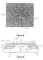
- the metallic layer 4 may be appropriately lithographically patterned for electroforming walls that define ink channels 36 and ink chambers 38 on an orifice plate as shown in Figure 4.
- Figure 5 shows a mandrel according to another embodiment for making orifice plates of non-uniform thicknesses. Instead of etching a gap 20, a step 40 is introduced on a substrate 6 to electrically isolate mandrel regions for forming the border 32 and orifice area 34. This step 40 can be etched in a polished silicon wafer substrate or created on a glass substrate by adding a layer of thick photoresist.
- Figure 5 also shows a non-uniformly thick orifice plate 42 electroformed on such a mandrel.
- the orifice plate 42 that is formed has a substantially flat surface 44 that allows easier attachment to a barrier layer (not shown) of a printhead die.
- FIG. 6 is an enlarged cross-sectional view of a mandrel according to yet another embodiment of the present invention.
- This mandrel has a metallic layer 4 preferably of only chrome.
- This chromium layer 4 has a first molding surface 18 electrically isolated from a second molding surface 19 just like those discussed above. In this mandrel, the dielectric layer is not included. Orifices are electroformed in holes etched through the second molding surface 19.
- Figures 7A- 7E show the various stages of making the mandrel in Figure 6. These stages are similar to those shown in Figures 2A-2E. The only difference is in the pattern 11 on the photomask 12.
- the pattern 11 used here further defines unmasked circles 50 on the metallic layer 4.
- the metallic layer 4 under these unmasked circles are etched away to define the holes in the seconding molding surface 19.
Landscapes
- Engineering & Computer Science (AREA)
- Manufacturing & Machinery (AREA)
- Chemical & Material Sciences (AREA)
- Chemical Kinetics & Catalysis (AREA)
- Electrochemistry (AREA)
- Materials Engineering (AREA)
- Metallurgy (AREA)
- Organic Chemistry (AREA)
- Particle Formation And Scattering Control In Inkjet Printers (AREA)
Abstract
Description
- This invention relates to a mandrel, a method of making the mandrel and orifice plates electroformed using the mandrel. The orifice plate that is formed has a thin orifice area surrounded by a thicker border. The thinner orifice area allows more orifices to be packed into a given area while the thicker border allows the orifice plate to withstand the rigors of manufacturing.
- A prior-art mandrel for electroforming orifice plates has a substrate of glass, plastic or a polished silicon wafer. A thin film layer of conductive material is deposited on this substrate. The conductive material is typically of chrome and stainless steel. A layer of dielectric is deposited on the conductive layer. This dielectric layer is of a nonconductive material such as silicon carbide. Patterns on the dielectric layer are lithographically formed using conventional masking, ultraviolet exposure and etching techniques to dimensionally define a molding surface for molding orifices in orifice plates. U.S. Patent 4,773,971 discloses a method of making such a mandrel.
- Orifice plates are formed on a mandrel in an electroforming process. The orifice plates thus formed are all on a single sheet. Breaking tabs that are also electroformed on the sheet defines the boundaries of each orifice plate. In the manufacturing of printheads, the sheet of orifice plates is attached to a mounting tape, for example, the Nitto Denko Elep Holder type V-8T available from Nitto Denko Corporation, Tokyo, Japan. The orifice plates are next singulated into individual orifice plates by breaking the sheet along the breaking tabs. The mounting tape holds the singulated orifice plates for further processing. A machine next picks and places each orifice plate over a corresponding printhead die on a wafer containing many such dies. The wafer and attached orifice plates are put through a "stake and bake" process to cause the orifice plates to adhere to the dies. After the "stake and bake" process, each printhead consisting of a die and an orifice plate is singulated using dice sawing. Each complete pair of orifice plate and printhead die is then ready for attaching to a pen body to complete the fabrication of an ink-jet pen. This pen body typically contains an ink reservoir which supplies ink to the printhead. In such a manufacturing process, the orifice plates are subjected to considerably rough handling during the steps of singulation and attachment to the printhead dies.
- To withstand such rigors in the manufacturing process, the orifice plates will have to be of a certain minimum thickness. As the size of an orifice is directly proportional to the thickness of an orifice plate due to the electroforming process, the thicker the orifice plate, the larger will be the orifices. These larger orifices will mean that fewer orifices can be packed into a given area, thus limiting the orifice count and resolution of an orifice plate. It is therefore desirable to keep the orifice plate thin so as to allow more orifices to be packed into a given area, since the orifices will be relatively smaller. However, this desirability contradicts the requirement to keep the orifice plates sufficiently thick for reasons previously discussed.
- Prior art mandrels can only form orifice plates that are substantially uniformly thick. There is therefore the need for a new mandrel and method for electroforming orifice plates of a non-uniform thickness.
- In one aspect of the present invention, a mandrel according to one embodiment has a metallic layer on a substrate. The metallic layer has a first molding surface that is electrically isolated from a second molding surface. The second molding surface is for substantially electroforming an orifice area of an orifice plate. The first molding surface is for substantially electroforming portions on the orifice plate that are thicker than the orifice area. These thicker portions are preferably portions that form a border around the orifice area. The mandrel also has means for electroforming orifices in the orifice area. In use, the first molding surface is predominantly allowed to electroform the thicker portions without the second molding surface electroforming the orifice area. As the thicker portions build up, they electrically connect the first and the second molding surfaces to allow the second molding surface to subsequently electroform the orifice area. The orifice plate thus formed is non-uniformly thick.
- In another aspect of the present invention, a preferred method of making the above mandrel involves depositing a metallic layer on a substrate followed by depositing a first photoresist layer on the metallic layer. Next, a first photomask having a first pattern is positioned on the first photoresist layer. The first photomask and the first photoresist layer are exposed to ultraviolet light for a predetermined period. After the exposure, the first photoresist layer is developed to produce the first pattern on the metallic layer. The portions of the metallic layer exposed by the first pattern of the first photomask is then etched to define the first and second molding surfaces. The method also includes introducing means for electroforming orifices in the orifice area. The remaining photoresist layer is stripped from the etched metallic layer. Preferably, introducing means for electroforming orifices in the orifice area involves stripping the remaining first photoresist layer and depositing a dielectric layer on the etched metallic layer followed by depositing a second photoresist layer on the dielectric layer. A second photomask having a second pattern is positioned on the second photoresist layer. Similarly, the second photomask and the second photoresist layer are exposed to ultraviolet light. Again, after exposure, the second photoresist layer is developed to produce the second pattern on the dielectric layer. The portions of the dielectric layer that are exposed by the second pattern are etched to define the dielectric areas.
- In yet another aspect, an orifice plate electroformed using the above mandrel has an orifice area and portions that are thicker than the orifice area. The orifice area has orifices electroformed on it. The thicker portions are preferably portions of the orifice plate that form a border surrounding the orifice area. The border preferably completely surrounds the orifice area.
- The invention will be better understood with reference to the drawings, in which:
- Figure 1A is a cross-sectional view of a mandrel taken along a line X-X in Figure 1B.
- Figure 1B is a plan view of the mandrel in Figure 1A.
- Figures 2A-2H are isometric views of the mandrel in Figure 1A in different stages of a process for making the mandrel.
- Figures 3A-3D are cross-sectional views similar to that in Figure 1A showing stages of electroforming an orifice plate using the mandrel.
- Figure 4 is an isometric view of a portion of an orifice plate electroformed using a mandrel according to an alternative embodiment.
- Figure 5 is a cross-sectional view of a mandrel according to yet another embodiment of the present invention.
- Figure 6 is a cross-sectional view of a mandrel according to an embodiment that does not require a dielectric layer.
- Figures 7A-7E are isometric views of the mandrel in Figure 6 in different stages of a process for making the mandrel.
-
- Figures 1A and 1B show an illustrative
reusable mandrel 2 for electroforming an orifice plate. Thismandrel 2 is shown to be able to form only one orifice plate. It is well known to those skilled in the art that given the size of an orifice plate and the surface area of a substrate of themandrel 2, many orifice plates can be formed simultaneously using a single mandrel. Figure 1A is an enlarged cross-sectional view of themandrel 2. Themandrel 2 has a conductivethin film 4 deposited on asubstrate 6. Examples of substrates are a glass substrate, a plastic substrate or a polished silicon wafer. This conductivethin film 4 preferably ranges from 100 angstroms to 200 microns thick. Other thickness ranges are possible. This conductivethin film 4 is preferably made up of a layer of chrome 4-1 beneath a layer of stainless steel 4-2. The chrome layer 4-1 bonds firmly to thesubstrate 6 and provides a surface that the stainless steel layer 4-2 can adhere to. Adielectric layer 8 is deposited on top of the conductivethin film 4. Thisdielectric layer 8 is shown having been patterned and etched to form a molding surface for electroforming orifices in an orifice plate. - Figures 2A-2H show the different stages of a process for making the
mandrel 2. This process is similar to that disclosed in U.S. Patent 4,773,971. However, the image or pattern on a photomask used in the making of the mandrel changes the structure of the completed mandrel substantially to render it significantly advantageous over the prior art mandrel disclosed in the patent. - The process starts with using a vacuum deposition process, such as the planar magnetron process to deposit a metallic layer or conductive
thin film 4 on asubstrate 6 of any smooth and non-conducting surface. This conductivethin film 4 is preferably of chrome and stainless steel. Figure 2A shows the conductivethin film 4 on thesubstrate 6. - Next, a spinning process is used to deposit a
photoresist layer 10 on top of the conductivethin film 4 as shown in Figure 2B. Thisphotoresist layer 10 is either positive or negative depending on the image orpattern 11 on a photomask 12 (Figure 2C). Thephotomask 12 is next placed on thephotoresist layer 10. The combination of thephotomask 12 andphotoresist layer 10 is then exposed to ultra-violet (UV) light as shown in Figure 2C. After exposure to UV light, thephotomask 12 is removed and thephotoresist layer 10 is developed so that it bears thepattern 11. Thepattern 11 definesmasked regions 14 and unmaskedregions 16 of the conductivethin film 4 as shown in Figure 2D. Next, an etching process such as sputter-etching or chemical etching is used to completely etch the unmaskedthin film regions 16. Figure 2E shows the resultant conductivethin film 4 after etching. The etching defines afirst molding surface 18, asecond molding surface 19 and agap 20 therebetween. The first and second molding surfaces 18, 19 are for forming thicker portions and an orifice area of an orifice plate respectively. For example, the thicker portions can be portions on the orifice plate forming a border around the orifice area. For such configuration, thefirst molding surface 18 preferably completely surrounds thesecond molding surface 19. The twomolding surfaces thin film 4 link the first molding surfaces 18 so that they are all electrically connected. - Next, a plasma enhanced chemical vapor deposition process is used to deposit a
dielectric layer 8 of silicon nitride on the etched conductivethin film 4 andsubstrate 6, as shown in Figure 2F. The molding surfaces 18, 19 are not visible in Figure 2F as thedielectric layer 8 covers them. Other nonconductive materials can also be used for thislayer 8. Next, asecond photoresist layer 22 is applied on thedielectric layer 8. Again, depending on the photomask image, either positive or negative photoresist is used. After thephotoresist layer 22 is applied, asecond photomask 24 havingbutton patterns 26 is placed over thephotoresist layer 22. The combination of thesecond photomask 24 and thephotoresist layer 22 is exposed to UV light as shown in Figure 2G. After an appropriate period of exposure, thephotomask 24 is removed and the photoresist layer is developed to leave masked and unmasked regions (not shown) on thedielectric layer 8 beneath it. An etching process, such as plasma etching, is used to remove the unmasked regions of thedielectric layer 8. After the etching process the remaining photoresist layer is removed to leavedielectric buttons 8 on the conductivethin film 4 as shown in Figure 2H. Thesedielectric buttons 8 form molding surfaces for electroforming orifices in the orifice area of an orifice plate. Thesedielectric buttons 8 can be arranged in any suitable manner but is commonly arranged in two rows. When arranged in this manner, the first molding surface may include a surface (not shown) that runs between the two rows of the dielectric buttons. The mandrel is then ready for use in electroforming an orifice plate. - When used to electroform an orifice plate, the
mandrel 2 is inserted into an electroforming bath as a cathode. Ametal source material 28 which supplies the electroforming material is made an anode. The source material plate is preferably composed of a non-ink-corrosive metal such as a nickel alloy. During the electroforming process, current is initially allowed to flow through the conductive thin film regions that define the first molding surfaces 18 of the mandrel. Since the conductive thin film regions defining the second molding surfaces 19 are electrically isolated from the firstmolding surface regions 18, little or no current passes through the secondmolding surface regions 19 of the conductivethin film 4. Themetal 28 is transferred from the anode metal plate onto the first molding surfaces 18 as shown in Figure 3A. Since the electroforming bath is also a conductor, there will be leakage currents flowing through the secondmolding surface regions 19 of the conductivethin film 4. Such leakage currents will also cause metal to be deposited on thesecond molding surface 19. However, the buildup of metal on this surface 19 (not shown in Figure 3A) is substantially slower than that on thefirst molding surface 18. - Over time the buildup of
metal 28 around thefirst molding surface 18 bridges thegap 20 between the twomolding surfaces molding surfaces metal 28 will also start to substantially collect on thesecond molding surface 19 in addition to collecting on thefirst molding surface 18. Such deposition of metal is shown in Figure 3C. As substantial deposition of metal occurs later on thesecond molding surface 19, less metal is deposited on thissurface 19. As the electroforming process continues, metal will be deposited around thedielectric buttons 8 to form theorifices 30. The electroforming process is continued until a desired thickness of metal is deposited on the molding surfaces 18,19 anddielectric buttons 8. The electroforming of the orifice plate is then completed as shown in Figure 3D. - The orifice plate is stripped from the
mandrel 2 and preferably gold plated before it is ready for attachment to a printhead die. The orifice plate has athicker border 32 and athinner orifice area 34. With the ability to control the delay in electroforming theorifice area 34, the thickness of theorifice area 34 can be controlled with respect to the thickness of theborder 32. With proper selection of the width of thegap 20, orifice plates that haveborders 32 that are strong enough to withstand the rigors of manufacturing andorifice areas 34 that allow more orifices to be packed into a given area can be obtained. The general steps in the electroforming process just discussed are well known to those skilled in the art. The profile of accumulation of metal on themandrel 2 is also well known. - There is a relationship between the width of the
gap 20 and the relative thicknesses of theborder 32 andorifice area 34. The wider thegap 20, the larger will be the difference in thicknesses of theborder 32 and theorifice area 34. The table below shows some of the results obtained with different widths of thegap 20.Gap Width (Microns) Thickness of Border and Orifice Area (Microns) Plating Time, T1 Plating Time, T2 (<T1) 0 51.07 29.35 20 46.84 21.45 30 41.25 16.66 40 38.10 11.90 - The row with gap width equals zero (1st row of table) indicates that there is no
gap 20 between the molding surfaces 18, 19. Electroforming an orifice plate using such a mandrel will result in a substantially uniformly thick orifice plate of thicknesses of 51.07 and 29.35 microns for electroplating times of T1 and T2 respectively. There is no distinction between the border and orifice area of an orifice plate thus formed. - For a mandrel with a gap width of 30 microns (3rd row of table) used in an electroforming process for a time T1, the
border 32 of an electroformed orifice plate will have a thickness of 51.07 microns and theorifice area 34 will have a thickness of 41.25 microns. From the results obtained, it can be seen that as the gap is widened, the difference in thicknesses of theborder 32 and theorifice area 34 increases. A border thickness in a range of 30 to 50 microns is suitable for withstanding the rigors of manufacturing. The thickness of theorifice area 34 is preferably in a range of 10-20 microns. Other ranges of thicknesses are possible for theborder 32 and theorifice area 34. - The invention should not be construed to be limited to the embodiment discussed above. A person skilled in the art would readily know that other configurations of the orifice plates could be electroformed using a mandrel with electrically isolated molding surfaces. For example, the
metallic layer 4 may be appropriately lithographically patterned for electroforming walls that defineink channels 36 andink chambers 38 on an orifice plate as shown in Figure 4. - Such a person would also know that other processes could be used to produce different configurations of the mandrel. Figure 5 shows a mandrel according to another embodiment for making orifice plates of non-uniform thicknesses. Instead of etching a
gap 20, astep 40 is introduced on asubstrate 6 to electrically isolate mandrel regions for forming theborder 32 andorifice area 34. Thisstep 40 can be etched in a polished silicon wafer substrate or created on a glass substrate by adding a layer of thick photoresist. Figure 5 also shows a non-uniformlythick orifice plate 42 electroformed on such a mandrel. Theorifice plate 42 that is formed has a substantiallyflat surface 44 that allows easier attachment to a barrier layer (not shown) of a printhead die. - Figure 6 is an enlarged cross-sectional view of a mandrel according to yet another embodiment of the present invention. This mandrel has a
metallic layer 4 preferably of only chrome. Thischromium layer 4 has afirst molding surface 18 electrically isolated from asecond molding surface 19 just like those discussed above. In this mandrel, the dielectric layer is not included. Orifices are electroformed in holes etched through thesecond molding surface 19. - Figures 7A- 7E show the various stages of making the mandrel in Figure 6. These stages are similar to those shown in Figures 2A-2E. The only difference is in the
pattern 11 on thephotomask 12. Thepattern 11 used here further defines unmaskedcircles 50 on themetallic layer 4. Themetallic layer 4 under these unmasked circles are etched away to define the holes in the secondingmolding surface 19. - With the ability to electroform non-uniformly thick orifice plates, it is also possible to electroform orifice plates for a pen containing multi-colored inks. By adjusting the gaps between molding surfaces of an appropriate mandrel, different sections of the orifice plate can be electroformed to give different sizes and therefore resolutions of orifices.
Claims (16)
- A mandrel for electroforming orifice plates, each orifice plate having an orifice area containing orifices and portions of the orifice plate that is substantially thicker than the orifice area, the mandrel comprising:whereby electroforming an orifice plate on the mandrel involves first electroforming the thicker portions of the orifice plate on the first molding surface and allowing the electroformed thicker portions to electrically connect the first and second molding surfaces to subsequently electroform the orifice area.a substrate;a metallic layer on the substrate having a first molding surface for substantially electroforming the thicker portions and a second molding surface for substantially electroforming the orifice area, wherein the first and second molding surfaces are electrically isolated; andmeans on the metallic layer for electroforming orifices in the orifice area;
- A mandrel according to claim 1, wherein the means for electroforming orifices in the orifice area are dielectric areas patterned on the metallic layer.
- A mandrel according to claim 1, wherein the means for electroforming orifices in the orifice area are holes in the metallic layer.
- A mandrel according to claim 1, wherein the first molding surface is patterned for further electroforming regions on an orifice plate for defining ink chambers and ink channels.
- A mandrel according to claim 1, wherein a step is created on the substrate to separate the first and second molding surfaces of the metallic layer.
- A method of making a mandrel for electroforming orifice plates, each orifice plate having an orifice area containing orifices and portions of the orifice plate that is substantially thicker than the orifice area, the method comprising:depositing a metallic layer on a substrate;depositing a first photoresist layer on the metallic layer;positioning a first photomask having a first pattern on the first photoresist layer;exposing the first photomask and the first photoresist layer to ultraviolet light;developing the first photoresist layer to produce the first pattern on the metallic layer;etching portions of the metallic layer exposed by the first pattern of the first photomask to define a first molding surface for substantially electroforming the thicker portions and a second molding surface for substantially electroforming the orifice area, wherein the first and the second molding surfaces are electrically isolated;introducing means for electroforming orifices in the orifice area; andstripping substantially any remaining photoresist layer to complete the making of the mandrel.
- A method according to claim 6, wherein introducing means for electroforming orifices in the orifice are includes etching of the metallic layer to define holes in the orifice area.
- A method according to claim 6, wherein introducing means for electroforming orifices in the orifice area includes:stripping substantially any remaining photoresist layer;depositing a dielectric layer on the etched metallic layer;positioning a second photomask having a second pattern on the second photoresist layer;exposing the second photomask and the second photoresist layer to ultraviolet light;developing the second photoresist layer exposed by the second pattern of the second photomask to define dielectric areas for electroforming orifices in the orifice area.
- A method of making a mandrel according to claim 6, further comprising introducing a step on the substrate for electrically isolating the first and the second molding surfaces of the metallic layer.
- A method of making a mandrel according to claim 9, wherein the substrate is a polished silicon wafer and wherein introducing a step on the substrate involves photolithographically producing a pattern on the polished silicon wafer and etching the polished silicon wafer to produce the step.
- A method of making a mandrel according to claim 9, wherein introducing a step on the substrate involves:depositing a thick photoresist layer on the substrate;photolithographically producing a pattern on the thick photoresist layer; andetching the thick photoresist layer to produce the thick photoresist layer; andetching the thick photoresist layer to produce the step on the substrate.
- A method as in claim 6 for electroforming orifice plates, further comprising:allowing the electroformed thicker portions to build up to electrically connect the second molding surface so as to allow the second molding surface to commence substantially electroforming the orifice area of the orifice plate;substantially electroforming only the thicker portions of an orifice plate on the first molding surface;continuing to electroform both the thicker portions and the orifice area to predetermined thicknesses to produce a completed orifice plate; andremoving the completed orifice plate from the mandrel
- An orifice plate comprising:an orifice area having orifices therethrough; andportions on the orifice plate which are substantially thicker than the orifice area for rendering the orifice plate sufficiently strong to withstand manufacturing rigors.
- An orifice plate according to claim 13, wherein the thicker portions on the orifice plate are portions that form a border surrounding the orifice area.
- An orifice plate according to claim 14, wherein the orifices are arranged in two rows in the orifice area and the orifice plate further includes a thicker portion in the orifice area between the two rows of orifices.
- An orifice plate according to claim 13, wherein the thickness of the thicker portions is in a range of 30-50 microns and the orifice area is of a thickness in a range of 10-20 microns.
Applications Claiming Priority (2)
| Application Number | Priority Date | Filing Date | Title |
|---|---|---|---|
| US09/629,402 US6586112B1 (en) | 2000-08-01 | 2000-08-01 | Mandrel and orifice plates electroformed using the same |
| US629402 | 2000-08-01 |
Publications (2)
| Publication Number | Publication Date |
|---|---|
| EP1179614A2 true EP1179614A2 (en) | 2002-02-13 |
| EP1179614A3 EP1179614A3 (en) | 2003-01-02 |
Family
ID=24522854
Family Applications (1)
| Application Number | Title | Priority Date | Filing Date |
|---|---|---|---|
| EP01306613A Withdrawn EP1179614A3 (en) | 2000-08-01 | 2001-08-01 | Mandrel for electroforming orifice plates |
Country Status (5)
| Country | Link |
|---|---|
| US (1) | US6586112B1 (en) |
| EP (1) | EP1179614A3 (en) |
| JP (1) | JP3851789B2 (en) |
| CN (1) | CN1265027C (en) |
| TW (1) | TW593777B (en) |
Cited By (4)
| Publication number | Priority date | Publication date | Assignee | Title |
|---|---|---|---|---|
| WO2003095707A3 (en) * | 2002-05-07 | 2005-08-18 | Memgen Corp | Method of and apparatus for forming three-dimensional structures |
| GB2419357A (en) * | 2004-10-20 | 2006-04-26 | Dek Int Gmbh | Mandrels for electroforming printing screens and methods of forming screens thereby. |
| EP1950040A3 (en) * | 2001-09-12 | 2008-08-20 | Canon Kabushiki Kaisha | Liquid discharge recording head and method for manufacturing the same |
| CN102602151A (en) * | 2011-01-21 | 2012-07-25 | 施乐公司 | Polymer layer removal on pzt arrays using a plasma etch |
Families Citing this family (10)
| Publication number | Priority date | Publication date | Assignee | Title |
|---|---|---|---|---|
| US6790325B2 (en) * | 2001-04-09 | 2004-09-14 | Hewlett-Packard Development Company, L.P. | Re-usable mandrel for fabrication of ink-jet orifice plates |
| CN1324409C (en) * | 2002-03-15 | 2007-07-04 | 精工爱普生株式会社 | Method for preparing toner and toner and printed matter |
| JP4840756B2 (en) | 2005-01-14 | 2011-12-21 | セイコーインスツル株式会社 | Electroforming mold, manufacturing method thereof, and manufacturing method of electroformed part |
| US7501228B2 (en) * | 2005-03-10 | 2009-03-10 | Eastman Kodak Company | Annular nozzle structure for high density inkjet printheads |
| EP2053146B1 (en) | 2006-08-07 | 2016-08-31 | Seiko Instruments Inc. | Method for manufacturing electroformed mold, electroformed mold, and method for manufacturing electroformed parts |
| JP4963580B2 (en) * | 2006-09-04 | 2012-06-27 | 富士フイルム株式会社 | Nozzle plate manufacturing method, droplet discharge head manufacturing method, and image forming apparatus |
| EP2658719B1 (en) * | 2010-12-28 | 2018-08-29 | Stamford Devices Limited | Photodefined aperture plate and method for producing the same |
| EP3476982A1 (en) | 2012-06-11 | 2019-05-01 | Stamford Devices Limited | A method of producing an aperture plate for a nebulizer |
| WO2015177311A1 (en) | 2014-05-23 | 2015-11-26 | Stamford Devices Limited | A method for producing an aperture plate |
| KR102444290B1 (en) * | 2017-07-18 | 2022-09-16 | 삼성전자주식회사 | Method of bonding interposer and integrated chip, and ultrasonic probe using the method |
Citations (1)
| Publication number | Priority date | Publication date | Assignee | Title |
|---|---|---|---|---|
| US6511156B1 (en) * | 1997-09-22 | 2003-01-28 | Citizen Watch Co., Ltd. | Ink-jet head nozzle plate, its manufacturing method and ink-jet head |
Family Cites Families (19)
| Publication number | Priority date | Publication date | Assignee | Title |
|---|---|---|---|---|
| US4107699A (en) * | 1977-08-15 | 1978-08-15 | The Mead Corporation | Trenched stimulating plate |
| US4229265A (en) * | 1979-08-09 | 1980-10-21 | The Mead Corporation | Method for fabricating and the solid metal orifice plate for a jet drop recorder produced thereby |
| US4430784A (en) | 1980-02-22 | 1984-02-14 | Celanese Corporation | Manufacturing process for orifice nozzle devices for ink jet printing apparati |
| US4374707A (en) * | 1981-03-19 | 1983-02-22 | Xerox Corporation | Orifice plate for ink jet printing machines |
| US4678680A (en) * | 1986-02-20 | 1987-07-07 | Xerox Corporation | Corrosion resistant aperture plate for ink jet printers |
| US4773971A (en) | 1986-10-30 | 1988-09-27 | Hewlett-Packard Company | Thin film mandrel |
| NL8603278A (en) * | 1986-12-23 | 1988-07-18 | Stork Veco Bv | MEMBRANE WITH PERFORATIONS AND METHOD FOR MANUFACTURING SUCH MEMBRANE. |
| US4839001A (en) * | 1988-03-16 | 1989-06-13 | Dynamics Research Corporation | Orifice plate and method of fabrication |
| US4827287A (en) * | 1988-08-08 | 1989-05-02 | Eastman Kodak Company | Continuous ink jet printer having improved stimulation waveguide construction |
| GB8824283D0 (en) | 1988-10-17 | 1988-11-23 | Elmjet Ltd | Method for forming ink jet printer nozzle arrays |
| US4972204A (en) * | 1989-08-21 | 1990-11-20 | Eastman Kodak Company | Laminate, electroformed ink jet orifice plate construction |
| US4971665A (en) * | 1989-12-18 | 1990-11-20 | Eastman Kodak Company | Method of fabricating orifice plates with reusable mandrel |
| US5149419A (en) * | 1991-07-18 | 1992-09-22 | Eastman Kodak Company | Method for fabricating long array orifice plates |
| US5560837A (en) * | 1994-11-08 | 1996-10-01 | Hewlett-Packard Company | Method of making ink-jet component |
| NL1002908C2 (en) | 1996-04-19 | 1997-10-21 | Stork Veco Bv | Electroforming die, method of manufacture thereof, electroforming method and electroformed product. |
| NL1007317C2 (en) | 1997-10-20 | 1999-04-21 | Stork Veco Bv | A method of manufacturing a screen product, as well as a skeleton for use in the method, and a product thus obtained. |
| JP2001334671A (en) | 2000-05-26 | 2001-12-04 | Ricoh Co Ltd | Manufacturing method of inkjet nozzle |
| JP4370697B2 (en) | 2000-06-23 | 2009-11-25 | 株式会社村田製作所 | Screen printing plate and manufacturing method thereof |
| US6315385B1 (en) * | 2000-08-01 | 2001-11-13 | Hewlett-Packard Company | Self-locating orifice plate construction for thermal ink jet printheads |
-
2000
- 2000-08-01 US US09/629,402 patent/US6586112B1/en not_active Expired - Fee Related
-
2001
- 2001-02-26 TW TW090104385A patent/TW593777B/en not_active IP Right Cessation
- 2001-03-20 CN CN01111753.2A patent/CN1265027C/en not_active Expired - Fee Related
- 2001-07-31 JP JP2001231402A patent/JP3851789B2/en not_active Expired - Fee Related
- 2001-08-01 EP EP01306613A patent/EP1179614A3/en not_active Withdrawn
Patent Citations (1)
| Publication number | Priority date | Publication date | Assignee | Title |
|---|---|---|---|---|
| US6511156B1 (en) * | 1997-09-22 | 2003-01-28 | Citizen Watch Co., Ltd. | Ink-jet head nozzle plate, its manufacturing method and ink-jet head |
Non-Patent Citations (1)
| Title |
|---|
| Retrieved from the Internet <URL:http://www.m-w.com/dictionary/flat> [retrieved on 20080124] * |
Cited By (6)
| Publication number | Priority date | Publication date | Assignee | Title |
|---|---|---|---|---|
| EP1950040A3 (en) * | 2001-09-12 | 2008-08-20 | Canon Kabushiki Kaisha | Liquid discharge recording head and method for manufacturing the same |
| WO2003095707A3 (en) * | 2002-05-07 | 2005-08-18 | Memgen Corp | Method of and apparatus for forming three-dimensional structures |
| GB2419357A (en) * | 2004-10-20 | 2006-04-26 | Dek Int Gmbh | Mandrels for electroforming printing screens and methods of forming screens thereby. |
| GB2419357B (en) * | 2004-10-20 | 2010-04-21 | Dek Int Gmbh | Mandrels for electroforming printing screens, electroforming systems for electroforming printing screens, methods of electroforming printing screens. |
| CN102602151A (en) * | 2011-01-21 | 2012-07-25 | 施乐公司 | Polymer layer removal on pzt arrays using a plasma etch |
| CN102602151B (en) * | 2011-01-21 | 2015-09-23 | 施乐公司 | Form the method for ink jet printing head |
Also Published As
| Publication number | Publication date |
|---|---|
| JP2002115089A (en) | 2002-04-19 |
| CN1336450A (en) | 2002-02-20 |
| CN1265027C (en) | 2006-07-19 |
| JP3851789B2 (en) | 2006-11-29 |
| TW593777B (en) | 2004-06-21 |
| EP1179614A3 (en) | 2003-01-02 |
| US6586112B1 (en) | 2003-07-01 |
Similar Documents
| Publication | Publication Date | Title |
|---|---|---|
| EP0273552B1 (en) | Method of making mandrels for use in a deposition process | |
| US6586112B1 (en) | Mandrel and orifice plates electroformed using the same | |
| US5560837A (en) | Method of making ink-jet component | |
| EP0485182B1 (en) | Thermal inkjet thin film printhead having a plastic orifice plate and method of manufacture | |
| EP0112701B1 (en) | Valve element for use in an ink-jet printer head | |
| JP2716174B2 (en) | Inkjet print head | |
| US5131978A (en) | Low temperature, single side, multiple step etching process for fabrication of small and large structures | |
| US5443713A (en) | Thin-film structure method of fabrication | |
| TW201013329A (en) | Method of fabricating multi-level metallic parts by the LIGA-UV technique | |
| US5236572A (en) | Process for continuously electroforming parts such as inkjet orifice plates for inkjet printers | |
| US6497019B1 (en) | Manufacturing method of ink jet printer head | |
| EP1080907A2 (en) | Manufacturing printheads | |
| US6562642B1 (en) | Micro-structures and methods for their manufacture | |
| JPH05239682A (en) | Electroforming method | |
| EP0713929B1 (en) | Thin film pegless permanent orifice plate mandrel | |
| US6379871B1 (en) | Method for fabricating a mask for a LIGA process | |
| EP0520760A1 (en) | Method for producing orifice plate | |
| KR100228765B1 (en) | Cell Aperture Mask Manufacturing Method | |
| JPH08142333A (en) | Nozzle plate master mold and nozzle plate manufacturing method | |
| JP4164592B2 (en) | Stamper manufacturing method | |
| US11181868B2 (en) | Method for manufacturing a timepiece component and component obtained by this method | |
| JP2006001046A (en) | Manufacturing method of mold for fine pattern molding | |
| KR20010047178A (en) | Manufacturing method for stencil mask | |
| JPH08132625A (en) | Nozzle plate manufacturing method and master mold structure therefor | |
| JPH05286141A (en) | Orifice plate manufacturing method |
Legal Events
| Date | Code | Title | Description |
|---|---|---|---|
| PUAI | Public reference made under article 153(3) epc to a published international application that has entered the european phase |
Free format text: ORIGINAL CODE: 0009012 |
|
| AK | Designated contracting states |
Kind code of ref document: A2 Designated state(s): AT BE CH CY DE DK ES FI FR GB GR IE IT LI LU MC NL PT SE TR |
|
| AX | Request for extension of the european patent |
Free format text: AL;LT;LV;MK;RO;SI |
|
| PUAL | Search report despatched |
Free format text: ORIGINAL CODE: 0009013 |
|
| AK | Designated contracting states |
Kind code of ref document: A3 Designated state(s): AT BE CH CY DE DK ES FI FR GB GR IE IT LI LU MC NL PT SE TR |
|
| AX | Request for extension of the european patent |
Free format text: AL;LT;LV;MK;RO;SI |
|
| RIC1 | Information provided on ipc code assigned before grant |
Free format text: 7C 25D 1/10 A, 7C 25D 1/08 B, 7B 41J 2/16 B |
|
| 17P | Request for examination filed |
Effective date: 20030702 |
|
| AKX | Designation fees paid |
Designated state(s): DE FR GB |
|
| 17Q | First examination report despatched |
Effective date: 20080131 |
|
| RAP1 | Party data changed (applicant data changed or rights of an application transferred) |
Owner name: HEWLETT-PACKARD DEVELOPMENT COMPANY, L.P. |
|
| STAA | Information on the status of an ep patent application or granted ep patent |
Free format text: STATUS: THE APPLICATION IS DEEMED TO BE WITHDRAWN |
|
| 18D | Application deemed to be withdrawn |
Effective date: 20150303 |