EP1178699A2 - Transport interface for time division frames - Google Patents
Transport interface for time division frames Download PDFInfo
- Publication number
- EP1178699A2 EP1178699A2 EP01401962A EP01401962A EP1178699A2 EP 1178699 A2 EP1178699 A2 EP 1178699A2 EP 01401962 A EP01401962 A EP 01401962A EP 01401962 A EP01401962 A EP 01401962A EP 1178699 A2 EP1178699 A2 EP 1178699A2
- Authority
- EP
- European Patent Office
- Prior art keywords
- frames
- time division
- ear
- circuit means
- transport interface
- Prior art date
- Legal status (The legal status is an assumption and is not a legal conclusion. Google has not performed a legal analysis and makes no representation as to the accuracy of the status listed.)
- Granted
Links
Images

Classifications
-
- H—ELECTRICITY
- H04—ELECTRIC COMMUNICATION TECHNIQUE
- H04J—MULTIPLEX COMMUNICATION
- H04J3/00—Time-division multiplex systems
- H04J3/16—Time-division multiplex systems in which the time allocation to individual channels within a transmission cycle is variable, e.g. to accommodate varying complexity of signals, to vary number of channels transmitted
- H04J3/1605—Fixed allocated frame structures
- H04J3/1611—Synchronous digital hierarchy [SDH] or SONET
-
- H—ELECTRICITY
- H04—ELECTRIC COMMUNICATION TECHNIQUE
- H04Q—SELECTING
- H04Q11/00—Selecting arrangements for multiplex systems
- H04Q11/04—Selecting arrangements for multiplex systems for time-division multiplexing
- H04Q11/0428—Integrated services digital network, i.e. systems for transmission of different types of digitised signals, e.g. speech, data, telecentral, television signals
- H04Q11/0478—Provisions for broadband connections
-
- H—ELECTRICITY
- H04—ELECTRIC COMMUNICATION TECHNIQUE
- H04J—MULTIPLEX COMMUNICATION
- H04J2203/00—Aspects of optical multiplex systems other than those covered by H04J14/05 and H04J14/07
- H04J2203/0001—Provisions for broadband connections in integrated services digital network using frames of the Optical Transport Network [OTN] or using synchronous transfer mode [STM], e.g. SONET, SDH
- H04J2203/0003—Switching fabrics, e.g. transport network, control network
- H04J2203/0025—Peripheral units
-
- H—ELECTRICITY
- H04—ELECTRIC COMMUNICATION TECHNIQUE
- H04J—MULTIPLEX COMMUNICATION
- H04J2203/00—Aspects of optical multiplex systems other than those covered by H04J14/05 and H04J14/07
- H04J2203/0001—Provisions for broadband connections in integrated services digital network using frames of the Optical Transport Network [OTN] or using synchronous transfer mode [STM], e.g. SONET, SDH
- H04J2203/0073—Services, e.g. multimedia, GOS, QOS
- H04J2203/0082—Interaction of SDH with non-ATM protocols
- H04J2203/0083—Support of the IP protocol
Definitions
- the present invention relates to a transport interface for time division frames, in particular SDH frames, and related interfacing method of time division frames.
- the various information streams, or data, propagating on telecommunication networks are multiplexed in frames according to predetermined transport protocols, such as SDH (Synchronous Digital Hierarchy) transport protocol for time division frames.
- SDH Serial Digital Hierarchy
- This transport protocol is particularly suitable for conveying and distributing the numerous information streams among the various telecommunications network nodes.
- various logic circuits are arranged inside the telecommunications network nodes, such as SDH network, apt to process in different ways the time division frame received from the node. These operations are essentially related to dealing with the synchronism and with the extraction of the various data streams multiplexed inside the time division frame, as well as with the subsequent processing of the various information streams extracted from said time division frames.
- an ASIC Application Specific Integrated Circuit
- a dedicated circuit which performs SDH operations on the frame by extracting and inserting the information streams, also called tributaries, from the so called Virtual Containers, wherein they are multiplexed.
- This ASIC circuit can be followed by FPGA (Field Programmable Gate Arrays) circuits, i.e. circuits adaptable according to their utilization and located outside the ASIC circuit, which process the tributaries extracted from the frame, such as processing the streams that use ATM (Asynchronous Transfer Mode) protocol or IP (Internet Protocol) protocol, previously multiplexed inside the SDH frame. Due to their flexibility, FPGA circuits are frequently employed in conjunction with dedicated circuits.
- ATM Asynchronous Transfer Mode
- IP Internet Protocol
- Communications between ASIC circuits and related FPGA circuits are usually defined as 'intra-equipment' communications, namely communications occurring inside the telecommunications network node, whereas communications between the nodes are called line communications.
- the same interface protocols employed for the nodes receiver interfaces are also used for the above intra-equipment communications of tributaries, such as the so called Network Node Interfaces, i.e. network node interfaces for line communications to other nodes.
- the interfaces of the ASIC circuit are not flexible, since they have to operate on different protocols, i.e. ATM or IP, which are not structure compatible.
- an ASIC circuit can communicate with a certain number of FPGA devices performing certain termination functions, e.g. operating according to ATM protocol, but cannot communicate with FPGA devices using IP protocol, unless they have further transport interfaces expressly provided for handling IP protocol available. This reduces ASIC circuit flexibility.
- a further object of the present invention is to provide a transport interface for time division frames, in particular SDH frames, which is flexible and can be utilized by any circuits implementing various termination functions.
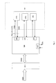
- Figure 1 is representing a basic diagram of the architecture of a telecommunications network, wherein the transport interface according to the present invention is operating.
- This figure shows a time division frames stream TRM structured according to the SDH protocol, said frames stream TRM being received by a network interface of the node NTI that transmits to the main board of a switch matrix SM, sending a frames streamTRM2 adapted for said switch matrix SM.
- This switch matrix SM is obtained through an ASIC circuit and extracts for instance the tributaries from the frames stream TRM and processes their addresses.
- the switch matrix SM communicates with a plurality of devices for processing the tributaries FP, external to the ASIC circuit and implemented by FPGA circuits, which perform the processing of the tributaries extracted from the switch matrix SM.
- FPA for processing the tributaries according to the ATM protocol
- FPI for processing the tributaries according to the Internet Protocol.
- the switch matrix SM is equipped with appropriate transport interfaces STI, which exchange a special data stream FDS with the devices for processing the tributaries FP.
- Said special data stream FDS comprises anyway a transmitted stream TXD, received by the device FP, and a received stream RXD, transmitted by the device FP and requested by the transport interface STI.
- a data stream FDS contains a data bus BD, sent in a co-directional mode in both directions, wherein the information contents of the tributary to be processed is conveyed, and a minimum set of signals, i.e. an auxiliary signal EAR accompanying the data bus BD, comprising enable information and identifying information of the payload, i.e. an address of the tributary or port wherefrom it is extracted.
- a minimum set of signals i.e. an auxiliary signal EAR accompanying the data bus BD, comprising enable information and identifying information of the payload, i.e. an address of the tributary or port wherefrom it is extracted.
- the device for processing the tributaries FP is only receiving data, information about the validity of said data through the enable information, and address information to allocate the tributary inside it.
- the transport interface STI will receive the data bus BD from the device for processing the tributaries FP sending the auxiliary signal EAR in the form of a request, i.e. the address information identifies the tributary requested by the transport interface STI, whereas the enable information will act as a request to send the payload.
- the transport interface STI of the switch matrix SM is shown, consisting of a receiver RXTI and transmitter TXTI.
- the transmitter TXTI receives at its input a plurality of Arbitrary Units AU0, AU1, AU2, AU3, which have been extracted inside the switch matrix SM from a frame TRM, and containing Tributary Unit tributaries, whose payload has to be sent in the transmitted stream TXD to the transport interface STI of the device for processing the tributaries FP.
- the pointers related to the AU and TU structures are taken out of the four Arbitrary Units AU0, AU1, AU2, AU3 through appropriate logic circuits PI, called Pointer Interpreters, and the Arbitrary Units are multiplexed at a quadruple frequency in a data bus T_BD by a suitable multiplexer BM also generating an auxiliary signal T_EAR.
- Figure 2 also shows a desynchronizing circuit DS, which according to known techniques drives the multiplexer BM to generate plesiochronous streams (no longer synchronous as inside the switch matrix SM).
- the receiver RXTI receives the transmitted data over a data bus R_BD and demultiplexes them at a lower frequency, through a demultiplexer DM, to a first insertion block BI controlled by a time base BT, which also controls the generation through a multiplexer MX of an auxiliary signal R_EAR, which requests the data to be mapped in the Virtual Containers of the frames TRM from the device for processing the tributaries FP.
- a synchronizing circuit SD is also provided, which controls, according to known mapping techniques, the flow of the data streams from the plesiochronous edge, represented by the data bus R_BD outside the transport interface STI, to the synchronous edge in the switch matrix SM.
- the synchronizing circuit SD supplies the timing to a multiplexer MX2, which receives the demultiplexed data streams from the insertion block BI and inserts them in the Arbitrary Units A0, A1, A2, A3, to be subsequently multiplexed.
- the signal in the data bus BD is an 8-bit signal either containing the payload of the tributary element extracted from the Virtual Container, in the case it belongs to the transmitted stream TXD, i.e. it is the data bus T_BD, or containing the payload to be inserted in a Virtual Container in the case it belongs to the received stream RXD, i.e. the data bus R_BD.
- the interface STI generates the auxiliary signal EAR, which corresponds to the above minimum set of signals required for the handling of the data bus BD by the device for processing the tributaries FP.
- the auxiliary signal T_EAR is actually a 9-bit signal: the bits 0 to 5 contain an address information of the tributaries being extracted, the bits 6 and 7 contain information about the Arbitrary Unit AU being extracted, the bit 8 is an enable bit, i.e. if it is at logic one, the data is valid for the receiver of the transport interface STI.
- the data bus T_DB and the auxiliary signal T_EAR form the transmitted stream TXD, which is received exactly from the device for processing the tributaries FP.
- the received stream RXD flowing from the processing device FP to the switch matrix SM, is substantially sent in reply to a data request signal issued by the transport interface STI, as mentioned above.
- a data request signal issued by the transport interface STI is the auxiliary signal R_EAR, wherein also the first 6 bits (0 to 5) contain information about the requested tributaries, bits 6 and 7 contain information about the requested Arbitrary Unit AU, whereas the bit 8 is a request enable bit.
- the tributaries processing device transmits the requested tributary to the data bus R_BD through the auxiliary signal R_EAR, to be mapped into an SDH Virtual Container by means of the switch matrix SM receiving it.
- the device for processing the tributaries FP supplies the data to be inserted, conveyed in the data bus BD, with a delay with respect to the auxiliary signal EAR.
- This delay can be set at a predetermined number of clock intervals, which can be reset, as per FPGA circuit requirements. In the event of a 77MHz operating frequency, this delay is 7 clock shots.
- the signals described in the above examples have a minimum configuration and are suitable for general protocols, such as Internet Protocol.
- a 1-bit synchronism signal utilized by the tributaries processing device FPA for marking the start of the ATM cells, as well as an alarm bit TSF for the device for processing tributaries FPA, can be sent into the transmitted stream TXD, besides the auxiliary signal T_EAR. In this event, additional pins for these signals can be provided.
- This synchronism signal can be alternatively used for marking a particular bit of the transport protocol or of the payload, such as in the case of Gbit Ethernet.
- the received stream RXD will equally contain in addition a synchronism bit, for the switch matrix SM, pointing to the correct bit of payload start, or a specific byte for the correct mapping in the ASIC.
- the transport interface for time division frames in particular SDH frames according to the present invention will advantageously make intra-equipment communication easier between the switch matrix or other central circuits for time division frames, and the peripheral frame processing devices. This will also simplify the control logic requested for processing information streams, i.e. reducing interface complexity.
- the transport interface for time division frames in particular SDH frames according to the present invention will advantageously increase ASIC circuit flexibility when in use with FPGA circuits; also in the case of the circuit having dedicated interfaces for special protocols, it can always be equipped with a transport interface covered by the present invention, so as to be able to take tributaries at any time according to a simple adaptable protocol and increase its flexibility.
- time division data frames on which the interface according to the present invention operates may have different formats.
Landscapes
- Engineering & Computer Science (AREA)
- Computer Networks & Wireless Communication (AREA)
- Signal Processing (AREA)
- Time-Division Multiplex Systems (AREA)
- Data Exchanges In Wide-Area Networks (AREA)
- Financial Or Insurance-Related Operations Such As Payment And Settlement (AREA)
- Stringed Musical Instruments (AREA)
- Electrical Discharge Machining, Electrochemical Machining, And Combined Machining (AREA)
- Diaphragms For Electromechanical Transducers (AREA)
Abstract
Description
- Fig. 1 shows a block diagram of a transport interface for time division frames, in particular SDH frames, according to the present invention;
- Fig. 2 shows a more detailed block diagram of the transport interface for time division frames, in particular SDH frames, of Figure 1.
In the instance of Figure 1, there are indicated by way of example two devices FPA for processing the tributaries according to the ATM protocol and a device FPI for processing the tributaries according to the Internet Protocol.
R_EAR(8:0)="1"&"00"& "00000"
Claims (11)
- Transport interface for time division frames, in particular SDH frames, being transmitted between network nodes according a specified transport protocol, said nodes comprising first circuit means (SM) for processing said time division frames (TRM, TRM2) according to said specified transport protocol, and second circuit means (FP) for exchanging second information streams (FDS) with said first circuit means (SM) through said transport interface (STI), characterized in that it provides for structuring said second information streams (FDS) as a data stream (BD, T_BD, R_BD), sent in a co-directional way, and an address information (EAR, T_EAR, R_EAR).
- Transport interface for time division frames, in particular SDH frames, according to claim 1, characterized in that the address information (EAR, T_EAR, R_EAR) comprises an enable information of the exchange of the second information streams (FDS).
- Transport interface for time division frames, in particular SDH frames, according to claim 2, characterized in that it sends the data stream (BD, T_BD, R_BD) and address information (EAR, T_EAR, R_EAR) with a reciprocal time delay.
- Transport interface for time division frames, in particular SDH frames, according to claim 3, characterized in that it comprises a transmitter (TXTI) for sending a data stream (T_BD) extracted from the time division frame (TRM2) and first address information (T_EAR).
- Transport interface for time division frames, in particular SDH frames, according to claim 3, characterized in that it comprises a receiver (RXTI) for receiving a data stream (R_BD) originated by the second circuit means (FP) and to send second address information (R_EAR) to said second circuit means (FP).
- Transport interface for time division frames, in particular SDH frames, according to claim 4, characterized in that said first address information (T_EAR) comprises an enable information and one or more address information of the transmitted data stream (T_BD).
- Transport interface for time division frames, in particular SDH frames, according to claim 5, characterized in that said second address information (R_EAR) comprises a transmission enable information for the second circuit means (FP) and one or more address information of the data stream (R_BD) requested from said second circuit means (FP).
- Transport interface for time division frames, in particular SDH frames, according to claim 6, characterized in that said first address information (T_EAR), in particular in the instance of ATM data stream (T_BD), comprises a synchronism signal, utilized by said second circuit means (FPA) for marking the start of ATM cells and/or an alarm bit TSF for the second circuit means (FP).
- Transport interface for time division frames, in particular SDH frames, according to claim 7, characterized in that said second address information (R_EAR), in particular in the instance of an ATM data stream (R_BD), comprises a synchronism signal for the first circuit means (SM), for marking the correct bit of payload start, for a correct handling in the first circuit means (SM) of the information transported by the payload.
- Transport interface for time division frames, in particular SDH frames, according to any of the previous claims, characterized in that the first circuit means (SM) are implemented by a dedicated ASIC circuit, whereas the second circuit means (FP) are implemented by FPGA circuits.
- Method for interfacing time division frames, in particular SDH frames, in a telecommunications network, which provides for extraction and exchange of the data streams multiplexed in said time division frames (TRM,TRM2) between a time division frame processing circuit (SM) and devices for processing (FP) the data streams contained in said time division frames (TRM,TRM2), characterized by comprising the step of allocating a data stream (BD, T_BD, R_BD) and an address information (EAR, T_EAR, R_EAR), for co-directional information exchange between the time division frame processing circuit (SM) and the processing devices (FP).
Applications Claiming Priority (2)
| Application Number | Priority Date | Filing Date | Title |
|---|---|---|---|
| IT2000TO000760A IT1320570B1 (en) | 2000-07-31 | 2000-07-31 | TRANSPORT INTERFACE FOR TIME-DIVIDING PLOTS. |
| ITTO000760 | 2000-07-31 |
Publications (3)
| Publication Number | Publication Date |
|---|---|
| EP1178699A2 true EP1178699A2 (en) | 2002-02-06 |
| EP1178699A3 EP1178699A3 (en) | 2004-12-15 |
| EP1178699B1 EP1178699B1 (en) | 2009-04-22 |
Family
ID=11457968
Family Applications (1)
| Application Number | Title | Priority Date | Filing Date |
|---|---|---|---|
| EP01401962A Expired - Lifetime EP1178699B1 (en) | 2000-07-31 | 2001-07-20 | Transport interface for time division frames |
Country Status (7)
| Country | Link |
|---|---|
| US (1) | US7023836B2 (en) |
| EP (1) | EP1178699B1 (en) |
| JP (1) | JP2002094503A (en) |
| AT (1) | ATE429741T1 (en) |
| CA (1) | CA2354327A1 (en) |
| DE (1) | DE60138439D1 (en) |
| IT (1) | IT1320570B1 (en) |
Cited By (2)
| Publication number | Priority date | Publication date | Assignee | Title |
|---|---|---|---|---|
| CN100336340C (en) * | 2003-06-24 | 2007-09-05 | 中兴通讯股份有限公司 | Multi-channel network management apparatus and method for transmission equipment |
| CN102223490A (en) * | 2011-06-22 | 2011-10-19 | 上海博康智能网络科技有限公司 | Digital switching matrix supporting synchronic switching and synchronic switching method of digital image |
Families Citing this family (5)
| Publication number | Priority date | Publication date | Assignee | Title |
|---|---|---|---|---|
| JP2002300130A (en) * | 2001-03-29 | 2002-10-11 | Nec Corp | System and device for overhead inserting/extracting for sonet/sdh |
| IL152626A0 (en) * | 2002-11-03 | 2003-06-24 | Hello Tech Technologies Ltd | Improved mobile payment system |
| KR100567211B1 (en) * | 2003-12-11 | 2006-04-03 | 한국전자통신연구원 | Random transmission data transmission system and method for orthogonal frequency division multiple access |
| GB2444745B (en) * | 2006-12-13 | 2011-08-24 | Advanced Risc Mach Ltd | Data transfer between a master and slave |
| CN101639792B (en) | 2008-07-29 | 2016-04-06 | 阿里巴巴集团控股有限公司 | A kind of concurrent data disposal route, device and a kind of electronic accounting system |
Family Cites Families (4)
| Publication number | Priority date | Publication date | Assignee | Title |
|---|---|---|---|---|
| US5583855A (en) * | 1993-11-10 | 1996-12-10 | Fujitsu Limited | Add/drop multiplexer apparatus |
| KR0150367B1 (en) * | 1995-12-19 | 1998-11-02 | 양승택 | Full combining type atm switching apparatus |
| US6778529B1 (en) * | 1999-12-01 | 2004-08-17 | Cisco Technology, Inc. | Synchronous switch and method for a telecommunications node |
| US6414966B1 (en) * | 2000-06-15 | 2002-07-02 | Oss Corporation | Bridging device for mapping/demapping ethernet packet data directly onto and from a sonet network |
-
2000
- 2000-07-31 IT IT2000TO000760A patent/IT1320570B1/en active
-
2001
- 2001-07-20 EP EP01401962A patent/EP1178699B1/en not_active Expired - Lifetime
- 2001-07-20 AT AT01401962T patent/ATE429741T1/en not_active IP Right Cessation
- 2001-07-20 DE DE60138439T patent/DE60138439D1/en not_active Expired - Lifetime
- 2001-07-24 US US09/910,811 patent/US7023836B2/en not_active Expired - Fee Related
- 2001-07-26 JP JP2001225571A patent/JP2002094503A/en not_active Withdrawn
- 2001-07-30 CA CA002354327A patent/CA2354327A1/en not_active Abandoned
Cited By (3)
| Publication number | Priority date | Publication date | Assignee | Title |
|---|---|---|---|---|
| CN100336340C (en) * | 2003-06-24 | 2007-09-05 | 中兴通讯股份有限公司 | Multi-channel network management apparatus and method for transmission equipment |
| CN102223490A (en) * | 2011-06-22 | 2011-10-19 | 上海博康智能网络科技有限公司 | Digital switching matrix supporting synchronic switching and synchronic switching method of digital image |
| CN102223490B (en) * | 2011-06-22 | 2013-04-10 | 博康智能网络科技股份有限公司 | Digital switching matrix supporting synchronic switching and synchronic switching method of digital image |
Also Published As
| Publication number | Publication date |
|---|---|
| ITTO20000760A1 (en) | 2002-01-31 |
| IT1320570B1 (en) | 2003-12-10 |
| EP1178699A3 (en) | 2004-12-15 |
| EP1178699B1 (en) | 2009-04-22 |
| ATE429741T1 (en) | 2009-05-15 |
| DE60138439D1 (en) | 2009-06-04 |
| JP2002094503A (en) | 2002-03-29 |
| ITTO20000760A0 (en) | 2000-07-31 |
| US7023836B2 (en) | 2006-04-04 |
| US20020015414A1 (en) | 2002-02-07 |
| CA2354327A1 (en) | 2002-01-31 |
Similar Documents
| Publication | Publication Date | Title |
|---|---|---|
| US6167062A (en) | System and associated method for the synchronization and control of multiplexed payloads over a telecommunications network | |
| US6704326B2 (en) | Payload mapping in synchronous networks | |
| US6956847B2 (en) | Multi-rate, multi-protocol, multi-port line interface for a multiservice switching platform | |
| US7792157B2 (en) | Method, system and device for clock transmission between sender and receiver | |
| CA2030954C (en) | Method for transmitting a digital broadband signal in a tributary unit concatenation via a network of a synchronous digital multiplex hierarchy | |
| EP3709540A1 (en) | Interface transmission method, apparatus and device | |
| EP1248420B1 (en) | Method and apparatus for mapping fast ethernet packets in SONET containers over a radio-link system | |
| JP5258976B2 (en) | Scalable network element using segmentation and reassembly (SAR) function to exchange time division multiplexed signals | |
| US6636515B1 (en) | Method for switching ATM, TDM, and packet data through a single communications switch | |
| CN1486560B (en) | Method and apparatus for switching ATM, TDM and packet data through a single communication switch | |
| EP1794910B1 (en) | Overhead processing and generation techniques | |
| US8107362B2 (en) | Multi-ring resilient packet ring add/drop device | |
| US20050053075A1 (en) | Data mapper and method for flexible mapping of control and data information within a SONET payload | |
| EP1178699B1 (en) | Transport interface for time division frames | |
| US7353288B1 (en) | SONET/SDH payload re-mapping and cross-connect | |
| EP1339183A1 (en) | Method and device for transporting ethernet frames over a transport SDH/SONET network | |
| US8040887B2 (en) | Encapsulation of E1-type frames under ethernet | |
| US7583599B1 (en) | Transporting stream client signals via packet interface using GFP mapping | |
| US20050141539A1 (en) | Network-based data distribution system | |
| US6791991B1 (en) | Channel sequencing using a round-robin scheduler | |
| EP1917766A2 (en) | Combined hardware and software implementation of link capacity adjustment scheme (lcas) in sonet (synchronous optical network) virtual concatenation (vcat) | |
| JP2002176408A (en) | Multi-frame multiplex transmission device | |
| US7313151B2 (en) | Extendible asynchronous and synchronous interface bus for broadband access | |
| EP1598969A1 (en) | Optimized link capacity adjustment scheme | |
| CN101465706A (en) | Transmission method, device and system for synchronous numerical sequence signal |
Legal Events
| Date | Code | Title | Description |
|---|---|---|---|
| PUAI | Public reference made under article 153(3) epc to a published international application that has entered the european phase |
Free format text: ORIGINAL CODE: 0009012 |
|
| AK | Designated contracting states |
Kind code of ref document: A2 Designated state(s): AT BE CH CY DE DK ES FI FR GB GR IE IT LI LU MC NL PT SE TR |
|
| AX | Request for extension of the european patent |
Free format text: AL;LT;LV;MK;RO;SI |
|
| PUAL | Search report despatched |
Free format text: ORIGINAL CODE: 0009013 |
|
| AK | Designated contracting states |
Kind code of ref document: A3 Designated state(s): AT BE CH CY DE DK ES FI FR GB GR IE IT LI LU MC NL PT SE TR |
|
| AX | Request for extension of the european patent |
Extension state: AL LT LV MK RO SI |
|
| RIC1 | Information provided on ipc code assigned before grant |
Ipc: 7H 04J 3/16 A |
|
| 17P | Request for examination filed |
Effective date: 20050615 |
|
| AKX | Designation fees paid |
Designated state(s): AT BE CH CY DE DK ES FI FR GB GR IE IT LI LU MC NL PT SE TR |
|
| RAP1 | Party data changed (applicant data changed or rights of an application transferred) |
Owner name: ALCATEL LUCENT |
|
| GRAP | Despatch of communication of intention to grant a patent |
Free format text: ORIGINAL CODE: EPIDOSNIGR1 |
|
| GRAS | Grant fee paid |
Free format text: ORIGINAL CODE: EPIDOSNIGR3 |
|
| GRAA | (expected) grant |
Free format text: ORIGINAL CODE: 0009210 |
|
| AK | Designated contracting states |
Kind code of ref document: B1 Designated state(s): AT BE CH CY DE DK ES FI FR GB GR IE IT LI LU MC NL PT SE TR |
|
| REG | Reference to a national code |
Ref country code: GB Ref legal event code: FG4D |
|
| REG | Reference to a national code |
Ref country code: CH Ref legal event code: EP |
|
| REG | Reference to a national code |
Ref country code: IE Ref legal event code: FG4D |
|
| REF | Corresponds to: |
Ref document number: 60138439 Country of ref document: DE Date of ref document: 20090604 Kind code of ref document: P |
|
| NLV1 | Nl: lapsed or annulled due to failure to fulfill the requirements of art. 29p and 29m of the patents act | ||
| PG25 | Lapsed in a contracting state [announced via postgrant information from national office to epo] |
Ref country code: ES Free format text: LAPSE BECAUSE OF FAILURE TO SUBMIT A TRANSLATION OF THE DESCRIPTION OR TO PAY THE FEE WITHIN THE PRESCRIBED TIME-LIMIT Effective date: 20090802 Ref country code: PT Free format text: LAPSE BECAUSE OF FAILURE TO SUBMIT A TRANSLATION OF THE DESCRIPTION OR TO PAY THE FEE WITHIN THE PRESCRIBED TIME-LIMIT Effective date: 20090822 Ref country code: AT Free format text: LAPSE BECAUSE OF FAILURE TO SUBMIT A TRANSLATION OF THE DESCRIPTION OR TO PAY THE FEE WITHIN THE PRESCRIBED TIME-LIMIT Effective date: 20090422 Ref country code: FI Free format text: LAPSE BECAUSE OF FAILURE TO SUBMIT A TRANSLATION OF THE DESCRIPTION OR TO PAY THE FEE WITHIN THE PRESCRIBED TIME-LIMIT Effective date: 20090422 |
|
| PG25 | Lapsed in a contracting state [announced via postgrant information from national office to epo] |
Ref country code: SE Free format text: LAPSE BECAUSE OF FAILURE TO SUBMIT A TRANSLATION OF THE DESCRIPTION OR TO PAY THE FEE WITHIN THE PRESCRIBED TIME-LIMIT Effective date: 20090722 Ref country code: NL Free format text: LAPSE BECAUSE OF FAILURE TO SUBMIT A TRANSLATION OF THE DESCRIPTION OR TO PAY THE FEE WITHIN THE PRESCRIBED TIME-LIMIT Effective date: 20090422 |
|
| PG25 | Lapsed in a contracting state [announced via postgrant information from national office to epo] |
Ref country code: DK Free format text: LAPSE BECAUSE OF FAILURE TO SUBMIT A TRANSLATION OF THE DESCRIPTION OR TO PAY THE FEE WITHIN THE PRESCRIBED TIME-LIMIT Effective date: 20090422 |
|
| PG25 | Lapsed in a contracting state [announced via postgrant information from national office to epo] |
Ref country code: MC Free format text: LAPSE BECAUSE OF NON-PAYMENT OF DUE FEES Effective date: 20090731 Ref country code: BE Free format text: LAPSE BECAUSE OF FAILURE TO SUBMIT A TRANSLATION OF THE DESCRIPTION OR TO PAY THE FEE WITHIN THE PRESCRIBED TIME-LIMIT Effective date: 20090422 |
|
| PLBE | No opposition filed within time limit |
Free format text: ORIGINAL CODE: 0009261 |
|
| REG | Reference to a national code |
Ref country code: CH Ref legal event code: PL |
|
| STAA | Information on the status of an ep patent application or granted ep patent |
Free format text: STATUS: NO OPPOSITION FILED WITHIN TIME LIMIT |
|
| 26N | No opposition filed |
Effective date: 20100125 |
|
| PG25 | Lapsed in a contracting state [announced via postgrant information from national office to epo] |
Ref country code: CH Free format text: LAPSE BECAUSE OF NON-PAYMENT OF DUE FEES Effective date: 20090731 Ref country code: LI Free format text: LAPSE BECAUSE OF NON-PAYMENT OF DUE FEES Effective date: 20090731 |
|
| PG25 | Lapsed in a contracting state [announced via postgrant information from national office to epo] |
Ref country code: IE Free format text: LAPSE BECAUSE OF NON-PAYMENT OF DUE FEES Effective date: 20090720 |
|
| PG25 | Lapsed in a contracting state [announced via postgrant information from national office to epo] |
Ref country code: GR Free format text: LAPSE BECAUSE OF FAILURE TO SUBMIT A TRANSLATION OF THE DESCRIPTION OR TO PAY THE FEE WITHIN THE PRESCRIBED TIME-LIMIT Effective date: 20090723 |
|
| PG25 | Lapsed in a contracting state [announced via postgrant information from national office to epo] |
Ref country code: IT Free format text: LAPSE BECAUSE OF FAILURE TO SUBMIT A TRANSLATION OF THE DESCRIPTION OR TO PAY THE FEE WITHIN THE PRESCRIBED TIME-LIMIT Effective date: 20090422 |
|
| PG25 | Lapsed in a contracting state [announced via postgrant information from national office to epo] |
Ref country code: LU Free format text: LAPSE BECAUSE OF NON-PAYMENT OF DUE FEES Effective date: 20090720 |
|
| PG25 | Lapsed in a contracting state [announced via postgrant information from national office to epo] |
Ref country code: TR Free format text: LAPSE BECAUSE OF FAILURE TO SUBMIT A TRANSLATION OF THE DESCRIPTION OR TO PAY THE FEE WITHIN THE PRESCRIBED TIME-LIMIT Effective date: 20090422 |
|
| PG25 | Lapsed in a contracting state [announced via postgrant information from national office to epo] |
Ref country code: CY Free format text: LAPSE BECAUSE OF FAILURE TO SUBMIT A TRANSLATION OF THE DESCRIPTION OR TO PAY THE FEE WITHIN THE PRESCRIBED TIME-LIMIT Effective date: 20090422 |
|
| REG | Reference to a national code |
Ref country code: FR Ref legal event code: GC Effective date: 20131018 |
|
| REG | Reference to a national code |
Ref country code: FR Ref legal event code: RG Effective date: 20141016 |
|
| REG | Reference to a national code |
Ref country code: FR Ref legal event code: PLFP Year of fee payment: 15 |
|
| REG | Reference to a national code |
Ref country code: FR Ref legal event code: CA Effective date: 20150521 |
|
| REG | Reference to a national code |
Ref country code: FR Ref legal event code: CA Effective date: 20150521 |
|
| REG | Reference to a national code |
Ref country code: FR Ref legal event code: PLFP Year of fee payment: 16 |
|
| PGFP | Annual fee paid to national office [announced via postgrant information from national office to epo] |
Ref country code: GB Payment date: 20160721 Year of fee payment: 16 Ref country code: DE Payment date: 20160722 Year of fee payment: 16 |
|
| PGFP | Annual fee paid to national office [announced via postgrant information from national office to epo] |
Ref country code: FR Payment date: 20160721 Year of fee payment: 16 |
|
| REG | Reference to a national code |
Ref country code: DE Ref legal event code: R119 Ref document number: 60138439 Country of ref document: DE |
|
| GBPC | Gb: european patent ceased through non-payment of renewal fee |
Effective date: 20170720 |
|
| REG | Reference to a national code |
Ref country code: FR Ref legal event code: ST Effective date: 20180330 |
|
| PG25 | Lapsed in a contracting state [announced via postgrant information from national office to epo] |
Ref country code: GB Free format text: LAPSE BECAUSE OF NON-PAYMENT OF DUE FEES Effective date: 20170720 Ref country code: DE Free format text: LAPSE BECAUSE OF NON-PAYMENT OF DUE FEES Effective date: 20180201 |
|
| PG25 | Lapsed in a contracting state [announced via postgrant information from national office to epo] |
Ref country code: FR Free format text: LAPSE BECAUSE OF NON-PAYMENT OF DUE FEES Effective date: 20170731 |
|
| REG | Reference to a national code |
Ref country code: DE Ref legal event code: R081 Ref document number: 60138439 Country of ref document: DE Owner name: WSOU INVESTMENTS, LLC, LOS ANGELES, US Free format text: FORMER OWNER: ALCATEL LUCENT, PARIS, FR Ref country code: DE Ref legal event code: R082 Ref document number: 60138439 Country of ref document: DE Representative=s name: BARKHOFF REIMANN VOSSIUS, DE |
|
| REG | Reference to a national code |
Ref country code: GB Ref legal event code: 732E Free format text: REGISTERED BETWEEN 20200820 AND 20200826 |