EP1178575A1 - Connector with a switching function - Google Patents
Connector with a switching function Download PDFInfo
- Publication number
- EP1178575A1 EP1178575A1 EP01117535A EP01117535A EP1178575A1 EP 1178575 A1 EP1178575 A1 EP 1178575A1 EP 01117535 A EP01117535 A EP 01117535A EP 01117535 A EP01117535 A EP 01117535A EP 1178575 A1 EP1178575 A1 EP 1178575A1
- Authority
- EP
- European Patent Office
- Prior art keywords
- contact
- switching
- connector
- mating
- contact point
- Prior art date
- Legal status (The legal status is an assumption and is not a legal conclusion. Google has not performed a legal analysis and makes no representation as to the accuracy of the status listed.)
- Granted
Links
Images

Classifications
-
- H—ELECTRICITY
- H01—ELECTRIC ELEMENTS
- H01R—ELECTRICALLY-CONDUCTIVE CONNECTIONS; STRUCTURAL ASSOCIATIONS OF A PLURALITY OF MUTUALLY-INSULATED ELECTRICAL CONNECTING ELEMENTS; COUPLING DEVICES; CURRENT COLLECTORS
- H01R13/00—Details of coupling devices of the kinds covered by groups H01R12/70 or H01R24/00 - H01R33/00
- H01R13/66—Structural association with built-in electrical component
- H01R13/70—Structural association with built-in electrical component with built-in switch
- H01R13/703—Structural association with built-in electrical component with built-in switch operated by engagement or disengagement of coupling parts, e.g. dual-continuity coupling part
- H01R13/7031—Shorting, shunting or bussing of different terminals interrupted or effected on engagement of coupling part, e.g. for ESD protection, line continuity
- H01R13/7033—Shorting, shunting or bussing of different terminals interrupted or effected on engagement of coupling part, e.g. for ESD protection, line continuity making use of elastic extensions of the terminals
-
- H—ELECTRICITY
- H01—ELECTRIC ELEMENTS
- H01R—ELECTRICALLY-CONDUCTIVE CONNECTIONS; STRUCTURAL ASSOCIATIONS OF A PLURALITY OF MUTUALLY-INSULATED ELECTRICAL CONNECTING ELEMENTS; COUPLING DEVICES; CURRENT COLLECTORS
- H01R13/00—Details of coupling devices of the kinds covered by groups H01R12/70 or H01R24/00 - H01R33/00
- H01R13/66—Structural association with built-in electrical component
- H01R13/70—Structural association with built-in electrical component with built-in switch
Definitions
- This invention relates to a connector with a switching function.
- the connector is-depicted by a reference numeral 105 and comprises a conductive switching contact 111 and an insulator 141 holding the conductive switching contact 111.
- the switching contact 111 comprises a first contact 121 and a second contact 131.
- the first contact 121 comprises a first spring portion 122 having a first switching contact point 129 formed at its one end, and a first holding portion 128 connected to the other end of the first spring portion 122.
- the second contact 131 comprises a second spring portion 132 having a second switching contact point 139 formed at its one end, and a second holding portion 138 connected to the other end of the second spring portion 132.
- the insulator 141 has a receiving portion 143 receiving and holding the switching contact 111, an insertion hole 141 a formed in a front wall portion 141c of the insulator 141, and a contact insert hole 141 b formed on a rear side.
- the first switching contact point 129 is kept in contact with the second switching contact point 139 when a mating contact 153 of a mating connector 151 is not coupled or mated to the switching contact 111.
- the mating contact 151 is inserted through the insertion hole 141 a so that the first switching contact point 129 is brought into contact with the mating contact 153.
- the mating contact 153 is inserted between the first and the second switching contact points 129 and 139 to push the first spring portion 122 downwardly.
- a space or a contact point gap G2 is produced between the first and the second contacts 121 and 131, as illustrated in Fig. 2.
- the contact point gap G2 is dependent upon the thickness of the mating contact 153. Therefore, in case where the connector 105 is reduced in size, the contact point gap G2 is inevitably reduced. This results in decrease in reliability. Furthermore, the switching contact 111 has a cantilevered shape. Therefore, in case where the spring portions 122 and 132 are shortened in length, insertion force is increased. This results in severe or serious wear of the first and the second contacts 121 and 131.
- a connector with a switching function comprising first and second conductive contacts adapted to be brought into contact with and released from each other, and an insulator holding the first and the second conductive contacts, characterized in that the first conductive contact comprises a seesaw portion supported by the insulator to be movable in a seesaw movement in a predetermined direction, an operating portion formed at one end of the seesaw portion to be operated by a mating contact in the predetermined direction, and a contact point formed at the other end of the seesaw portion and faced to the second conductive contact in the predetermined direction.
- the connector is depicted by a reference numeral 5 and comprises a switching contact 11 having a switching function, and an insulator 41.
- the switching contact 11 comprises a first conductive contact 21 and a second conductive contact 31.
- the first contact 21 has a main or primary spring portion 22, a subsidiary or secondary spring portion 23, a bent portion 24 connecting one ends of the main and the subsidiary spring portions 22 and 23 to each other, a first holding portion 29 connected to the other end of the subsidiary spring portion 23, and a first terminal portion 30 extending from the first holding portion 29 to the outside of the insulator 41.
- the first contact 21 may be produced by punching and bending a single conductive plate. In this event, a combination of the main spring portion 22, the subsidiary spring portion 23, and the bent portion 24 forms a generally U-shaped profile in a side view.
- the bent portion 24 is provided with an opening portion 25.
- the main spring portion 22 has an operating portion or a contacting portion 26 protruding from its one end into the opening portion 25, a fulcrum portion 27 formed at an intermediate position of the main spring portion 22, and a first switching contact point 28 formed at a rear part extending from the fulcrum portion 27 to the other end. It is noted here that the distance from the fulcrum portion 27 to the first switching contact point 28 is greater than the distance from the fulcrum portion 27 to the contacting portion 26.
- the insulator 41 has a receiving portion 43 receiving and holding the switching contact 11, an insertion hole 41 a formed in a front wall portion 41c of the opening portion 25, and a contact insert hole 41 b formed on a rear side.
- the main spring portion 22 is faced to one wall portion 43a of the receiving portion 43.
- the subsidiary spring portion 23 is faced to the other wall portion 43b of the receiving portion 43 which is opposite to the one wall portion 43a.
- the first switching contact point 28 is faced to the first holding portion 29.
- the first holding portion 29 is held by the other wall portion 43b.
- the opening portion 25 serves to allow reception of a mating contact 53 of a mating connector 51 inserted from the outside of the bent portion 24 to an area between the main and the subsidiary spring portions 22 and 23 when the mating connector 51 is coupled to the connector 5.
- the opening portion 25 further extends towards the subsidiary spring portion 23.
- the contacting portion 26 is brought into contact with the mating contact 53 when the mating connector 51 is coupled to the connector 5.
- the main and the subsidiary spring portions 22 and 23 are collectively and simultaneously forced by the mating contact 53 to be moved towards the one wall portion 43a.
- the fulcrum portion 27 is supported by the one wall portion 43a.
- a front part of the main spring portion 22 extending from the fulcrum portion 27 to the contacting portion 26 is inclined to be gradually apart from the one wall portion 43a towards the contacting portion 26.
- the rear part of the main spring portion 22 from the fulcrum portion 27 to the other end extends along the one wall portion 43a.
- the bent portion 24 urges the main spring portion 22 in a first direction (in Fig. 3, counterclockwise with respect to the fulcrum portion 27) to bring the first switching contact point 28 into contact with a second switching contact point 38 which will later be described.
- the most part of the main spring portion 22 can be considered as a seesaw portion capable of performing with respect to the fulcrum portion 27 a seesaw movement in a predetermined direction, namely, the first direction and a second direction reverse to the first direction.
- the second contact 31 comprises a second holding portion 32 of a flat shape, a holding member 33, the second switching contact point 38, and a second terminal portion 39.
- the second holding portion 32 is inserted through the contact insert hole 41 b of the insulator 41 towards the front wall portion 41c to be partially press fit into the insulator 41 and thereby held by the insulator 41.
- the holding member 33 is bent from a flat plane of the second holding portion 32 to be perpendicular thereto and is held by the insulator 41.
- the second switching contact point 38 is formed at a position faced to the first switching contact point 28 in the predetermined direction.
- the second terminal portion 39 extends from the second switching contact point 38 to the outside of the insulator 41.
- the second switching contact point 38 is located adjacent the one wall portion 43a. When the connector 5 is not coupled to the mating connector 51, the first and the second switching contact points 28 and 38 are kept in contact with each other.
- the switching contact 11 of the above-mentioned structure is turned on and off when the connector 5 is coupled to and released from the mating connector 51.
- the mating contact 53 passes through the insertion hole 41 a to be inserted into the opening portion 25. At this time, the mating contact 53 is brought into contact with the contacting portion 26 of the first contact 21. As a consequence, the mating contact 53 presses and displaces the contacting portion 26 in an upward direction (depicted by an arrow A in Fig. 5). Specifically, the mating contact 51 presses the contacting portion 26 in the second direction (in Fig.
- the front part from the fulcrum portion 27 to the contacting portion 26 is located to extend along the one wall portion 43a while the rear part from the fulcrum portion 27 to the other end is inclined to be gradually apart from the one wall portion 43a towards the other end.
- a space or a contact point gap G1 is formed between the first and the second switching contact points 28 and 38.
- the mating contact 53 is brought into contact with the contacting portion 26 of the first contact 21. Therefore, electrical circuit connection is switched from an initial state into a switched state. Since the opening portion 25 extends from the bent portion 24 to the subsidiary spring portion 23, the opening portion 25 also serves to escape the mating contact 53 to be inserted upon coupling.
- the main spring portion 22 When the mating contact 53 is released from the switching contact 11, the main spring portion 22 performs the seesaw movement in the first direction to bring the first switching contact point 28 into contact with the second switching contact point 38 as illustrated in Fig. 3. Thus, the electrical circuit connection is recovered into the initial state.
- the first and the second switching contact points 28 and 38 are located at positions sufficiently apart from a contacting position of the contacting portion 26 of the first contact 21 and the mating contact 51. Therefore, it is possible to reduce the possibility of improper or insufficient contact between the first and the second switching contact points 28 and 38 due to the attachment of dust or the like. Since the opening portion 25 also serves to escape the mating contact 21 to be inserted upon coupling, it is unnecessary to reserve a large mutual distance between the main and the subsidiary spring portions 22 and 23. Therefore, the height of the first contact 21 can be reduced. Accordingly, the height of the connector as a whole can be reduced. In addition, the contact point gap G1 can be freely adjusted by selecting the position of the fulcrum portion 27. Therefore, the contact point gap G1 can be determined irrespective of the size of the mating contact 51. Accordingly, a highly reliable connector with a switching function can be realized.
- the contact point gap G1 can be adjusted as desired.
- the second contact 31 can be formed by punching and bending a thin conductive plate in the manner similar to the first contact 21.
- the insulator 41 may be covered with a thin metal shell which can be used as a ground.
Landscapes
- Details Of Connecting Devices For Male And Female Coupling (AREA)
- Coupling Device And Connection With Printed Circuit (AREA)
Abstract
Description
- This invention relates to a connector with a switching function.
- Referring to Figs. 1 and 2, an existing connector with a switching function will be described. The connector is-depicted by a
reference numeral 105 and comprises aconductive switching contact 111 and aninsulator 141 holding theconductive switching contact 111. In the manner which will presently be described, theswitching contact 111 comprises a first contact 121 and a second contact 131. - The first contact 121 comprises a
first spring portion 122 having a firstswitching contact point 129 formed at its one end, and afirst holding portion 128 connected to the other end of thefirst spring portion 122. The second contact 131 comprises asecond spring portion 132 having a secondswitching contact point 139 formed at its one end, and asecond holding portion 138 connected to the other end of thesecond spring portion 132. Theinsulator 141 has a receivingportion 143 receiving and holding the switchingcontact 111, an insertion hole 141 a formed in afront wall portion 141c of theinsulator 141, and acontact insert hole 141 b formed on a rear side. - The first
switching contact point 129 is kept in contact with the secondswitching contact point 139 when amating contact 153 of amating connector 151 is not coupled or mated to theswitching contact 111. Upon coupling, themating contact 151 is inserted through the insertion hole 141 a so that the firstswitching contact point 129 is brought into contact with themating contact 153. In this event, themating contact 153 is inserted between the first and the secondswitching contact points first spring portion 122 downwardly. As a consequence, a space or a contact point gap G2 is produced between the first and the second contacts 121 and 131, as illustrated in Fig. 2. When themating contact 153 is brought into contact with the first contact 121, electrical circuit connection is switched. - In the connector illustrated in Figs. 1 and 2, however, the contact point gap G2 is dependent upon the thickness of the
mating contact 153. Therefore, in case where theconnector 105 is reduced in size, the contact point gap G2 is inevitably reduced. This results in decrease in reliability. Furthermore, theswitching contact 111 has a cantilevered shape. Therefore, in case where thespring portions - For example, similar connectors of the type are described in Japanese patent No. 2757125 and Japanese Unexamined Patent Publication (A) No. H11-185890. These connectors have similar disadvantages as those mentioned above.
- It is therefore an object of this invention to provide a connector with a switching function, which is capable of assuring a wide contact point gap to thereby achieve a highly reliable switching mechanism.
- It is another object of this invention to provide the connector of the type, which is capable of preventing improper or insufficient electrical connection due to attachment of dust or the like.
- It is still another object of this invention to provide a connector with a switching function, which can be reduced in size and in contact force.
- Other objects of the present invention will become clear as the description proceeds.
- According to the present invention, there is provided a connector with a switching function, comprising first and second conductive contacts adapted to be brought into contact with and released from each other, and an insulator holding the first and the second conductive contacts, characterized in that the first conductive contact comprises a seesaw portion supported by the insulator to be movable in a seesaw movement in a predetermined direction, an operating portion formed at one end of the seesaw portion to be operated by a mating contact in the predetermined direction, and a contact point formed at the other end of the seesaw portion and faced to the second conductive contact in the predetermined direction.
-
- Fig. 1 is a sectional view of an existing connector with a switching function;
- Fig. 2 is a sectional view of the existing connector illustrated in Fig.1 when a mating connector is coupled thereto;
- Fig. 3 is a sectional view of a connector with a switching function according to one embodiment of this invention together with a mating connector;
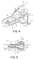
- Fig. 4 is a perspective view of first and second conductive contacts in the connector illustrated in Fig. 3; and
- Fig. 5 is a sectional view of the connector illustrated in Fig. 3 when the mating connector is coupled thereto.
-
- Now, description will be made of a connector according to an embodiment of this invention.
- Referring to Figs. 3 and 4, the connector is depicted by a
reference numeral 5 and comprises a switching contact 11 having a switching function, and aninsulator 41. The switching contact 11 comprises a firstconductive contact 21 and a secondconductive contact 31. - The
first contact 21 has a main orprimary spring portion 22, a subsidiary orsecondary spring portion 23, abent portion 24 connecting one ends of the main and thesubsidiary spring portions first holding portion 29 connected to the other end of thesubsidiary spring portion 23, and afirst terminal portion 30 extending from thefirst holding portion 29 to the outside of theinsulator 41. Thefirst contact 21 may be produced by punching and bending a single conductive plate. In this event, a combination of themain spring portion 22, thesubsidiary spring portion 23, and thebent portion 24 forms a generally U-shaped profile in a side view. - The
bent portion 24 is provided with anopening portion 25. Themain spring portion 22 has an operating portion or a contactingportion 26 protruding from its one end into theopening portion 25, afulcrum portion 27 formed at an intermediate position of themain spring portion 22, and a firstswitching contact point 28 formed at a rear part extending from thefulcrum portion 27 to the other end. It is noted here that the distance from thefulcrum portion 27 to the firstswitching contact point 28 is greater than the distance from thefulcrum portion 27 to the contactingportion 26. - The
insulator 41 has a receiving portion 43 receiving and holding the switching contact 11, aninsertion hole 41 a formed in afront wall portion 41c of theopening portion 25, and acontact insert hole 41 b formed on a rear side. Themain spring portion 22 is faced to onewall portion 43a of the receiving portion 43. Thesubsidiary spring portion 23 is faced to theother wall portion 43b of the receiving portion 43 which is opposite to the onewall portion 43a. The firstswitching contact point 28 is faced to thefirst holding portion 29. Thefirst holding portion 29 is held by theother wall portion 43b. - The
opening portion 25 serves to allow reception of amating contact 53 of amating connector 51 inserted from the outside of thebent portion 24 to an area between the main and thesubsidiary spring portions mating connector 51 is coupled to theconnector 5. Theopening portion 25 further extends towards thesubsidiary spring portion 23. - The contacting
portion 26 is brought into contact with themating contact 53 when themating connector 51 is coupled to theconnector 5. As a consequence, the main and thesubsidiary spring portions mating contact 53 to be moved towards the onewall portion 43a. - The
fulcrum portion 27 is supported by the onewall portion 43a. A front part of themain spring portion 22 extending from thefulcrum portion 27 to the contactingportion 26 is inclined to be gradually apart from the onewall portion 43a towards the contactingportion 26. The rear part of themain spring portion 22 from thefulcrum portion 27 to the other end extends along the onewall portion 43a. Thebent portion 24 urges themain spring portion 22 in a first direction (in Fig. 3, counterclockwise with respect to the fulcrum portion 27) to bring the firstswitching contact point 28 into contact with a secondswitching contact point 38 which will later be described. The most part of themain spring portion 22 can be considered as a seesaw portion capable of performing with respect to the fulcrum portion 27 a seesaw movement in a predetermined direction, namely, the first direction and a second direction reverse to the first direction. - The
second contact 31 comprises asecond holding portion 32 of a flat shape, aholding member 33, the secondswitching contact point 38, and asecond terminal portion 39. Thesecond holding portion 32 is inserted through thecontact insert hole 41 b of theinsulator 41 towards thefront wall portion 41c to be partially press fit into theinsulator 41 and thereby held by theinsulator 41. Theholding member 33 is bent from a flat plane of thesecond holding portion 32 to be perpendicular thereto and is held by theinsulator 41. The secondswitching contact point 38 is formed at a position faced to the firstswitching contact point 28 in the predetermined direction. Thesecond terminal portion 39 extends from the secondswitching contact point 38 to the outside of theinsulator 41. - The second
switching contact point 38 is located adjacent the onewall portion 43a. When theconnector 5 is not coupled to themating connector 51, the first and the secondswitching contact points - The switching contact 11 of the above-mentioned structure is turned on and off when the
connector 5 is coupled to and released from themating connector 51. - Next, description will be made of a coupling operation of the
connector 5 and themating connector 51 and a behavior of the switching contact 11 upon coupling. - When the
mating connector 51 is not coupled to theconnector 5 as illustrated in Fig. 3, the firstswitching contact point 28 and the secondswitching contact point 38 are kept in contact with each other. At an initial stage of the coupling, themating contact 53 passes through theinsertion hole 41 a to be inserted into the openingportion 25. At this time, themating contact 53 is brought into contact with the contactingportion 26 of thefirst contact 21. As a consequence, themating contact 53 presses and displaces the contactingportion 26 in an upward direction (depicted by an arrow A in Fig. 5). Specifically, themating contact 51 presses the contactingportion 26 in the second direction (in Fig. 3, clockwise with respect to the fulcrum portion 27) to make themain spring portion 22 perform the seesaw movement in the second direction. Simultaneously, the main and thesubsidiary spring portions switching contact point 28 is displaced in a downward direction (depicted by an arrow B in Fig. 5) under a lever action around thefulcrum portion 27 to be separated from the secondswitching contact point 38. - Eventually, as illustrated in Fig. 5, the front part from the
fulcrum portion 27 to the contactingportion 26 is located to extend along the onewall portion 43a while the rear part from thefulcrum portion 27 to the other end is inclined to be gradually apart from the onewall portion 43a towards the other end. In this state, a space or a contact point gap G1 is formed between the first and the second switching contact points 28 and 38. On the other hand, themating contact 53 is brought into contact with the contactingportion 26 of thefirst contact 21. Therefore, electrical circuit connection is switched from an initial state into a switched state. Since the openingportion 25 extends from thebent portion 24 to thesubsidiary spring portion 23, the openingportion 25 also serves to escape themating contact 53 to be inserted upon coupling. - When the
mating contact 53 is released from the switching contact 11, themain spring portion 22 performs the seesaw movement in the first direction to bring the firstswitching contact point 28 into contact with the secondswitching contact point 38 as illustrated in Fig. 3. Thus, the electrical circuit connection is recovered into the initial state. - In the above-mentioned connector, the first and the second switching contact points 28 and 38 are located at positions sufficiently apart from a contacting position of the contacting
portion 26 of thefirst contact 21 and themating contact 51. Therefore, it is possible to reduce the possibility of improper or insufficient contact between the first and the second switching contact points 28 and 38 due to the attachment of dust or the like. Since the openingportion 25 also serves to escape themating contact 21 to be inserted upon coupling, it is unnecessary to reserve a large mutual distance between the main and thesubsidiary spring portions first contact 21 can be reduced. Accordingly, the height of the connector as a whole can be reduced. In addition, the contact point gap G1 can be freely adjusted by selecting the position of thefulcrum portion 27. Therefore, the contact point gap G1 can be determined irrespective of the size of themating contact 51. Accordingly, a highly reliable connector with a switching function can be realized. - In the foregoing, description has been directed to the case where the first and the second switching contact points 28 and 38 are kept in contact with each other when the
mating connector 51 is not coupled to theconnector 5. It is possible to adopt an alternative switching arrangement such that the first and the second switching contact points 28 and 38 are out of contact from each other when mating connector is not coupled to theconnector 51. - By selecting the position of the
fulcrum portion 27 at any given position in the longitudinal direction of themain spring portion 22, the contact point gap G1 can be adjusted as desired. Thesecond contact 31 can be formed by punching and bending a thin conductive plate in the manner similar to thefirst contact 21. Furthermore, theinsulator 41 may be covered with a thin metal shell which can be used as a ground.
Claims (8)
- A connector with a switching function, comprising first and second conductive contacts adapted to be brought into contact with and released from each other, and an insulator holding said first and said second conductive contacts, characterized in that said first conductive contact comprises a seesaw portion supported by said insulator to be movable in a seesaw movement in a predetermined direction, an operating portion formed at one end of said seesaw portion to be operated by a mating contact in said predetermined direction, and a contact point formed at the other end of said seesaw portion and faced to said second conductive contact in said predetermined direction.
- The connector according to claim 1, wherein said seesaw portion is urged to make said contacting point be brought into contact with said second conductive contact in a first direction of said predetermined direction.
- The connector according to claim 2, wherein said mating contact is for pressing said operating portion in a second direction reverse to said first direction.
- The connector according to claim 3, wherein said mating contact has a conductivity.
- The connector according to claim 4, wherein said insulator has a receiving portion receiving said first and said second conductive contacts, said first conductive contact comprising a main spring portion serving as said seesaw portion and faced to one wall portion of said receiving portion, a subsidiary spring portion faced to the other wall portion of said receiving portion opposite to said one wall portion, and a bent portion connecting one ends of said main and said subsidiary spring portions, said bent portion having an opening portion for receiving said mating contact to be inserted from the outside of said bent portion to an area between said main and said subsidiary spring portions.
- The connector according to claim 5, wherein said main spring portion has a contacting portion serving as said operating portion and protruding from one end of said main spring portion to said opening portion, a fulcrum portion formed at an intermediate position of said main spring portion and supported by said one wall portion, and a first switching contact point serving as said contact point and extending from said fulcrum portion towards the other end, said second conductive contact having a second switching contact point formed at a position faced to said first switching contact point.
- The connector according to claim 6, wherein said first conductive contact has a holding portion connected to the other end of said subsidiary spring portion, said holding portion being held by said other wall portion, said first switching contact point being faced to said holding portion, said second switching contact point being located adjacent to said one wall portion, said first and said second switching contact points being kept in contact with each other when said mating contact does not operate said operating portion.
- The connector according to claim 6, wherein said opening portion further extends in said subsidiary spring portion towards said holding portion.
Applications Claiming Priority (2)
| Application Number | Priority Date | Filing Date | Title |
|---|---|---|---|
| JP2000233434A JP3427377B2 (en) | 2000-08-01 | 2000-08-01 | Connector with switch function |
| JP2000233434 | 2000-08-01 |
Publications (2)
| Publication Number | Publication Date |
|---|---|
| EP1178575A1 true EP1178575A1 (en) | 2002-02-06 |
| EP1178575B1 EP1178575B1 (en) | 2005-05-04 |
Family
ID=18725953
Family Applications (1)
| Application Number | Title | Priority Date | Filing Date |
|---|---|---|---|
| EP01117535A Expired - Lifetime EP1178575B1 (en) | 2000-08-01 | 2001-07-20 | Connector with a switching function |
Country Status (6)
| Country | Link |
|---|---|
| EP (1) | EP1178575B1 (en) |
| JP (1) | JP3427377B2 (en) |
| KR (1) | KR100427855B1 (en) |
| CN (1) | CN1149720C (en) |
| AU (1) | AU783927B2 (en) |
| DE (1) | DE60110507T2 (en) |
Cited By (3)
| Publication number | Priority date | Publication date | Assignee | Title |
|---|---|---|---|---|
| EP1930996A1 (en) * | 2006-12-08 | 2008-06-11 | Electrolux Home Products Corporation N.V. | A safety device for household ovens |
| CN107112676A (en) * | 2014-12-30 | 2017-08-29 | 吉伯生品牌公司 | Many contact sockets |
| CN109417253A (en) * | 2016-06-23 | 2019-03-01 | 浩亭电子有限公司 | Electric conductor connecting element |
Citations (5)
| Publication number | Priority date | Publication date | Assignee | Title |
|---|---|---|---|---|
| US5338215A (en) * | 1993-03-19 | 1994-08-16 | Molex Incorporated | Jack assembly including a contact switching system |
| US5743760A (en) * | 1995-09-25 | 1998-04-28 | Yazaki Corporation | Connector engagement detecting device |
| EP0895742A1 (en) * | 1997-08-04 | 1999-02-10 | Seb S.A. | Connection device for portable apparatus |
| US5914846A (en) * | 1997-05-06 | 1999-06-22 | Tii Industries, Inc. | Cable interconnection apparatus for network interface device |
| US6062885A (en) * | 1999-04-23 | 2000-05-16 | Molex Incorporated | Electrical switch assembly |
Family Cites Families (5)
| Publication number | Priority date | Publication date | Assignee | Title |
|---|---|---|---|---|
| JPS59134385U (en) * | 1983-02-28 | 1984-09-08 | 株式会社ジヤルコ | jack |
| JPS61186183U (en) * | 1985-05-13 | 1986-11-20 | ||
| JPH024460Y2 (en) * | 1986-12-27 | 1990-02-01 | ||
| FR2681733B1 (en) * | 1991-09-19 | 1993-12-10 | Souriau Cie | FEMALE CONTACT WITH ELASTIC PALLET AND PALLET FOR SUCH A CONTACT. |
| US5562486A (en) * | 1993-04-21 | 1996-10-08 | Sumitomo Wiring Systems, Ltd. | Lock detection connector |
-
2000
- 2000-08-01 JP JP2000233434A patent/JP3427377B2/en not_active Expired - Fee Related
-
2001
- 2001-07-10 AU AU54293/01A patent/AU783927B2/en not_active Ceased
- 2001-07-16 CN CNB011206136A patent/CN1149720C/en not_active Expired - Fee Related
- 2001-07-20 DE DE60110507T patent/DE60110507T2/en not_active Expired - Lifetime
- 2001-07-20 EP EP01117535A patent/EP1178575B1/en not_active Expired - Lifetime
- 2001-08-01 KR KR10-2001-0046559A patent/KR100427855B1/en not_active Expired - Fee Related
Patent Citations (5)
| Publication number | Priority date | Publication date | Assignee | Title |
|---|---|---|---|---|
| US5338215A (en) * | 1993-03-19 | 1994-08-16 | Molex Incorporated | Jack assembly including a contact switching system |
| US5743760A (en) * | 1995-09-25 | 1998-04-28 | Yazaki Corporation | Connector engagement detecting device |
| US5914846A (en) * | 1997-05-06 | 1999-06-22 | Tii Industries, Inc. | Cable interconnection apparatus for network interface device |
| EP0895742A1 (en) * | 1997-08-04 | 1999-02-10 | Seb S.A. | Connection device for portable apparatus |
| US6062885A (en) * | 1999-04-23 | 2000-05-16 | Molex Incorporated | Electrical switch assembly |
Cited By (8)
| Publication number | Priority date | Publication date | Assignee | Title |
|---|---|---|---|---|
| EP1930996A1 (en) * | 2006-12-08 | 2008-06-11 | Electrolux Home Products Corporation N.V. | A safety device for household ovens |
| EP2100079A4 (en) * | 2006-12-08 | 2009-12-30 | Electrolux Home Prod Corp | A safety device for household ovens |
| CN107112676A (en) * | 2014-12-30 | 2017-08-29 | 吉伯生品牌公司 | Many contact sockets |
| EP3241258A4 (en) * | 2014-12-30 | 2018-06-20 | Gibson Brands, Inc. | Multiple contact jack |
| CN107112676B (en) * | 2014-12-30 | 2019-12-03 | 吉伯生品牌公司 | multi-contact socket |
| GB2548517B (en) * | 2014-12-30 | 2021-09-01 | Gibson Brands Inc | Multiple contact jack |
| CN109417253A (en) * | 2016-06-23 | 2019-03-01 | 浩亭电子有限公司 | Electric conductor connecting element |
| CN109417253B (en) * | 2016-06-23 | 2021-03-16 | 浩亭电子有限公司 | Electrical conductor connecting element |
Also Published As
| Publication number | Publication date |
|---|---|
| JP3427377B2 (en) | 2003-07-14 |
| CN1335655A (en) | 2002-02-13 |
| AU783927B2 (en) | 2005-12-22 |
| CN1149720C (en) | 2004-05-12 |
| KR100427855B1 (en) | 2004-04-27 |
| DE60110507T2 (en) | 2006-02-23 |
| JP2002050439A (en) | 2002-02-15 |
| EP1178575B1 (en) | 2005-05-04 |
| KR20020011349A (en) | 2002-02-08 |
| DE60110507D1 (en) | 2005-06-09 |
| AU5429301A (en) | 2002-02-07 |
Similar Documents
| Publication | Publication Date | Title |
|---|---|---|
| US3903385A (en) | Shorting bar switch in electrical connector biasing assembly | |
| EP1507316B1 (en) | Connection terminal | |
| US4838816A (en) | Electrical terminal having a receptacle contact section of low insertion force | |
| US6231396B1 (en) | Jack connector | |
| JP3250787B2 (en) | Locking device for electrical connector | |
| KR100264848B1 (en) | Socket type contacts and electrical connectors using the same | |
| EP1635425B1 (en) | Connection terminal | |
| US6322397B1 (en) | Miniaturized power jack with high normal force | |
| US20070218774A1 (en) | Audio jack with improved contact arrangement | |
| HK1042990B (en) | Connector excellent in reliability of contact | |
| JPH07192795A (en) | Female electrical terminal | |
| US5693924A (en) | Switching contact mechanism with wipe and backwipe | |
| US6319030B1 (en) | Switching receptacle connector | |
| US7094088B2 (en) | Electrical connector having improved connection | |
| US6929491B1 (en) | Card connector | |
| EP1178575B1 (en) | Connector with a switching function | |
| US5697813A (en) | Connection terminal | |
| US6364717B1 (en) | Audio jack with a controlled normal force for retaining a mating plug | |
| EP1014405A2 (en) | Push switch | |
| JPH0212394B2 (en) | ||
| US7371126B2 (en) | Electrical connector with position means | |
| JP3268384B2 (en) | connector | |
| US20040238341A1 (en) | Tact switch | |
| JP3460060B2 (en) | Socket contact | |
| JP2596876Y2 (en) | Coaxial connector |
Legal Events
| Date | Code | Title | Description |
|---|---|---|---|
| PUAI | Public reference made under article 153(3) epc to a published international application that has entered the european phase |
Free format text: ORIGINAL CODE: 0009012 |
|
| AK | Designated contracting states |
Kind code of ref document: A1 Designated state(s): AT BE CH CY DE DK ES FI FR GB GR IE IT LI LU MC NL PT SE TR Kind code of ref document: A1 Designated state(s): DE FI FR GB SE |
|
| AX | Request for extension of the european patent |
Free format text: AL;LT;LV;MK;RO;SI |
|
| 17P | Request for examination filed |
Effective date: 20020802 |
|
| AKX | Designation fees paid |
Free format text: DE FI FR GB SE |
|
| GRAH | Despatch of communication of intention to grant a patent |
Free format text: ORIGINAL CODE: EPIDOS IGRA |
|
| GRAH | Despatch of communication of intention to grant a patent |
Free format text: ORIGINAL CODE: EPIDOS IGRA |
|
| 17Q | First examination report despatched |
Effective date: 20030422 |
|
| GRAA | (expected) grant |
Free format text: ORIGINAL CODE: 0009210 |
|
| AK | Designated contracting states |
Kind code of ref document: B1 Designated state(s): DE FI FR GB SE |
|
| REG | Reference to a national code |
Ref country code: GB Ref legal event code: FG4D |
|
| REG | Reference to a national code |
Ref country code: SE Ref legal event code: TRGR |
|
| REG | Reference to a national code |
Ref country code: IE Ref legal event code: FG4D |
|
| REF | Corresponds to: |
Ref document number: 60110507 Country of ref document: DE Date of ref document: 20050609 Kind code of ref document: P |
|
| PGFP | Annual fee paid to national office [announced via postgrant information from national office to epo] |
Ref country code: FR Payment date: 20050728 Year of fee payment: 5 |
|
| ET | Fr: translation filed | ||
| PLBE | No opposition filed within time limit |
Free format text: ORIGINAL CODE: 0009261 |
|
| STAA | Information on the status of an ep patent application or granted ep patent |
Free format text: STATUS: NO OPPOSITION FILED WITHIN TIME LIMIT |
|
| 26N | No opposition filed |
Effective date: 20060207 |
|
| PGFP | Annual fee paid to national office [announced via postgrant information from national office to epo] |
Ref country code: GB Payment date: 20060705 Year of fee payment: 6 Ref country code: SE Payment date: 20060705 Year of fee payment: 6 |
|
| EUG | Se: european patent has lapsed | ||
| GBPC | Gb: european patent ceased through non-payment of renewal fee |
Effective date: 20070720 |
|
| PG25 | Lapsed in a contracting state [announced via postgrant information from national office to epo] |
Ref country code: SE Free format text: LAPSE BECAUSE OF NON-PAYMENT OF DUE FEES Effective date: 20070721 |
|
| PG25 | Lapsed in a contracting state [announced via postgrant information from national office to epo] |
Ref country code: GB Free format text: LAPSE BECAUSE OF NON-PAYMENT OF DUE FEES Effective date: 20070720 |
|
| REG | Reference to a national code |
Ref country code: FR Ref legal event code: ST Effective date: 20080331 |
|
| PG25 | Lapsed in a contracting state [announced via postgrant information from national office to epo] |
Ref country code: FR Free format text: LAPSE BECAUSE OF NON-PAYMENT OF DUE FEES Effective date: 20070731 |
|
| PG25 | Lapsed in a contracting state [announced via postgrant information from national office to epo] |
Ref country code: FR Free format text: LAPSE BECAUSE OF NON-PAYMENT OF DUE FEES Effective date: 20060731 |
|
| PGFP | Annual fee paid to national office [announced via postgrant information from national office to epo] |
Ref country code: FI Payment date: 20170710 Year of fee payment: 17 Ref country code: DE Payment date: 20170711 Year of fee payment: 17 |
|
| REG | Reference to a national code |
Ref country code: DE Ref legal event code: R119 Ref document number: 60110507 Country of ref document: DE |
|
| PG25 | Lapsed in a contracting state [announced via postgrant information from national office to epo] |
Ref country code: FI Free format text: LAPSE BECAUSE OF NON-PAYMENT OF DUE FEES Effective date: 20180720 Ref country code: DE Free format text: LAPSE BECAUSE OF NON-PAYMENT OF DUE FEES Effective date: 20190201 |