EP1176712A2 - Variable gain amplifier - Google Patents
Variable gain amplifier Download PDFInfo
- Publication number
- EP1176712A2 EP1176712A2 EP01110438A EP01110438A EP1176712A2 EP 1176712 A2 EP1176712 A2 EP 1176712A2 EP 01110438 A EP01110438 A EP 01110438A EP 01110438 A EP01110438 A EP 01110438A EP 1176712 A2 EP1176712 A2 EP 1176712A2
- Authority
- EP
- European Patent Office
- Prior art keywords
- transistor
- variable gain
- capacitor
- current
- gain
- Prior art date
- Legal status (The legal status is an assumption and is not a legal conclusion. Google has not performed a legal analysis and makes no representation as to the accuracy of the status listed.)
- Withdrawn
Links
- 239000003990 capacitor Substances 0.000 claims abstract description 20
- 238000010586 diagram Methods 0.000 description 6
- 230000003321 amplification Effects 0.000 description 5
- 238000003199 nucleic acid amplification method Methods 0.000 description 5
- 230000008878 coupling Effects 0.000 description 2
- 238000010168 coupling process Methods 0.000 description 2
- 238000005859 coupling reaction Methods 0.000 description 2
- 230000009977 dual effect Effects 0.000 description 1
- 238000010295 mobile communication Methods 0.000 description 1
- 230000003071 parasitic effect Effects 0.000 description 1
Images



Classifications
-
- H—ELECTRICITY
- H03—ELECTRONIC CIRCUITRY
- H03G—CONTROL OF AMPLIFICATION
- H03G3/00—Gain control in amplifiers or frequency changers
-
- H—ELECTRICITY
- H03—ELECTRONIC CIRCUITRY
- H03G—CONTROL OF AMPLIFICATION
- H03G1/00—Details of arrangements for controlling amplification
- H03G1/0005—Circuits characterised by the type of controlling devices operated by a controlling current or voltage signal
- H03G1/0017—Circuits characterised by the type of controlling devices operated by a controlling current or voltage signal the device being at least one of the amplifying solid-state elements
- H03G1/0023—Circuits characterised by the type of controlling devices operated by a controlling current or voltage signal the device being at least one of the amplifying solid-state elements in emitter-coupled or cascode amplifiers
Definitions
- the present invention relates to a variable gain amplifier and particularly to a variable gain amplifier which includes a parallel connection of a resistance and a capacitor, or a parallel connection of an inductance and a capacitor.
- Cascade amplifiers are employed for amplifying radio frequency signals for the pocket telephones and information terminals. Further, the cascade amplifiers are often provided with means for obtaining variable gain.
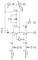
- FIG. 4 is a block diagram of a conventional variable gain cascade amplifier.
- the amplifier as shown in Figure 4 comprises a cascade amplifier including common-emitter transistor Q0 and common-base transistor Q1, a variable gain unit including transistor Q2 and Q3 and resistance R2, resistance R0 for applying bias V3 to the base of transistor Q0, resistance R1 for the load resistance of the cascade amplifier, voltage supply V2 for the amplifier as a whole, voltage supply V0 (voltage supply 50) for controlling the gain of the variable gain unit, signal input terminal 10, signal output terminal 40, power supplies and coupling capacitors connected with signal input terminal 10 and signal output terminal 40, respectively.
- V0 voltage supply 50
- the variable gain cascade amplifier as shown in Figure 4 obtains the variable gain by varying V0 so as to change the route of current which flows into transistor Q0. Concretely, the amplification gain becomes low, when V0 is greater than V1, because the current flows via transistors Q2 and Q3 into transistor Q0, while the amplification gain becomes high, when V0 is smaller than V1, because the current flows via transistor Q1 into transistor Q0.
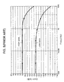
- Figure 5 is a graph of a frequency characteristics of the conventional variable gain cascade amplifier as shown in Figure 4.
- the cut off frequency at the high gain state is about 4 GHz, while the cut off frequency at the low gain state is about 1.5 GHz, as shown in Figure 5.
- the cut off frequency at the high gain state is different from that at the low gain state, because the impedance of the base of transistor Q2 is high due to resistance R2 at higher frequency, and CR circuit by resistance R2 and parasitic capacitance C between the base and the collector of transistor Q2 limits the frequency characteristics. Therefore, the frequency characteristics varies, as the gain varies, in the conventional variable gain amplifier.
- An object of the present invention is to provide a variable gain amplifier wherein the frequency characteristics is unchanged, when the gain is changed.
- the variable gain amplifier of the present invention comprises an amplifying unit for amplifying an inputted signal and a variable gain unit for varying the gain of the amplifying unit.
- the variable gain unit includes a transistor and a parallel connection of a resistor and a capacitor connected with the transistor.
- the variable gain unit may includes a transistor and a parallel connection of a resistor and an inductance.
- the impedance of the base of the transistor is lowered by the parallel connection of a resistance and a capacitor in higher frequency range.
- variable gain amplifier of the present invention are applied for various electronic appliances such as pocket telephones.
- variable gain amplifier of present invention the frequency characteristics remain unchanged, because the impedance of the control electrode such as a base or a gate of amplifying transistor are made low in higher frequency range, by using a parallel connection of a resistance (or inductance) and a capacitance connected with the control electrode of the amplifying transistor.
- FIG. 1 is a block diagram of the variable gain amplifier of the present invention.
- FIG. 2 is a circuit diagram of the variable gain amplifier of the present invention as shown in FIG. 1.
- FIG. 3 is a graph for showing the cut off frequency of the variable gain amplifier of the present invention as shown in FIG. 2.
- FIG. 4 is a block diagram of a conventional variable gain amplifier.
- FIG. 5 is a graph for showing the cut off frequency of the conventional variable gain amplifier as shown in FIG. 4.
- Figure 1 is a block diagram of the variable gain amplifier of the present invention. There are shown in Figure 1 input port 10 (PORT0) for inputting a signal, amplifying unit for amplifying the signal from input port 10, variable gain unit 30 for varying the amplification gain of amplifying unit 20, voltage supply 50 (V0) for variable gain unit 30, and output port 40 for outputting the amplified signal.
- input port 10 PORT0
- amplifying unit for amplifying the signal from input port
- variable gain unit 30 for varying the amplification gain of amplifying unit
- V0 voltage supply 50
- V0 variable gain unit 30
- output port 40 for outputting the amplified signal.
- FIG 2 is a circuit diagram of the variable gain amplifier as shown in Figure 1.
- Amplifying unit 20 as shown in Figure 1 is a cascade amplifier which includes common-emitter transistor Q0 and common base transistor Q1.
- variable gain unit 30 as shown in Figure 1 includes transistors Q2 and Q3, resistor R2 and capacitor C2.
- resistance R0 for applying DC bias V3 to the base of transistor Q0 Resistor R1 as a load resistance for the cascade amplifier, voltage supply V1 for biasing the base of transistor Q1, voltage supply V2 for the variable gain amplifier of the present invention as a whole, input port 10, output terminal 40, and power supplies and coupling capacitors connected with input port 10 and output port 40.
- Resistance R2 may be replaced by inductance L, and bipolar transistors may be replaced by other types such MOS transistors.
- the electrode for controlling the transistors are the bases of the bipolar transistors, or gates of the MOS transistors.
- Resistance R2 gives a current feedback for transistor Q2, thereby lowering the mutual conductance "gm” of transistor Q2, and limiting the current flowing from voltage supply V0.
- the emitter area ratio (the emitter area of transistor Q2 : the emitter area of Q3) made to be 1: n where "n" is greater than or equal to 1, thereby controlling each current.
- Capacitor C2 is connected in parallel with R2 connected with the base of transistor Q2 is a bypass capacitor for lowering the impedance of the base of transistor Q2 in higher frequency range.
- Capacitor C2 is a peaking capacitor, because it improves the high frequency characteristics.
- the current of the cascade amplifier by voltage V2 flows through R1.
- the base of transistor Q1 is biased by voltage supply V1. while transistor Q2 is turned off. Therefore, the current flows through R1 and Q1 into transistor Q0.
- transistor Q0 flows into the earth (GND) connected with the emitter of transistor Q0, because transistor Q0 becomes a constant current DC current source due to the bias of its base. Therefore, when voltage Vo is lower than voltage V1, the signal inputted from PORT0 is amplified with the gain of the cascade amplifier itself.
- transistor Q3 is turned on by voltage V0, and the current by voltage V2 flows into transistor Q0 via transistor Q3. Further, the current through resistance R1 by voltage V2 flows also into transistor Q0 via transistor Q2, because transistor Q1 is turned off.
- the current through transistor Q2 varies the gain of the cascade amplifier, because it depends upon the load current through load resistance R1 of the cascade amplifier.
- the current through transistor Q2 added to the current through Transistor Q3 becomes the current through transistor Q0.
- the current through transistor Q2 added to the current through transistor Q3 flows via transistor Q0 into the earth (GND) connected with the emitter of transistor Q0, because transistor Q0 becomes a constant current DC current source due to the bias of its base. Therefore, when voltage Vo is higher than voltage V1, the signal inputted from PORT0 is amplified with the gain controlled by the variable gain unit including transistors Q2 and Q3.
- the current through Q2 is smaller than the current through Q1 in order to obtain the higher gain when V0 is lower than V1 and to obtain the lower gain when V0 is higher than V1.
- Figure 3 is a graph of a frequency characteristic of the variable gain amplifier of the present invention as shown in Figure 2.
- the cut off frequency is about 4 GHz both at the high gain and at the low gain, as shown in Figure 3, thereby broadening the frequency characteristics regardless of the amplification gain.
- the present invention is applicable to a low niose amplifier wherein an emitter of a common-emitter transistor is not connected with a resister, because the amplification gain is controlled by a base of a common-base transistor. Further, the present invention is applicable to a mixer, antenna switch.
- variable gain amplifier of the present invention is applicable to a dual band pocket telephone suc as GSM (global system for mobile communication), because 800 MHz and 1.9 GHz signals are received by using a single amplifier.
- GSM global system for mobile communication
Landscapes
- Control Of Amplification And Gain Control (AREA)
- Amplifiers (AREA)
- Networks Using Active Elements (AREA)
Abstract
Description
Claims (5)
- A variable gain amplifier which comprises an amplifying unit for amplifying an inputted signal and a variable gain unit for varying a gain of said amplifying unit,
wherein said variable gain unit includes a transistor connected with a parallel connection of a capacitor and a resistor, or connected with a parallel connection of a capacitor and an inductance,
wherein:said gain is made high by turning off said variable gain unit, while said gain is made low by turning on said variable gain unit; andthe cut off frequency is unchanged, regardless of said gain. - The variable gain amplifier according to claim 1, wherein said cascade amplifier comprises:a first transistor Q1 which is turned on or off by said variable gain unit; anda second transistor Q0 which is connected in cascade with said first transistor, andsaid variable gain unit comprises:a third transistor Q2 connected with said Q1;a parallel connection of a capacitor and a resistor one of which end is connected with said Q2, or a parallel connection of a capacitor and an inductance one of which end is connected with said Q2,; anda forth transistor Q3 connected with another end of said parallel connection,
wherein the current through Q2 is smaller than the current through Q1, andsaid Q2 and Q3 is turned off when said V1 is greater than said V0, while said Q2 and Q3 is turned on when said V1 is smaller than said V0. - The variable gain amplifier according to claim 2, wherein said Q1 and said Q2 are bipolar transistors, wherein the collector of said Q1 is connected with the collector of said Q2, while the emitter of said Q1 is connected with the emitter of said Q2.
- The variable gain amplifier according to claim 2, wherein said Q1 and said Q2 are MOS transistors, wherein the source of said Q1 is connected with the source of said Q2, while the drain of said Q1 is connected with the drain of said Q2.
- The variable gain amplifier according to claim 2, wherein both said Q2 and said Q3 are turned on or off by said voltage V0.
Applications Claiming Priority (2)
| Application Number | Priority Date | Filing Date | Title |
|---|---|---|---|
| JP2000222705A JP2002043875A (en) | 2000-07-24 | 2000-07-24 | Variable gain amplifier and electronic equipment provided with the same |
| JP2000222705 | 2000-07-24 |
Publications (2)
| Publication Number | Publication Date |
|---|---|
| EP1176712A2 true EP1176712A2 (en) | 2002-01-30 |
| EP1176712A3 EP1176712A3 (en) | 2003-12-17 |
Family
ID=18716914
Family Applications (1)
| Application Number | Title | Priority Date | Filing Date |
|---|---|---|---|
| EP01110438A Withdrawn EP1176712A3 (en) | 2000-07-24 | 2001-04-27 | Variable gain amplifier |
Country Status (4)
| Country | Link |
|---|---|
| US (1) | US6509798B2 (en) |
| EP (1) | EP1176712A3 (en) |
| JP (1) | JP2002043875A (en) |
| KR (1) | KR100425757B1 (en) |
Cited By (1)
| Publication number | Priority date | Publication date | Assignee | Title |
|---|---|---|---|---|
| CN107769740A (en) * | 2016-08-23 | 2018-03-06 | 株式会社村田制作所 | High-frequency amplifier module |
Families Citing this family (9)
| Publication number | Priority date | Publication date | Assignee | Title |
|---|---|---|---|---|
| JP4405113B2 (en) * | 2001-08-16 | 2010-01-27 | パナソニック株式会社 | Variable gain amplifier circuit |
| KR100468355B1 (en) * | 2002-11-25 | 2005-01-27 | 인티그런트 테크놀로지즈(주) | Circuit for Controlling Slope and Offset of Gain Curve of Variable Gain Amplifier |
| TW200505157A (en) * | 2003-07-21 | 2005-02-01 | Realtek Semiconductor Corp | Linear-in-decibel variable gain amplifier |
| US7075368B2 (en) * | 2003-09-01 | 2006-07-11 | Realtek Semiconductor Corp. | Linear-in-decibel variable gain amplifier |
| US7078972B2 (en) * | 2003-10-01 | 2006-07-18 | Realtek Semiconductor Corp. | Linear decibel-scale variable gain amplifier |
| KR100857223B1 (en) | 2007-02-28 | 2008-09-05 | 충북대학교 산학협력단 | Variable gain amplifier |
| US8633576B2 (en) | 2011-04-21 | 2014-01-21 | Tessera, Inc. | Stacked chip-on-board module with edge connector |
| KR101931256B1 (en) | 2012-07-25 | 2018-12-20 | 삼성전자주식회사 | Wireless power reception apparatus and method |
| CN103107789B (en) * | 2013-02-03 | 2015-12-02 | 北京工业大学 | The variable gain amplifier that a kind of common-mode feedback resistor shares |
Family Cites Families (13)
| Publication number | Priority date | Publication date | Assignee | Title |
|---|---|---|---|---|
| DE2262089C3 (en) * | 1972-12-19 | 1975-10-30 | Philips Patentverwaltung Gmbh, 2000 Hamburg | Circuit arrangement for electronic frequency influencing, in particular electronic sound adjuster |
| US4344043A (en) * | 1980-04-23 | 1982-08-10 | Rca Corporation | Variable load impedance gain-controlled amplifier |
| JPH0474010A (en) | 1990-07-13 | 1992-03-09 | Iwatsu Electric Co Ltd | Differential amplifier |
| DE4329896A1 (en) | 1993-09-04 | 1995-03-09 | Thomson Brandt Gmbh | Amplifier stage with a dB linear output voltage |
| JP3060981B2 (en) * | 1997-02-21 | 2000-07-10 | 日本電気株式会社 | Microwave amplifier |
| BR9703233A (en) * | 1997-05-30 | 1998-12-29 | Brasilia Telecom | Improvement introduced in transimpedance amplifier |
| US6046640A (en) * | 1997-11-07 | 2000-04-04 | Analog Devices, Inc. | Switched-gain cascode amplifier using loading network for gain control |
| EP0917285B1 (en) * | 1997-11-14 | 2003-05-07 | Zarlink Semiconductor Limited | Low-voltage amplifiers |
| US6628170B2 (en) * | 1998-06-04 | 2003-09-30 | Analog Devices, Inc. | Low noise amplifier |
| IT1305642B1 (en) * | 1998-06-23 | 2001-05-15 | St Microelectronics Srl | LOW-NOISE RF AMPLIFIER AT FREQUENCY AND PROGRAMMABLE GAIN |
| US5999056A (en) * | 1998-06-30 | 1999-12-07 | Philips Electronics North Amercia Corporation | Variable gain amplifier using impedance network |
| US6046641A (en) * | 1998-07-22 | 2000-04-04 | Eni Technologies, Inc. | Parallel HV MOSFET high power stable amplifier |
| US6249153B1 (en) * | 1999-05-25 | 2001-06-19 | Micrel Incorporated | High slew rate input differential pair with common mode input to ground |
-
2000
- 2000-07-24 JP JP2000222705A patent/JP2002043875A/en not_active Withdrawn
-
2001
- 2001-04-27 KR KR10-2001-0022958A patent/KR100425757B1/en not_active Expired - Fee Related
- 2001-04-27 EP EP01110438A patent/EP1176712A3/en not_active Withdrawn
- 2001-06-22 US US09/888,179 patent/US6509798B2/en not_active Expired - Fee Related
Cited By (1)
| Publication number | Priority date | Publication date | Assignee | Title |
|---|---|---|---|---|
| CN107769740A (en) * | 2016-08-23 | 2018-03-06 | 株式会社村田制作所 | High-frequency amplifier module |
Also Published As
| Publication number | Publication date |
|---|---|
| KR100425757B1 (en) | 2004-04-03 |
| JP2002043875A (en) | 2002-02-08 |
| US6509798B2 (en) | 2003-01-21 |
| US20020008582A1 (en) | 2002-01-24 |
| KR20020008746A (en) | 2002-01-31 |
| EP1176712A3 (en) | 2003-12-17 |
Similar Documents
| Publication | Publication Date | Title |
|---|---|---|
| KR100704568B1 (en) | Variable gain low noise amplifier | |
| KR102287445B1 (en) | System and method for bypassing a low noise amplifier | |
| US6724259B2 (en) | Variable gain amplifier | |
| CN101515784B (en) | Amplifier, attenuation module and method for attenuating radio frequency signals | |
| US6778016B2 (en) | Simple self-biased cascode amplifier circuit | |
| KR20020038498A (en) | High frequency power amplifier, wireless communication apparatus and wireless communication system | |
| KR20030011233A (en) | High frequency power amplifier circuit device | |
| US7224228B2 (en) | Semiconductor integrated circuit for high frequency power amplifier, electronic component for high frequency power amplifier, and radio communication system | |
| KR20050027993A (en) | Switchable gain amplifier | |
| US6144254A (en) | Low-noise amplifier with switched gain and method | |
| US5844443A (en) | Linear high-frequency amplifier with high input impedance and high power efficiency | |
| KR20020076115A (en) | Rf variable gain amplifying device | |
| US6509798B2 (en) | Variable gain amplifier | |
| JP2003060456A (en) | Variable gain amplifier circuit | |
| US7400192B2 (en) | Low noise amplifier and differential amplifier with variable gain mode | |
| US6778019B2 (en) | Method and device for biasing a transistor of a radio frequency amplifier stage | |
| US5973543A (en) | Bias circuit for bipolar transistor | |
| US8115552B2 (en) | Amplifier circuit with step gain | |
| US6100763A (en) | Circuit for RF buffer and method of operation | |
| EP2045913A1 (en) | Low noise amplifier and N-mode gain control circuit therefor | |
| US7541876B2 (en) | Amplifier and method for operating the same | |
| US20030058045A1 (en) | Power control in RF amplifiers | |
| US20260045917A1 (en) | Amplifier circuit | |
| JPH0548348A (en) | Power amplifier circuit | |
| US9407220B1 (en) | Digitally controlled variable transductance stage for microwave mixers and amplifiers |
Legal Events
| Date | Code | Title | Description |
|---|---|---|---|
| PUAI | Public reference made under article 153(3) epc to a published international application that has entered the european phase |
Free format text: ORIGINAL CODE: 0009012 |
|
| AK | Designated contracting states |
Kind code of ref document: A2 Designated state(s): AT BE CH CY DE DK ES FI FR GB GR IE IT LI LU MC NL PT SE TR |
|
| AX | Request for extension of the european patent |
Free format text: AL;LT;LV;MK;RO;SI |
|
| RAP1 | Party data changed (applicant data changed or rights of an application transferred) |
Owner name: NEC COMPOUND SEMICONDUCTOR DEVICES, LTD. |
|
| PUAL | Search report despatched |
Free format text: ORIGINAL CODE: 0009013 |
|
| AK | Designated contracting states |
Kind code of ref document: A3 Designated state(s): AT BE CH CY DE DK ES FI FR GB GR IE IT LI LU MC NL PT SE TR |
|
| AX | Request for extension of the european patent |
Extension state: AL LT LV MK RO SI |
|
| RIC1 | Information provided on ipc code assigned before grant |
Ipc: 7H 03F 1/22 B Ipc: 7H 03G 1/00 A |
|
| 17P | Request for examination filed |
Effective date: 20031103 |
|
| 17Q | First examination report despatched |
Effective date: 20040709 |
|
| AKX | Designation fees paid |
Designated state(s): DE FR |
|
| STAA | Information on the status of an ep patent application or granted ep patent |
Free format text: STATUS: THE APPLICATION HAS BEEN WITHDRAWN |
|
| 18W | Application withdrawn |
Effective date: 20050603 |