EP1175010A1 - High frequency oscillator - Google Patents
High frequency oscillator Download PDFInfo
- Publication number
- EP1175010A1 EP1175010A1 EP01114626A EP01114626A EP1175010A1 EP 1175010 A1 EP1175010 A1 EP 1175010A1 EP 01114626 A EP01114626 A EP 01114626A EP 01114626 A EP01114626 A EP 01114626A EP 1175010 A1 EP1175010 A1 EP 1175010A1
- Authority
- EP
- European Patent Office
- Prior art keywords
- oscillator
- phase
- high frequency
- ghz
- delay cell
- Prior art date
- Legal status (The legal status is an assumption and is not a legal conclusion. Google has not performed a legal analysis and makes no representation as to the accuracy of the status listed.)
- Granted
Links
Images


Classifications
-
- H—ELECTRICITY
- H03—ELECTRONIC CIRCUITRY
- H03L—AUTOMATIC CONTROL, STARTING, SYNCHRONISATION, OR STABILISATION OF GENERATORS OF ELECTRONIC OSCILLATIONS OR PULSES
- H03L7/00—Automatic control of frequency or phase; Synchronisation
- H03L7/06—Automatic control of frequency or phase; Synchronisation using a reference signal applied to a frequency- or phase-locked loop
- H03L7/08—Details of the phase-locked loop
- H03L7/085—Details of the phase-locked loop concerning mainly the frequency- or phase-detection arrangement including the filtering or amplification of its output signal
- H03L7/087—Details of the phase-locked loop concerning mainly the frequency- or phase-detection arrangement including the filtering or amplification of its output signal using at least two phase detectors or a frequency and phase detector in the loop
-
- H—ELECTRICITY
- H03—ELECTRONIC CIRCUITRY
- H03L—AUTOMATIC CONTROL, STARTING, SYNCHRONISATION, OR STABILISATION OF GENERATORS OF ELECTRONIC OSCILLATIONS OR PULSES
- H03L7/00—Automatic control of frequency or phase; Synchronisation
- H03L7/06—Automatic control of frequency or phase; Synchronisation using a reference signal applied to a frequency- or phase-locked loop
- H03L7/08—Details of the phase-locked loop
- H03L7/085—Details of the phase-locked loop concerning mainly the frequency- or phase-detection arrangement including the filtering or amplification of its output signal
- H03L7/089—Details of the phase-locked loop concerning mainly the frequency- or phase-detection arrangement including the filtering or amplification of its output signal the phase or frequency detector generating up-down pulses
- H03L7/0891—Details of the phase-locked loop concerning mainly the frequency- or phase-detection arrangement including the filtering or amplification of its output signal the phase or frequency detector generating up-down pulses the up-down pulses controlling source and sink current generators, e.g. a charge pump
- H03L7/0895—Details of the current generators
-
- H—ELECTRICITY
- H03—ELECTRONIC CIRCUITRY
- H03L—AUTOMATIC CONTROL, STARTING, SYNCHRONISATION, OR STABILISATION OF GENERATORS OF ELECTRONIC OSCILLATIONS OR PULSES
- H03L7/00—Automatic control of frequency or phase; Synchronisation
- H03L7/06—Automatic control of frequency or phase; Synchronisation using a reference signal applied to a frequency- or phase-locked loop
- H03L7/08—Details of the phase-locked loop
- H03L7/099—Details of the phase-locked loop concerning mainly the controlled oscillator of the loop
- H03L7/0995—Details of the phase-locked loop concerning mainly the controlled oscillator of the loop the oscillator comprising a ring oscillator
Definitions
- the present invention relates to a high frequency oscillator comprising a phase-locked loop (PLL), providing a tuned frequency range in the 5 to 6 GHz band.
- PLL phase-locked loop
- High frequency oscillators using a phase-locked loop are well known in literature, for example from “Theorie und füren des Phase-Locked Loops", Roland Best, in “Der Elektroniker, No. 6/1975.
- a high frequency oscillator with a phase-locked loop comprising a phase frequency detector, a charge pump with a filter, a voltage control oscillator and a divider, the high frequency oscillator being controlled by a reference frequency, is known from Mehmet Soyuer et al.: "A FULLY MONOLITHIC 1,25 GHZ CMOS FREQUENCY SYNTHESIZER” Symposium on VLSI Circuits, US, New York, IEEE, 9 June 1994, pages 127 - 128, ISBN: 0-7803-1919-2, also from Buchwald et al.: "A 6 GHZ INTEGRATED PHASE-LOCKED LOOP USING ALGAAS/GAAS HETEROJUNCTION BIPOLAR TRANSISTORS", IEEE Journal of Solid State
- the object of the present invention is therefore to provide a high frequency oscillator with a good phase noise in the 5 to 6 GHz band, which allows especially a cost effective integration on an IC.
- the high frequency oscillator of the invention comprises a reference oscillator and a phase-locked loop circuit with a phase frequency detector, a charge pump, a ring oscillator and a divider, the reference oscillator being coupled to the phase frequency detector for frequency control.
- the reference oscillator works advantageously in the range of 1,25 - 1,5 GHz and is a Colpitts type digital controlled frequency synthesizer with an external tank circuit for providing low phase noise, and the dividing factor of the divider is four for providing a tuned output range of 5 to 6 GHz.
- the ring oscillator is a symmetrical delay cell oscillator containing two delay cell amplifiers, which provide advantageously ground-free I/Q output signals, having a very low phase noise due to the phase-locked loop.
- the phase-locked loop circuit is integrated together with the reference oscillator into an integrated circuit, using advantageously a BICMOS Silicon/Germanium process, which is well suited for RF applications.
- the tank circuit of the reference oscillator and the loop filter of the charge pump are external to the integrated circuit.
- Advantageous embodiments, especially relating to the charge pump and to the ring oscillator, are set up in the subclaims and are explained in the further description.
- a reference oscillator 6 with a tuning circuitry, an external tank circuit 7, is used as a VCO for providing a reference frequency with a good phase noise.
- a local oscillator (LO) range from 5 to 6 GHz
- a small tuning range from 1.25 to 1.5 GHz is preferably used for the reference oscillator 6. This is achievable with an external LC-tank 7 of reasonably high Q.
- the reference frequency of the reference oscillator 6 is applied to a phase-frequency detector 1, operating from 1,25 to 1,5 GHz, of a phase-locked loop (PLL) circuit, which comprises further a charge pump 2 with a loop filter 3, a ring oscillator 4 (DCO, delay cell oscillator) and a divider 5.
- PLL phase-locked loop
- the PFD (phase-frequency detector) 1 compares phase and frequency of the DCO 4 against the reference oscillator 6.
- the PFD output is filtered by the loop filter 3 of the charge pump 2 and applied to the DCO 4 for frequency control.
- a fully differential architecture is used to avoid disturbances on the tuning control voltage. If the loop bandwidth is high, the loop reaction to phase changes is very fast, therefore phase noise is reduced.
- the DCO frequency is divided by four by the divider 5, before it is applied to the PFD 1. For this reason, the phase noise performance of the PLL-controlled DCO is worse than that of the reference source 6, in theory, by 12 dB.
- the phase-frequency-detector 1 consists of two D-Flipflops (DFF) and an AND-gate for the RESET path. ECL-structures are used and optimized to operate up to 1.8 GHz. As the reference source an integrated Colpitts type oscillator with an external LC-tank 7 is used for the reference oscillator 6. The divider by four 5 is realized with ECL-Flipflops and optimized in terms of speed and current consumption.
- the delay cell oscillator 4 (DCO) and the charge pump 2 will be explained now in more detail with regard to Fig. 2 and Fig. 3.
- the charge pump 2 according to Fig. 2 has a wide bandwidth, only limited by the pin-pad-interface to the external loop filter 3 and the loop filter 3 itself. This is achieved by an architecture that uses only npn-transistors in the signal path, not requiring fast pnp or pMOS transistors.
- I ref constant current
- the emitters of the transistor pair 11 are coupled via a second current source, 2*I 0 , to ground GND.
- the difference of ⁇ 2 ⁇ I 0 - I 0 flows to the external loop filter 3.
- the signal at the loop filter 3 is sensed by a buffer 13 and forwarded as an output control voltage V cont to the control input of the DCO 4.
- a common mode amplifier 14 controls the average current of the pnp-transistors 12 to be exactly half of the current of the npn-transistors 11.
- a clamp circuit 15 ensures that the control signal of the DCO 4 is inside the allowed limits.
- the loop filter 3 is connected differentially to avoid distortions and crosstalk on the tuning line; there is no ground path for the loop filter 3. This is necessary for a steep tuning characteristic of the DCO 4.
- the voltage controlled DCO 4 as shown in Fig. 3, is built up of two amplifiers A 1 and A 2 , and forms a symmetrical ring oscillator.
- the voltage V cont from the charge pump 2, Fig. 2 controls the tail current 2I 0 for the amplifiers A1, A2 via a control amplifier A c , see also Fig. 6.
- the delay of the amplifiers A1 and A2 is nearly linear depending on the current 2I 0 , enabling a rather linear characteristic of the frequency tuning.
- the current output of the amplifiers A1, A2 causes a voltage drop across load resistors R c , see Fig. 6, resulting in a small-signal gain of about I 0 ⁇ R c / V T .
- phase noise of ring oscillators has been modelled in many studies, see for example in references A.Hajimiri, S.Limotyrakis and T.H.Lee, "Jitter and Phase Noise in Ring Oscillators", IEEE Journal of Solid-State Circuits, IEEE, June 1999, Vol. 34, pp. 790 - 804 [1], and B.Razavi, "A Study of Phase Noise in CMOS Oscillators", IEEE Journal of Solid-State Circuits, IEEE, March 196, Vol. 31, pp. 331 - 343 [2].
- the calculation of phase noise in this work follows the comprehensive work of reference Hajimiri, A. and T.H. Lee, "The Design of Low Noise Oscillators", Kluwer Academic Publishers, Norwell, Massachusetts, USA, 1999 [3].
- N is the number of delay stages
- f 0 is the oscillation frequency
- ⁇ f is the frequency offset, where the phase noise is measured.
- the collector current shot noise and the noise of the load resistor are taken into consideration, while the noise of the base resistance and the 1/f-noise are neglected. From Eq. 1 it is understood, that the tail current I 0 and the voltage swing R c ⁇ I 0 should be made large, which stands in contradiction to a low power design. A further conclusion from Eq. 1 is, to take only a minimum number of delay stages.
- phase noise L(10kHz) -41 dBc/Hz. That means for systems with higher order modulation methods like QAM, this oscillator has to be controlled by a wideband PLL with a reference oscillator of respectively low phase noise.
- phase noise performance of the delay cell oscillator 4 does not satisfy the needs of modern digital transmission systems.
- the reference oscillator 6 governs the phase noise of the VCO inside the loop bandwidth.
- the phase noise S ⁇ o of the PLL-output as a function of the frequency offset ⁇ f may be expressed therefore as
- S ⁇ DCO is the phase noise of the DCO as calculated in accordance with Eq. 1
- S ⁇ ref is the phase noise of the reference oscillator 6
- G( ⁇ f) is the forward loop gain and H( ⁇ f) stands for the reverse loop gain.
- the PLL is able to improve the phase noise, at e.g. 10 kHz offset frequency, from -41 dBc/Hz (free running VCO) to -78 dBc/Hz (VCO is PLL controlled).
- the phase noise increases, as the phase noise of the reference oscillator 6 increases.
- the choice of the loop filter 3 is critical, in that it influences the resonance at the characteristic frequency of the PLL.
- the low-noise-reference oscillator 6 has to operate also on a high-Q-resonator with Q ref > 20 and the bandwidth of the loop PLL should be > 20 MHz.
- the DCO frequency may be tuned from 3.5 GHz up to 6 GHz.
- the phase noise performance is limited by the reference oscillator 6.
- the measured phase noise is -90 dBc/Hz at 5 GHz overall. This is 2 dB worse than the expected theoretical 12 dB reduction in phase noise between reference and DCO.
- the high frequency oscillator may comprise also a second loop with a phase detector 21 coupled to the I/Q output signals of the ring oscillator 4, as shown in Fig. 4.
- the phase detector 21 provides an error signal V phase for the ring oscillator 4, when the phase difference between the I and the Q signal differs from 90°, so that always orthogonality between the I and Q signals is maintained over the complete frequency bandwidth during the operation of the high frequency oscillator.
- the phase control signal V phase is coupled to the delay cell amplifiers A1 and A2 of the ring oscillator 4, as shown in Fig. 5.
- the delay cell amplifiers A1 and A2 are coupled in series, and provide each a phase shift of 90°.
- the outputs of the delay cells A1, A2 are ground-free, and the output of the delay cell A2 is used for the I+ and the I- signal, and the output of the delay cell A1 is used for the Q+ and the Q- signal, see also Fig. 3.
- the output of the delay cell A2 is coupled via an inversion IV to the input of the delay cell A1, so that the oscillation condition of 360° is fulfilled.
- the ring oscillator 4 comprises further an amplifier section 2I 0 for providing a current of 2I 0 to each of the delay cells A1 and A2, and to which amplifier section the control signal V cont of the charge pump 2 is coupled, for providing the frequency control.
- the amplifier sections 2I 0 are identical, so that the delay cells A1 and A2 are tuned symmetrically.
- the amplifier sections 2I 0 are coupled to same current source 23.
- the control signal of the phase detector 21 is coupled to a controllable current source 22, which is coupled to each of the amplifier sections 2I 0 .
- a controllable current source 22 Via the current source 22 the control voltage V phase provides an unsymmetry of the currents of the current source 23, via which a discrepancy of the required phase difference of 90° of the I/Q signals is corrected.
- the ring oscillator 4 consists essentially of the delay cell amplifiers A1 and A2, the feedback loop with the inversion IV, and the control amplifier Ac for phase and frequency control.
- the delay cell amplifier 1 comprises an amplifier 31 which is coupled to the inputs of amplifier 32 of the delay cell amplifier A2, and which outputs provide the output signals I+/I- and Q+/Q- via load resistors R c , which are coupled to a supply voltage VCC.
- the delay cell amplifier A2 is set up with amplifiers 32, 35 and 36 in correspondence to the delay cell amplifier A1, for providing a symmetrical delay cell oscillator.
- the outputs of the amplifier 37 are coupled to the inputs of the amplifiers 33, 34 for providing a voltage control of the signals Q+, Q-, and are coupled to the outputs of the amplifiers 33, 34 for providing the delay, respectively the frequency adjustment.
- the frequency adjustment is provided by amplifier 37 of the control amplifier Ac, to which inputs the control signal V cont is applied, and which outputs are coupled each as a supply voltage to the amplifiers 33 and 34.
- the amplifiers 35, 36 for the delay cell A2 are set up in the same manner as the amplifiers 33, 34.
- the control amplifier Ac comprises further an amplifier 38 for the delay cell A2, to which input the control signal V cont is also applied, for a symmetric tuning of the delay cells A1 and A2.
- the control amplifier Ac comprises further an amplifier 39, to which the phase control signal Vphase is applied at the input side.
- the outputs of the amplifier 39 are each coupled to amplifiers 37 and 38 for shifting amplifier 37 with respect to amplifier 38, to obtain the correct phase difference of 90° for the output signals I and Q.
- the delay cell oscillator 4 comprises therefore two symmetrical amplifier sections 33, 34, 37; 35, 36, 38 for frequency control, and an amplifier 39, which provides the phase control and which is coupled to these amplifier sections.
Abstract
Description
- The present invention relates to a high frequency oscillator comprising a phase-locked loop (PLL), providing a tuned frequency range in the 5 to 6 GHz band.
- Today, there are various activities to establish new wireless services in the 5 to 6 GHz band, e. g. European Hyperlan2 and IEEE 802.11a in the United States. As a consequence, a high demand for integrated oscillators and I/Q generation circuits exists, comprising a good phase noise.
- High frequency oscillators using a phase-locked loop are well known in literature, for example from "Theorie und Anwendungen des Phase-Locked Loops", Roland Best, in "Der Elektroniker, No. 6/1975. A high frequency oscillator with a phase-locked loop comprising a phase frequency detector, a charge pump with a filter, a voltage control oscillator and a divider, the high frequency oscillator being controlled by a reference frequency, is known from Mehmet Soyuer et al.: "A FULLY MONOLITHIC 1,25 GHZ CMOS FREQUENCY SYNTHESIZER" Symposium on VLSI Circuits, US, New York, IEEE, 9 June 1994, pages 127 - 128, ISBN: 0-7803-1919-2, also from Buchwald et al.: "A 6 GHZ INTEGRATED PHASE-LOCKED LOOP USING ALGAAS/GAAS HETEROJUNCTION BIPOLAR TRANSISTORS", IEEE Journal of Solid State Circuits, US, IEEE Inc. New York, Vol. 27, No. 12, 01.12.1992, pages 1752-1762, XP000329025, and Novof et al.: "Fully integrated CMOS phase-locked loop with 15 to 240 MHz locking range and 50 ps jitter", IEEE Journal of Solid State Circuits, US, IEEE Inc New York, Vol. 30, No. 11, 01.11.1995, pages 1259-1266, XP000553064. A further reference, relating to a fully integrated oscillator in the GHz range and to a ring oscillator, is Pottbaecker and Langmann: "AN 8 GHZ SILICON BIPOLAR CLOCK-RECOVERY AND DATA-REGENERATOR IC", IEEE Journal of Solid-State Circuits, IEEE, Dec. 1994, Vol. 29, pp. 1572-1576.
- The object of the present invention is therefore to provide a high frequency oscillator with a good phase noise in the 5 to 6 GHz band, which allows especially a cost effective integration on an IC.
- This object is achieved by means of the invention as specified in
claim 1. Advantageous developments of the invention are specified in the subclaims. - The high frequency oscillator of the invention comprises a reference oscillator and a phase-locked loop circuit with a phase frequency detector, a charge pump, a ring oscillator and a divider, the reference oscillator being coupled to the phase frequency detector for frequency control. The reference oscillator works advantageously in the range of 1,25 - 1,5 GHz and is a Colpitts type digital controlled frequency synthesizer with an external tank circuit for providing low phase noise, and the dividing factor of the divider is four for providing a tuned output range of 5 to 6 GHz. The ring oscillator is a symmetrical delay cell oscillator containing two delay cell amplifiers, which provide advantageously ground-free I/Q output signals, having a very low phase noise due to the phase-locked loop.
- The phase-locked loop circuit is integrated together with the reference oscillator into an integrated circuit, using advantageously a BICMOS Silicon/Germanium process, which is well suited for RF applications. The tank circuit of the reference oscillator and the loop filter of the charge pump are external to the integrated circuit. Advantageous embodiments, especially relating to the charge pump and to the ring oscillator, are set up in the subclaims and are explained in the further description.
- The invention is now explained below by way of an embodiment with reference to schematic drawings, which show:
- Fig. 1
- a high frequency oscillator for the 5 to 6 GHz range;
- Fig. 2
- the charge pump of the high frequency oscillator of Fig. 1;
- Fig. 3
- the ring oscillator of the high frequency oscillator of Fig 1;
- Fig. 4
- the ring oscillator according to Fig. 1, comprising a loop with a phase detector;
- Fig. 5
- the delay cell oscillator according to Fig. 3 comprising a arrangement for phase and frequency control; and
- Fig. 6
- a circuit diagram of the delay cell oscillator according to Fig. 5.
- As shown in Fig 1, a
reference oscillator 6 with a tuning circuitry, anexternal tank circuit 7, is used as a VCO for providing a reference frequency with a good phase noise. To cover a local oscillator (LO) range from 5 to 6 GHz, a small tuning range from 1.25 to 1.5 GHz is preferably used for thereference oscillator 6. This is achievable with an external LC-tank 7 of reasonably high Q. - The reference frequency of the
reference oscillator 6 is applied to a phase-frequency detector 1, operating from 1,25 to 1,5 GHz, of a phase-locked loop (PLL) circuit, which comprises further acharge pump 2 with aloop filter 3, a ring oscillator 4 (DCO, delay cell oscillator) and adivider 5. The PFD (phase-frequency detector) 1 compares phase and frequency of theDCO 4 against thereference oscillator 6. The PFD output is filtered by theloop filter 3 of thecharge pump 2 and applied to theDCO 4 for frequency control. - For the
charge pump 2 and theloop filter 3, a fully differential architecture is used to avoid disturbances on the tuning control voltage. If the loop bandwidth is high, the loop reaction to phase changes is very fast, therefore phase noise is reduced. The DCO frequency is divided by four by thedivider 5, before it is applied to thePFD 1. For this reason, the phase noise performance of the PLL-controlled DCO is worse than that of thereference source 6, in theory, by 12 dB. - The phase-frequency-
detector 1 consists of two D-Flipflops (DFF) and an AND-gate for the RESET path. ECL-structures are used and optimized to operate up to 1.8 GHz. As the reference source an integrated Colpitts type oscillator with an external LC-tank 7 is used for thereference oscillator 6. The divider by four 5 is realized with ECL-Flipflops and optimized in terms of speed and current consumption. - The delay cell oscillator 4 (DCO) and the
charge pump 2 will be explained now in more detail with regard to Fig. 2 and Fig. 3. - The
charge pump 2 according to Fig. 2 has a wide bandwidth, only limited by the pin-pad-interface to theexternal loop filter 3 and theloop filter 3 itself. This is achieved by an architecture that uses only npn-transistors in the signal path, not requiring fast pnp or pMOS transistors. A first current source,pnp transistors 12, feed a constant current I0, which is controlled by Vref, to the collectors of the npn-transistor pair 11. At the input INch of thenpn transistor pair 11, the output signal of thePFD 1 is applied. The emitters of thetransistor pair 11 are coupled via a second current source, 2*I0, to ground GND. At the output OUTch the difference of ± 2× I0 - I0 flows to theexternal loop filter 3. The signal at theloop filter 3 is sensed by abuffer 13 and forwarded as an output control voltage Vcont to the control input of theDCO 4. - To keep the output nodes in the proper operating range, a
common mode amplifier 14 controls the average current of the pnp-transistors 12 to be exactly half of the current of the npn-transistors 11. Aclamp circuit 15 ensures that the control signal of theDCO 4 is inside the allowed limits. Theloop filter 3 is connected differentially to avoid distortions and crosstalk on the tuning line; there is no ground path for theloop filter 3. This is necessary for a steep tuning characteristic of theDCO 4. - The voltage controlled
DCO 4, as shown in Fig. 3, is built up of two amplifiers A1 and A2, and forms a symmetrical ring oscillator. The voltage Vcont from thecharge pump 2, Fig. 2, controls the tail current 2I0 for the amplifiers A1, A2 via a control amplifier Ac, see also Fig. 6. The delay of the amplifiers A1 and A2 is nearly linear depending on the current 2I0, enabling a rather linear characteristic of the frequency tuning. The current output of the amplifiers A1, A2 causes a voltage drop across load resistors Rc, see Fig. 6, resulting in a small-signal gain of about I 0 · R c / V T. - By implementing the differential architecture completely on a chip (integrated circuit), RF interference effects, like LO leakage, can be minimized. This is a requirement for modern direct conversion receiver concepts. The principle of the circuit is well suited for fully integrated oscillators in the multi-GHz range and offers a very wide tuning range.
- The phase noise of ring oscillators has been modelled in many studies, see for example in references A.Hajimiri, S.Limotyrakis and T.H.Lee, "Jitter and Phase Noise in Ring Oscillators", IEEE Journal of Solid-State Circuits, IEEE, June 1999, Vol. 34, pp. 790 - 804 [1], and B.Razavi, "A Study of Phase Noise in CMOS Oscillators", IEEE Journal of Solid-State Circuits, IEEE, March 196, Vol. 31, pp. 331 - 343 [2]. The calculation of phase noise in this work follows the comprehensive work of reference Hajimiri, A. and T.H. Lee, "The Design of Low Noise Oscillators", Kluwer Academic Publishers, Norwell, Massachusetts, USA, 1999 [3].
- If we apply the calculations of the single-sideband phase noise of [3] to a bipolar
differential ring oscillator 4 as depicted in Figure 3, we obtain the equation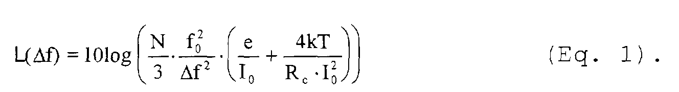
- In this equation, N is the number of delay stages, f0 is the oscillation frequency and Δf is the frequency offset, where the phase noise is measured. As the noise sources, the collector current shot noise and the noise of the load resistor are taken into consideration, while the noise of the base resistance and the 1/f-noise are neglected. From Eq. 1 it is understood, that the tail current I0 and the voltage swing Rc·I0 should be made large, which stands in contradiction to a low power design. A further conclusion from Eq. 1 is, to take only a minimum number of delay stages.
- If we evaluate Eq. 1 with N = 2, I0 = 400µA, Rc = 400Ω, f0 = 6GHz and Δf = 10kHz, we obtain as phase noise L(10kHz) = -41 dBc/Hz. That means for systems with higher order modulation methods like QAM, this oscillator has to be controlled by a wideband PLL with a reference oscillator of respectively low phase noise.
- Therefore, the phase noise performance of the
delay cell oscillator 4 does not satisfy the needs of modern digital transmission systems. When controlled within a PLL, thereference oscillator 6 governs the phase noise of the VCO inside the loop bandwidth. The phase noise So of the PLL-output as a function of the frequency offset Δf may be expressed therefore as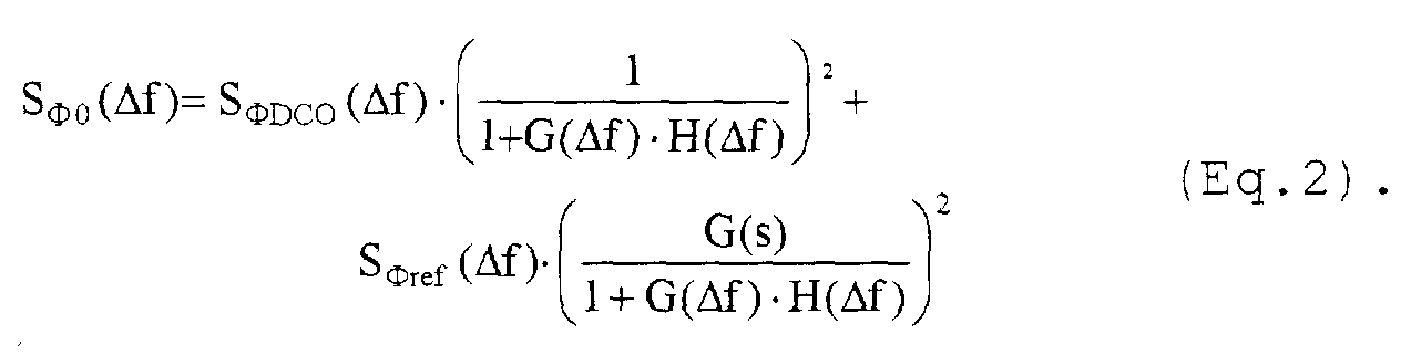
- In Eq. 2, SDCO is the phase noise of the DCO as calculated in accordance with Eq. 1, Sref is the phase noise of the
reference oscillator 6, G(Δf) is the forward loop gain and H(Δf) stands for the reverse loop gain. - As the
reference oscillator 6 inhibits atank circuit 7 of resonance frequency f0ref and quality factor Qref, noise figure Fref and output power Pref, its phase noise Sref may be expressed according to Leesons formula as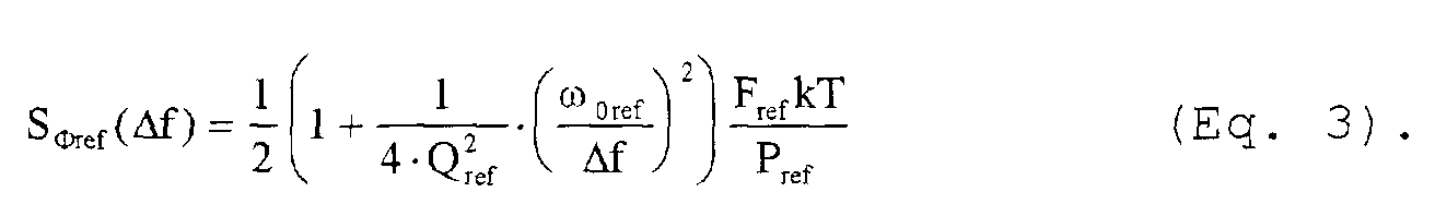
- The forward loop gain G(Δf) depends according
loop filter 3 and on the tuning constant KVCO of theVCO 4. - The reverse loop gain H(Δf) may be expressed as
- Inserting Eq. 4 to Eq. 6 in Eq. 3, the phase noise of the PLL circuit 1-5 can be calculated. For a realistic embodiment, the calculation is based on the assumptions:
- 6. DCO phase noise as calculated in section 3.1 for fDCO = 6 GHz
- 7. DCO tuning constant KDCO = 1000 2π MHz/V
- 8. Phase detector constant KΦ = 0.5 mA/(2π rad)
- 9. Divider factor N = 4
- 10. Loop filter ZL with C1 = 0, C2 = 22 pF, R2 = 15 kΩ
- 11. Reference oscillator Qref = 20, f0ref = 1.5 GHz, Fref = 3, Pref = 0.2 mW
-
- As a result, the PLL is able to improve the phase noise, at e.g. 10 kHz offset frequency, from -41 dBc/Hz (free running VCO) to -78 dBc/Hz (VCO is PLL controlled). However, towards lower frequencies the phase noise increases, as the phase noise of the
reference oscillator 6 increases. The choice of theloop filter 3 is critical, in that it influences the resonance at the characteristic frequency of the PLL. To achieve a good phase noise performance, the low-noise-reference oscillator 6 has to operate also on a high-Q-resonator with Qref > 20 and the bandwidth of the loop PLL should be > 20 MHz. - According to measurements, the DCO frequency may be tuned from 3.5 GHz up to 6 GHz. The phase noise performance is limited by the
reference oscillator 6. Using an external reference with L(10kHz)=-104 dBc/Hz at 1.25 GHz operating frequency, the measured phase noise is -90 dBc/Hz at 5 GHz overall. This is 2 dB worse than the expected theoretical 12 dB reduction in phase noise between reference and DCO. - The high frequency oscillator may comprise also a second loop with a
phase detector 21 coupled to the I/Q output signals of thering oscillator 4, as shown in Fig. 4. Thephase detector 21 provides an error signal Vphase for thering oscillator 4, when the phase difference between the I and the Q signal differs from 90°, so that always orthogonality between the I and Q signals is maintained over the complete frequency bandwidth during the operation of the high frequency oscillator. - The phase control signal Vphase is coupled to the delay cell amplifiers A1 and A2 of the
ring oscillator 4, as shown in Fig. 5. The delay cell amplifiers A1 and A2 are coupled in series, and provide each a phase shift of 90°. The outputs of the delay cells A1, A2 are ground-free, and the output of the delay cell A2 is used for the I+ and the I- signal, and the output of the delay cell A1 is used for the Q+ and the Q- signal, see also Fig. 3. The output of the delay cell A2 is coupled via an inversion IV to the input of the delay cell A1, so that the oscillation condition of 360° is fulfilled. - The
ring oscillator 4 comprises further an amplifier section 2I0 for providing a current of 2I0 to each of the delay cells A1 and A2, and to which amplifier section the control signal Vcont of thecharge pump 2 is coupled, for providing the frequency control. The amplifier sections 2I0 are identical, so that the delay cells A1 and A2 are tuned symmetrically. The amplifier sections 2I0 are coupled to samecurrent source 23. - The control signal of the
phase detector 21 is coupled to a controllablecurrent source 22, which is coupled to each of the amplifier sections 2I0. Via thecurrent source 22 the control voltage Vphase provides an unsymmetry of the curents of thecurrent source 23, via which a discrepancy of the required phase difference of 90° of the I/Q signals is corrected. - A detailed circuit diagram of the
delay cell oscillator 4 is shown in Fig. 6. Thering oscillator 4 consists essentially of the delay cell amplifiers A1 and A2, the feedback loop with the inversion IV, and the control amplifier Ac for phase and frequency control. Thedelay cell amplifier 1 comprises anamplifier 31 which is coupled to the inputs ofamplifier 32 of the delay cell amplifier A2, and which outputs provide the output signals I+/I- and Q+/Q- via load resistors Rc, which are coupled to a supply voltage VCC. - To the outputs of the
amplifier 31 twoamplifiers amplifier 31. The delay cell amplifier A2 is set up withamplifiers - The outputs of the
amplifier 37 are coupled to the inputs of theamplifiers amplifiers amplifier 37 of the control amplifier Ac, to which inputs the control signal Vcont is applied, and which outputs are coupled each as a supply voltage to theamplifiers amplifiers amplifiers amplifier 38 for the delay cell A2, to which input the control signal Vcont is also applied, for a symmetric tuning of the delay cells A1 and A2. - The control amplifier Ac comprises further an
amplifier 39, to which the phase control signal Vphase is applied at the input side. The outputs of theamplifier 39 are each coupled toamplifiers amplifier 37 with respect toamplifier 38, to obtain the correct phase difference of 90° for the output signals I and Q. Thedelay cell oscillator 4 comprises therefore twosymmetrical amplifier sections amplifier 39, which provides the phase control and which is coupled to these amplifier sections.
Claims (9)
- High frequency oscillator comprising a reference oscillator (6) and a phase locked-loop circuit with a phase-frequency detector (1), a charge pump (2), a ring oscillator (4) and a divider (5), the reference oscillator (6) being coupled to the phase-frequency detector (1) for frequency control, characterized in that the ring oscillator (4) is a symmetrical delay cell oscillator containing two delay cell amplifiers (A1, A2).
- High frequency oscillator according to claim 1, characterized in that the reference oscillator (6) is a Colpitts type oscillator with a tank circuit (7), the reference oscillator (6) and the phase locked-loop circuit being integrated within an integrated circuit and the tank circuit (7) being external to the integrated circuit.
- High frequency oscillator according to claim 1 or 2, characterized in that the tuning range of the reference oscillator (6) is 1,25 - 1,5 GHz, and the dividing factor of the divider (5) is four for providing a tuned output range of 5-6 GHz.
- High frequency oscillator according to one of the preceding claims, characterized in that the two delay cell amplifiers (A1, A2) comprise a dual output stage for providing ground-free I/Q output signal generation.
- High frequency oscillator according to one of the preceding claims, characterized in that the charge pump (2) comprises a ground-free loop filter (3), the loop filter (3) being external to the integrated circuit.
- High frequency oscillator according to claim 5, characterized in that the input stage of the charge pump (2) is a differential amplifier and comprises only npn-transistors (11) in the signal path.
- High frequency oscillator according to claim 6, characterized in that the charge pump (2) comprises a first current source with two pnp-transistors (12) and a second, common current source (2I0), both being coupled to the differential amplifier (11), and that the current of first current source (12) is controlled by a reference voltage (VREF) to provide in each of the pnp-transistors half of the current of the second current source (2I0).
- High frequency oscillator according to one of the preceding claims, characterized in that to the delay cell oscillator (4) a loop (loop II) with a phase detector (21) is coupled for a phase control between the I- and the Q-signal.
- High frequency oscillator according to one of the preceding claims, characterized in that the delay cell oscillator (4) comprises two symmetrical amplifier sections (33, 34, 37; 35, 36, 38) for frequency control, which are each coupled to an output of an delay cell amplifier (31, 32), and an amplifier (39) for a phase control, which is coupled to the two amplifier sections (33, 34, 37; 35, 36, 38).
Priority Applications (1)
| Application Number | Priority Date | Filing Date | Title |
|---|---|---|---|
| EP20010114626 EP1175010B1 (en) | 2000-06-28 | 2001-06-19 | High frequency oscillator |
Applications Claiming Priority (3)
| Application Number | Priority Date | Filing Date | Title |
|---|---|---|---|
| EP00113629 | 2000-06-28 | ||
| EP00113629 | 2000-06-28 | ||
| EP20010114626 EP1175010B1 (en) | 2000-06-28 | 2001-06-19 | High frequency oscillator |
Publications (2)
| Publication Number | Publication Date |
|---|---|
| EP1175010A1 true EP1175010A1 (en) | 2002-01-23 |
| EP1175010B1 EP1175010B1 (en) | 2005-11-23 |
Family
ID=26071089
Family Applications (1)
| Application Number | Title | Priority Date | Filing Date |
|---|---|---|---|
| EP20010114626 Expired - Lifetime EP1175010B1 (en) | 2000-06-28 | 2001-06-19 | High frequency oscillator |
Country Status (1)
| Country | Link |
|---|---|
| EP (1) | EP1175010B1 (en) |
Families Citing this family (1)
| Publication number | Priority date | Publication date | Assignee | Title |
|---|---|---|---|---|
| ATE311039T1 (en) * | 2000-06-28 | 2005-12-15 | Thomson Licensing | HIGH FREQUENCY OSCILLATOR |
Citations (2)
| Publication number | Priority date | Publication date | Assignee | Title |
|---|---|---|---|---|
| US5889437A (en) * | 1997-07-10 | 1999-03-30 | Lg Semicon Co., Ltd. | Frequency synthesizer with low jitter noise |
| US6081164A (en) * | 1997-01-09 | 2000-06-27 | Seiko Epson Corporation | PLL oscillator package and production method thereof |
-
2001
- 2001-06-19 EP EP20010114626 patent/EP1175010B1/en not_active Expired - Lifetime
Patent Citations (2)
| Publication number | Priority date | Publication date | Assignee | Title |
|---|---|---|---|---|
| US6081164A (en) * | 1997-01-09 | 2000-06-27 | Seiko Epson Corporation | PLL oscillator package and production method thereof |
| US5889437A (en) * | 1997-07-10 | 1999-03-30 | Lg Semicon Co., Ltd. | Frequency synthesizer with low jitter noise |
Non-Patent Citations (1)
| Title |
|---|
| MEHMET SOYUER ET AL: "A FULLY MONOLITHIC 1.25GHZ CMOS FREQUENCY SYNTHESIZER", SYMPOSIUM ON VLSI CIRCUITS. DIGEST OF TECHNICAL PAPERS. HONOLULU, JUNE 9 - 11, 1994, NEW YORK, IEEE, US, 9 June 1994 (1994-06-09), pages 127 - 128, XP000501055, ISBN: 0-7803-1919-2 * |
Also Published As
| Publication number | Publication date |
|---|---|
| EP1175010B1 (en) | 2005-11-23 |
Similar Documents
| Publication | Publication Date | Title |
|---|---|---|
| US6549082B2 (en) | High frequency oscillator | |
| US7268630B2 (en) | Phase-locked loop using continuously auto-tuned inductor-capacitor voltage controlled oscillator | |
| US7075377B2 (en) | Quadrature voltage controlled oscillators with phase shift detector | |
| US7102454B2 (en) | Highly-linear signal-modulated voltage controlled oscillator | |
| US6833769B2 (en) | Voltage controlled capacitive elements having a biasing network | |
| CA2534370C (en) | Tunable frequency, low phase noise and low thermal drift oscillator | |
| WO2001026230A1 (en) | Pll loop filter with switched-capacitor resistor | |
| US6748041B1 (en) | GM cell based control loops | |
| US7386085B2 (en) | Method and apparatus for high speed signal recovery | |
| US20090096494A1 (en) | Circuit Arrangement For Generating A Complex Signal And The Use Of This Circuit Arrangement In A High-Frequency Transmitter Or Receiver | |
| US20040066220A1 (en) | High-speed high-current programmable charge-pump circuit | |
| JP2005500780A (en) | Tunable quadrature phase shifter | |
| EP1175010B1 (en) | High frequency oscillator | |
| He et al. | A Ka-band dual co-tuning frequency synthesizer with 21.9% locking range and sub-200 fs RMS jitter in CMOS for 5G mm-wave applications | |
| KR100722023B1 (en) | Multifrequency low-power oscillator for telecommunication ic's | |
| Herzel et al. | A 2.5-GHz eight-phase VCO in SiGe BiCMOS technology | |
| JP2001230668A (en) | Phase comparator circuit and pll circuit | |
| JP3492964B2 (en) | Phase shifter and demodulator using the same | |
| Ussmuller et al. | Highly integrated fractional-N synthesizer for locatable wireless sensor nodes | |
| Song et al. | A Sub-$100\\mu\mathrm {W} $ RF Transmitter with 41% Global Efficiency Using Third-Harmonic Edge-Combining Technique and Class-E PA for Low-Power Biomedical Applications | |
| Luo et al. | A 24GHz multi-phase PLL for optical communication | |
| JP3490651B2 (en) | Phase shifter and demodulator using the same | |
| Singh et al. | A Differential output delay cell based ring VCO for improved jitter performance | |
| Lee et al. | 52-GHz Millimetre-Wave PLL Synthesizer | |
| Chen | A 10 Gb/s CMOS half-rate clock and data recovery circuit with direct bang-bang tuning |
Legal Events
| Date | Code | Title | Description |
|---|---|---|---|
| PUAI | Public reference made under article 153(3) epc to a published international application that has entered the european phase |
Free format text: ORIGINAL CODE: 0009012 |
|
| AK | Designated contracting states |
Kind code of ref document: A1 Designated state(s): AT BE CH CY DE DK ES FI FR GB GR IE IT LI LU MC NL PT SE TR |
|
| AX | Request for extension of the european patent |
Free format text: AL;LT;LV;MK;RO;SI |
|
| 17P | Request for examination filed |
Effective date: 20020605 |
|
| AKX | Designation fees paid |
Free format text: AT BE CH CY DE DK ES FI FR GB GR IE IT LI LU MC NL PT SE TR |
|
| 17Q | First examination report despatched |
Effective date: 20040504 |
|
| GRAP | Despatch of communication of intention to grant a patent |
Free format text: ORIGINAL CODE: EPIDOSNIGR1 |
|
| GRAS | Grant fee paid |
Free format text: ORIGINAL CODE: EPIDOSNIGR3 |
|
| RAP1 | Party data changed (applicant data changed or rights of an application transferred) |
Owner name: THOMSON LICENSING |
|
| GRAA | (expected) grant |
Free format text: ORIGINAL CODE: 0009210 |
|
| AK | Designated contracting states |
Kind code of ref document: B1 Designated state(s): AT BE CH CY DE DK ES FI FR GB GR IE IT LI LU MC NL PT SE TR |
|
| PG25 | Lapsed in a contracting state [announced via postgrant information from national office to epo] |
Ref country code: NL Free format text: LAPSE BECAUSE OF FAILURE TO SUBMIT A TRANSLATION OF THE DESCRIPTION OR TO PAY THE FEE WITHIN THE PRESCRIBED TIME-LIMIT Effective date: 20051123 Ref country code: LI Free format text: LAPSE BECAUSE OF FAILURE TO SUBMIT A TRANSLATION OF THE DESCRIPTION OR TO PAY THE FEE WITHIN THE PRESCRIBED TIME-LIMIT Effective date: 20051123 Ref country code: BE Free format text: LAPSE BECAUSE OF FAILURE TO SUBMIT A TRANSLATION OF THE DESCRIPTION OR TO PAY THE FEE WITHIN THE PRESCRIBED TIME-LIMIT Effective date: 20051123 Ref country code: AT Free format text: LAPSE BECAUSE OF FAILURE TO SUBMIT A TRANSLATION OF THE DESCRIPTION OR TO PAY THE FEE WITHIN THE PRESCRIBED TIME-LIMIT Effective date: 20051123 Ref country code: CH Free format text: LAPSE BECAUSE OF FAILURE TO SUBMIT A TRANSLATION OF THE DESCRIPTION OR TO PAY THE FEE WITHIN THE PRESCRIBED TIME-LIMIT Effective date: 20051123 Ref country code: FI Free format text: LAPSE BECAUSE OF FAILURE TO SUBMIT A TRANSLATION OF THE DESCRIPTION OR TO PAY THE FEE WITHIN THE PRESCRIBED TIME-LIMIT Effective date: 20051123 |
|
| REG | Reference to a national code |
Ref country code: GB Ref legal event code: FG4D |
|
| REG | Reference to a national code |
Ref country code: CH Ref legal event code: EP |
|
| REF | Corresponds to: |
Ref document number: 60115158 Country of ref document: DE Date of ref document: 20051229 Kind code of ref document: P |
|
| REG | Reference to a national code |
Ref country code: IE Ref legal event code: FG4D |
|
| REG | Reference to a national code |
Ref country code: GB Ref legal event code: 746 Effective date: 20051221 |
|
| PG25 | Lapsed in a contracting state [announced via postgrant information from national office to epo] |
Ref country code: DK Free format text: LAPSE BECAUSE OF FAILURE TO SUBMIT A TRANSLATION OF THE DESCRIPTION OR TO PAY THE FEE WITHIN THE PRESCRIBED TIME-LIMIT Effective date: 20060223 Ref country code: GR Free format text: LAPSE BECAUSE OF FAILURE TO SUBMIT A TRANSLATION OF THE DESCRIPTION OR TO PAY THE FEE WITHIN THE PRESCRIBED TIME-LIMIT Effective date: 20060223 Ref country code: SE Free format text: LAPSE BECAUSE OF FAILURE TO SUBMIT A TRANSLATION OF THE DESCRIPTION OR TO PAY THE FEE WITHIN THE PRESCRIBED TIME-LIMIT Effective date: 20060223 |
|
| PG25 | Lapsed in a contracting state [announced via postgrant information from national office to epo] |
Ref country code: ES Free format text: LAPSE BECAUSE OF FAILURE TO SUBMIT A TRANSLATION OF THE DESCRIPTION OR TO PAY THE FEE WITHIN THE PRESCRIBED TIME-LIMIT Effective date: 20060306 |
|
| PG25 | Lapsed in a contracting state [announced via postgrant information from national office to epo] |
Ref country code: PT Free format text: LAPSE BECAUSE OF FAILURE TO SUBMIT A TRANSLATION OF THE DESCRIPTION OR TO PAY THE FEE WITHIN THE PRESCRIBED TIME-LIMIT Effective date: 20060424 |
|
| NLV1 | Nl: lapsed or annulled due to failure to fulfill the requirements of art. 29p and 29m of the patents act | ||
| REG | Reference to a national code |
Ref country code: CH Ref legal event code: PL |
|
| PG25 | Lapsed in a contracting state [announced via postgrant information from national office to epo] |
Ref country code: IE Free format text: LAPSE BECAUSE OF NON-PAYMENT OF DUE FEES Effective date: 20060619 |
|
| PG25 | Lapsed in a contracting state [announced via postgrant information from national office to epo] |
Ref country code: MC Free format text: LAPSE BECAUSE OF NON-PAYMENT OF DUE FEES Effective date: 20060630 |
|
| ET | Fr: translation filed | ||
| PLBE | No opposition filed within time limit |
Free format text: ORIGINAL CODE: 0009261 |
|
| STAA | Information on the status of an ep patent application or granted ep patent |
Free format text: STATUS: NO OPPOSITION FILED WITHIN TIME LIMIT |
|
| 26N | No opposition filed |
Effective date: 20060824 |
|
| REG | Reference to a national code |
Ref country code: IE Ref legal event code: MM4A |
|
| PG25 | Lapsed in a contracting state [announced via postgrant information from national office to epo] |
Ref country code: TR Free format text: LAPSE BECAUSE OF FAILURE TO SUBMIT A TRANSLATION OF THE DESCRIPTION OR TO PAY THE FEE WITHIN THE PRESCRIBED TIME-LIMIT Effective date: 20051123 Ref country code: LU Free format text: LAPSE BECAUSE OF NON-PAYMENT OF DUE FEES Effective date: 20060619 |
|
| PG25 | Lapsed in a contracting state [announced via postgrant information from national office to epo] |
Ref country code: CY Free format text: LAPSE BECAUSE OF FAILURE TO SUBMIT A TRANSLATION OF THE DESCRIPTION OR TO PAY THE FEE WITHIN THE PRESCRIBED TIME-LIMIT Effective date: 20051123 |
|
| REG | Reference to a national code |
Ref country code: FR Ref legal event code: PLFP Year of fee payment: 16 |
|
| REG | Reference to a national code |
Ref country code: FR Ref legal event code: PLFP Year of fee payment: 17 |
|
| REG | Reference to a national code |
Ref country code: DE Ref legal event code: R082 Ref document number: 60115158 Country of ref document: DE Representative=s name: HOFSTETTER, SCHURACK & PARTNER PATENT- UND REC, DE |
|
| REG | Reference to a national code |
Ref country code: FR Ref legal event code: PLFP Year of fee payment: 18 |
|
| PGFP | Annual fee paid to national office [announced via postgrant information from national office to epo] |
Ref country code: DE Payment date: 20180622 Year of fee payment: 18 |
|
| PGFP | Annual fee paid to national office [announced via postgrant information from national office to epo] |
Ref country code: FR Payment date: 20180620 Year of fee payment: 18 |
|
| PGFP | Annual fee paid to national office [announced via postgrant information from national office to epo] |
Ref country code: IT Payment date: 20180625 Year of fee payment: 18 Ref country code: GB Payment date: 20180627 Year of fee payment: 18 |
|
| REG | Reference to a national code |
Ref country code: DE Ref legal event code: R119 Ref document number: 60115158 Country of ref document: DE |
|
| GBPC | Gb: european patent ceased through non-payment of renewal fee |
Effective date: 20190619 |
|
| PG25 | Lapsed in a contracting state [announced via postgrant information from national office to epo] |
Ref country code: IT Free format text: LAPSE BECAUSE OF NON-PAYMENT OF DUE FEES Effective date: 20190619 Ref country code: GB Free format text: LAPSE BECAUSE OF NON-PAYMENT OF DUE FEES Effective date: 20190619 Ref country code: DE Free format text: LAPSE BECAUSE OF NON-PAYMENT OF DUE FEES Effective date: 20200101 |
|
| PG25 | Lapsed in a contracting state [announced via postgrant information from national office to epo] |
Ref country code: FR Free format text: LAPSE BECAUSE OF NON-PAYMENT OF DUE FEES Effective date: 20190630 |