EP1174943A1 - Dual mode band-pass filter - Google Patents
Dual mode band-pass filter Download PDFInfo
- Publication number
- EP1174943A1 EP1174943A1 EP01110467A EP01110467A EP1174943A1 EP 1174943 A1 EP1174943 A1 EP 1174943A1 EP 01110467 A EP01110467 A EP 01110467A EP 01110467 A EP01110467 A EP 01110467A EP 1174943 A1 EP1174943 A1 EP 1174943A1
- Authority
- EP
- European Patent Office
- Prior art keywords
- metal film
- band
- pass filter
- dielectric body
- resonance
- Prior art date
- Legal status (The legal status is an assumption and is not a legal conclusion. Google has not performed a legal analysis and makes no representation as to the accuracy of the status listed.)
- Granted
Links
- 230000009977 dual effect Effects 0.000 title 1
- 239000002184 metal Substances 0.000 claims abstract description 76
- 229910052751 metal Inorganic materials 0.000 claims abstract description 76
- 230000008878 coupling Effects 0.000 claims abstract description 29
- 238000010168 coupling process Methods 0.000 claims abstract description 29
- 238000005859 coupling reaction Methods 0.000 claims abstract description 29
- 230000005684 electric field Effects 0.000 claims abstract description 25
- 230000000644 propagated effect Effects 0.000 claims description 7
- 230000002093 peripheral effect Effects 0.000 claims description 4
- 230000004048 modification Effects 0.000 description 15
- 238000012986 modification Methods 0.000 description 15
- 230000005540 biological transmission Effects 0.000 description 10
- QNRATNLHPGXHMA-XZHTYLCXSA-N (r)-(6-ethoxyquinolin-4-yl)-[(2s,4s,5r)-5-ethyl-1-azabicyclo[2.2.2]octan-2-yl]methanol;hydrochloride Chemical compound Cl.C([C@H]([C@H](C1)CC)C2)CN1[C@@H]2[C@H](O)C1=CC=NC2=CC=C(OCC)C=C21 QNRATNLHPGXHMA-XZHTYLCXSA-N 0.000 description 8
- 238000009826 distribution Methods 0.000 description 6
- 230000015572 biosynthetic process Effects 0.000 description 4
- 239000003990 capacitor Substances 0.000 description 4
- 239000004020 conductor Substances 0.000 description 4
- 239000000463 material Substances 0.000 description 3
- 238000000034 method Methods 0.000 description 3
- 238000004519 manufacturing process Methods 0.000 description 2
- 239000007769 metal material Substances 0.000 description 2
- 239000011224 oxide ceramic Substances 0.000 description 2
- 229910052574 oxide ceramic Inorganic materials 0.000 description 2
- 238000000059 patterning Methods 0.000 description 2
- 230000008569 process Effects 0.000 description 2
- 239000000758 substrate Substances 0.000 description 2
- 229920003002 synthetic resin Polymers 0.000 description 2
- 239000000057 synthetic resin Substances 0.000 description 2
- 239000000919 ceramic Substances 0.000 description 1
- 230000008859 change Effects 0.000 description 1
- 238000004891 communication Methods 0.000 description 1
- 230000003247 decreasing effect Effects 0.000 description 1
- 238000010586 diagram Methods 0.000 description 1
- 230000000694 effects Effects 0.000 description 1
- 230000005672 electromagnetic field Effects 0.000 description 1
- 239000003822 epoxy resin Substances 0.000 description 1
- 229920000647 polyepoxide Polymers 0.000 description 1
- 229920005989 resin Polymers 0.000 description 1
- 239000011347 resin Substances 0.000 description 1
Images


Classifications
-
- H—ELECTRICITY
- H01—ELECTRIC ELEMENTS
- H01P—WAVEGUIDES; RESONATORS, LINES, OR OTHER DEVICES OF THE WAVEGUIDE TYPE
- H01P7/00—Resonators of the waveguide type
- H01P7/08—Strip line resonators
-
- H—ELECTRICITY
- H01—ELECTRIC ELEMENTS
- H01P—WAVEGUIDES; RESONATORS, LINES, OR OTHER DEVICES OF THE WAVEGUIDE TYPE
- H01P1/00—Auxiliary devices
- H01P1/20—Frequency-selective devices, e.g. filters
- H01P1/201—Filters for transverse electromagnetic waves
- H01P1/203—Strip line filters
- H01P1/20327—Electromagnetic interstage coupling
- H01P1/20354—Non-comb or non-interdigital filters
- H01P1/20381—Special shape resonators
-
- H—ELECTRICITY
- H01—ELECTRIC ELEMENTS
- H01P—WAVEGUIDES; RESONATORS, LINES, OR OTHER DEVICES OF THE WAVEGUIDE TYPE
- H01P7/00—Resonators of the waveguide type
- H01P7/08—Strip line resonators
- H01P7/082—Microstripline resonators
Definitions
- the present invention relates to a band-pass filter, and more particularly to a band-pass filter for use, for example, in a communication device which operates in a range of from a microwave band to a millimeter wave band, for example.
- FIG. 17 is an equivalent circuit diagram of a conventional LC filter.
- the LC filter includes first and second resonators 101 and 102.
- the first and second resonators 101 and 102 each include a capacitor C and an inductor L, which are connected in parallel to each other.
- a monolithic capacitor and a monolithic inductor are integrated with each other in a single body. That is, two resonators each including a monolithic capacitor portion and a monolithic inductor portion are provided to define a monolithic electronic component such that the circuit arrangement shown in FIG. 17 is produced.
- the two resonators 101 and 102 are coupled to each other via a coupling capacitor Cl.
- preferred embodiments of the present invention provide a band-pass filter of which the application at a higher frequency and the miniaturization are easily realized, and of which the conditions required for control of the dimensional accuracy are facilitated.
- a band-pass filter includes a dielectric body, a metal film provided on the surface of the dielectric body or inside of the dielectric body, a ground electrode provided on the surface of the dielectric body or inside of the dielectric body, and opposed to the metal film via at least a portion of the layers of the dielectric body, and input-output coupling circuits coupled to first and second portions of the outer peripheral edge of the metal film, the shape and size of the metal film and the positions of the coupling points of the input-output coupling circuits being selected such that a first resonance mode of a wave being propagated in a direction that is substantially parallel to the imaginary straight line passing through the coupling points of the input-output coupling circuit, and a second resonance mode of a wave being propagated in the substantially perpendicular direction to the imaginary straight line are generated, the metal film having a protruding portion or a concavity provided thereon in the position where the resonance electric field in at least one of the resonance modes is strong, such that the first and
- the metal film has a substantially rectangular, substantially rhomboid, or substantially triangular shape.
- the metal film has a substantially rectangular planar shape, and the protruding portions or concavities are provided on a pair of sides of the substantially rectangular shape.
- the metal film has a substantially rhombic planar shape, and the protruding portion or the concavity is provided on one end side of one of the diagonal lines of the substantially rhombic shape.
- one metal film is provided on a dielectric body or inside of the dielectric body.
- Input-output coupling circuits are provided in first and second portions in the outer peripheral edge of the metal film.
- the resonance is determined by the shape and size of the metal film and the coupling points of the input-output coupling circuits. This will be described with reference to FIGS. 4 to 6.
- a metal film 3 is provided on the upper surface of a dielectric body 2.
- a ground electrode is provided on the under surface of the dielectric body 2 in opposition to the metal film 3.
- the metal film 3 preferably has a substantially rectangular shape.
- Input-output coupling circuits 5 and 6 are capacitively-coupled to a pair of the short sides 3a and 3b of the metal film 3 via gaps, respectively.
- the input-output coupling circuits 5 and 6 contain input-output capacity forming patterns 5a and 6a provided on the upper surface of the dielectric body 2.
- the input-output capacity forming patterns 5a and 6a are connected to micro-strip lines 5b and 6b as external lines provided on a mounting mother substrate 110 via side-surface electrodes (not shown) provided on the side-surfaces of the dielectric body 2, respectively.
- FIG. 5 shows the frequency characteristic of the resonator 1.
- the solid line in FIG. 5 represents the transmission characteristic of the resonator 1, and the broken line represents the reflection characteristic thereof.
- the resonator 1 has a first resonance point A (hereinafter, the resonance mode at the frequency is referred to as a resonance mode A) at which the resonance frequency is lowest, and a second resonance point B (hereinafter, the resonance mode at the frequency is referred to as a resonance mode B) at which the resonance frequency is the next lowest.
- the above-mentioned resonance modes A and B are not coupled to each other. Accordingly, the resonator does not constitute a band-pass filter.
- FIG. 6 schematically shows the portions of the resonator 1 shown in FIG. 4 in which the resonance electric fields in the resonance mode A are strong. That is, in the portions indicated by arrows A1 and A2, the resonance electric fields are strong. In other words, in the resonance mode A, the resonance electric fields are strong near a pair of the short sides 3a and 3b of the substantially rectangular metal film 3.
- the resonance electric field distribution in the resonance mode B was investigated, though the results are not specifically shown. It was ascertained that the resonance electric fields are strong near a pair of the long sides 3c and 3d of the metal film 3.
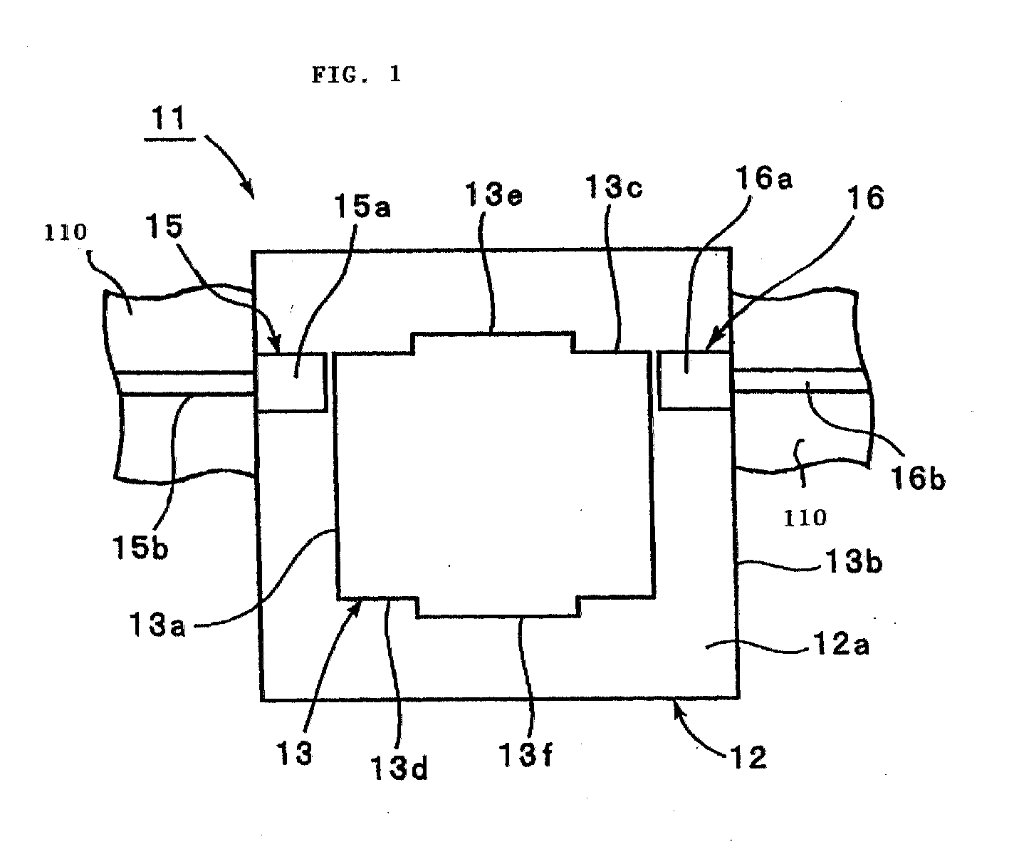
- FIG. 1 is a schematic plan view of a band-pass filter according to a first preferred embodiment of the present invention.
- FIG. 2 is a perspective view of the band-pass filter.
- a metal film 13 is provided on the upper surface 12a of a dielectric body 12, and a ground electrode 14 is provided on the lower surface 12b.
- Materials for forming the dielectric body 12 are not specifically limited.
- appropriate synthetic resins such as fluoro-resin, epoxy resin, or other suitable synthetic resins, oxide ceramics, and so forth may be used.
- the dielectric body 12 is made of oxides of Mg, Si, and Al.
- the metal film 13 and the ground electrode 14 may be made of any appropriate metal material. In this preferred embodiment, they are preferably made of Cu.
- substantially rectangular protruding portions 13e and 13f are arranged to protrude externally from a pair of the long sides 13c and 13d of the metal film 13, as is different from the example shown in FIG. 4.
- the protruding portions 13e and 13f are preferably made of the same material as the metal film 13. That is, in the process of forming the metal film 13, protruding portions 13e and 13f are formed simultaneously with the metal film 13 by patterning or printing or other suitable process.
- Input-output coupling circuits 15 and 16 are provided on the upper surface of the dielectric body 12 with gaps provided between the input-output coupling circuits 15 and 16 and a pair of the short sides 13a and 13b of the metal film 13, respectively.
- the input-output coupling circuits 15 and 16 contain capacity forming patterns 15a and 16a which are provided on the upper surface 12a of the dielectric body 12 with the gaps provided between the capacity forming patterns 15a and 16a and a pair of the short sides 13a and 13b of the metal film 13, respectively.
- the capacity forming patterns 15a and 16a are connected via side-surface electrodes 15c and 16c provided on the side surfaces of the dielectric body 12 (the side-face electrode 16c is not shown) to micro-strip lines 15b and 16b as external lines provided on a dielectric mother substrate 110.
- a voltage is input-output to the metal film 13 via the input-output coupling circuits 15 and 16. That is, a desired signal is transmitted to the metal film 13 via the micro-strip line 15b (or 16b), the side-surface electrodes 15c (or 16c), and the capacity-forming pattern 15a (or 16a).
- the metal film 13 since the metal film 13 has a shape and size similar to that of the metal film 3 (FIG. 4), the first and second resonance modes A and B are generated.
- the second resonance mode B when the second resonance mode B is generated, a portion of the resonance electric field distributions where the resonance electric fields are strong are relaxed, due to the presence of the protruding portions 13e and 13f, such that the resonance frequency in the second resonance mode B is shifted to the low frequency side.
- the first and second resonance modes A and B are coupled to each other, whereby a characteristic required for the band-pass filter is obtained.
- the metal film 13 a metal film made of Cu, having the following approximate sizes is provided.
- the lengths of the short sides 13a and 13b were about 1.3 mm, and the lengths of the long sides 13c and 13d were about 1.5 mm, respectively.
- the protruding portions 13e and 13f the lengths along the long sides 13c and 13d were about 1.0 mm, and the widths perpendicular to the length direction, that is, the protruding lengths were about 0.2 mm, respectively.
- the film thickness was about 4 ⁇ m.
- the capacity forming patterns 15a and 16a were provided with gaps of about 80 ⁇ m being provided between the capacity forming patterns 15a and 16a and the short sides 13a and 13b, and in opposition to the short sides 13a and 13b over the length of about 400 ⁇ m, respectively.
- the ground electrode 14 was provided on substantially the entire of the lower surface of the dielectric body 12.
- FIG. 3 shows the frequency characteristic of the band-pass filter 11.
- solid line C and broken line D show the transmission and reflection characteristics of the band-pass filter 11 of this preferred embodiment, respectively.
- the transmission and reflection characteristics of the resonator 1 of FIG. 6 are shown as represented by thin solid line A and thin broken line B, respectively.
- the resonator 1 of which the characteristics are represented by the solid line A and the broken line B is provided in the same manner as the above example except that the protruding portions 13e and 13f are not provided.
- the first and second resonance modes are coupled, such that a characteristic required for the band-pass filter is obtained.
- the resonance electric field distributions in the second resonance mode are changed, since the protruding portions 13e and 13f are provided in the positions where the resonance electric fields in the second resonance mode are strong.
- the resonance frequency in the second resonance mode is shifted to the low frequency side, and is coupled to the first resonance mode.
- the formation of the protruding portions 13e and 13f causes the resonance frequency in the second resonance mode to change, such that the second resonance mode is coupled to the first resonance mode.
- concavities may be provided instead of the protruding portions, such that the first and second resonance modes are coupled to each other.
- FIG. 7 is a schematic plan view of the band-pass filter of the modification of the first preferred embodiment.
- the concavities 13g and 13h are provided on the sides of the short sides 13a and 13b. Accordingly, the first resonance electric fields are strengthened, due to effects of the concavities 13g and 13h. Therefore, the resonance frequency in the first resonance mode is increased, so that the second and first resonance modes are coupled to each other. That is, the sizes of the concavities 13g and 13h are determined such that the first and second resonance modes are coupled to each other to obtain a characteristic required for the band-pass filter.
- FIG. 8 shows the frequency characteristic of the band-pass filter 18 of this modification.
- Solid line E and broken line F in FIG. 8 represent the transmission and reflection characteristics of the band-pass filter 18 of this modification.
- the transmission and reflection characteristics of the resonator 1 of FIG. 6 are shown by solid line A and broken line B.
- a protruding portion and a concavity may be provided on only one side of a pair of the opposed sides, respectively.
- the substantially rectangular metal film is preferably used.
- the shape and size of the metal film is not specifically limited.
- the metal film may have an optional shape and size such as a rhombus, a triangle, an ellipse, or other suitable shape.
- the metal film preferably has a substantially rhombic planar shape.
- FIG 9 is a schematic plan view of a band-pass filter 21 according to a second preferred embodiment of the present invention.
- a substantially rhombic metal film 23 is used in the band-pass filter 21.
- a protruding portion 23a is provided on one end side of the short diagonal line of the metal film 23.
- the protruding portion 23a extends from a portion of the sides 23b and 23c outward of the rhombus, covering the corner portion sandwiched between the sides 23b and 23c.
- the metal film 23 and the protruding portion 23a are preferably made of the same metal material, and are formed simultaneously, in connection to each other by patterning, printing or other suitable method.
- Input-output capacity forming patterns 25a and 26a are provided near the other end side of the short diagonal line of the metal film 23.
- the input-output capacity forming patterns 25a and 26a have edges 25a 1 and 26a 1 elongating in a direction that is substantially parallel to the sides 23d and 23e, respectively.
- the band-pass filter 21 is configured in the same manner as the band-pass filter 11 of the first preferred embodiment.
- the similar components are designated by the same reference numerals, and the description is omitted.
- the first and second resonance modes are coupled to each other, due to the protruding portion 23a, such that a characteristic required for a band-pass filter is obtained. This will be described with reference to FIGS. 10 to 14.
- FIG. 11 is a schematic plan view of a resonator 22 configured in the same manner as the second preferred embodiment except that the above-described protruding portion is not provided.
- FIG. 12 shows the frequency characteristic of the resonator 22.
- the dielectric body 12 is preferably a body made of a ceramic containing oxides of Mg, Si, and Al as major components similarly to the first preferred embodiment. Materials for forming the input-output capacity forming patterns, the ground electrodes, and the metal film 23 are the same as those for the first preferred embodiment.
- the sizes of the short diagonal lines are preferably, for example, about 2.0 mm, and the sizes of the long diagonal lines are about 2.4 mm, respectively.
- the portions of the input-output capacity forming patterns 25a and 26a, opposed to the sides 25d and 25e, preferably have a length of about 0.4 mm, respectively.
- the widths of the gaps opposed to the sides 23d and 23e are about 80 ⁇ m, respectively.
- FIG. 12 shows the frequency characteristic of the resonator 22.
- Solid line A2 represents the transmission characteristic
- broken line B2 represents the reflection characteristic.
- a first resonance point G hereinafter, the resonance mode at the frequency is referred to as resonance mode G
- a second resonance point H hereinafter, the resonance mode at the frequency is referred to as resonance mode H
- the first and second resonance modes G and H are not coupled to each other.
- the resonance electric field distributions in the first and second resonance modes G and H were investigated.
- the portions G where the resonance electric fields are strong appear on both of the ends of the long diagonal lines of the rhombus metal film 23 as shown in FIG. 13.
- the portions H where strong electric fields are generated appear near to both of the ends of the short diagonal ones as shown in FIG. 14.
- the resonance electric fields of resonance on the side where the protruding portion or the concavity is provided is controlled, and the first and second resonance modes G and H are coupled to each other.
- the protruding portion 23a shown in FIG. 9 is provided on the basis of the above-described information.
- the protruding portion 23a is provided on one end side of the short diagonal lines, and acts in such a manner that the resonance electric field in the resonance mode in which a wave is propagated in the short diagonal line direction, that is, in the second resonance mode H is weakened. Accordingly, the resonance frequency in the second resonance mode H is reduced, such that the first and second resonance modes are coupled to each other.
- the size and width of the protruding portion 23a are decreased such that the protruding portion 23a reduces the resonance frequency of the second resonance mode G and causes the second resonance mode H to be coupled to the first resonance mode G.
- FIG. 10 shows the frequency characteristic of the band-pass filter 21 of the second preferred embodiment.
- solid line I represents the transmission characteristic
- broken line J represents the reflection characteristic.
- solid lines A2 and broken line B2 are shown by solid lines A2 and broken line B2 together with those of the band-pass filter 21.
- the first and second resonance modes generated in the substantially rhombic metal film 23 are coupled to each other, such that a characteristic required for the band-pass filter is obtained.
- Protruding portions may be provided on both of the ends of the short diagonal line.
- the protruding portion 23a is provided on one end side of the short diagonal line of the substantially rhombic metal film 23. Also in the second preferred embodiment, a concavity may be provided instead of the protruding portion.
- FIG. 15 shows such a modification of the second preferred embodiment as described above.
- concavities 23g and 23h are provided on both of the ends of the long diagonal line of the substantially rhombic metal film 23.
- a band-pass filter 25 is produced in the same manner that the second preferred embodiment except that as the concavities 23g and 23h, substantially rectangular concavities each of which the concave portion has a height of about 0.3 mm and a bottom length of about 0.6 mm are provided, and the protruding portion 23a is not provided.
- FIG. 16 shows the frequency characteristic of the band-pass filter 25.
- solid line K represents the transmission characteristic
- broken line L represents the reflection characteristic.
- the frequency characteristic (the frequency characteristic shown in FIG. 12) of the resonator 22 of FIG. 11, having no concavities and protruding portions, is shown together with that of the band-pass filter 25, in FIG. 16.
- the first and second resonance modes are coupled to each other, due to the formation of the concavities 23g and 23h, as seen in FIG. 16, such that a characteristic required for the band-pass filter is obtained.
- One of the concavities 23g and 23h may be provided alone, also.
- the metal film is provided on the dielectric body, and the ground electrode is provided on the lower surface.
- the metal film may be provided inside of the dielectric body.
- the ground electrode may be provided inside of the dielectric body.
- the formation positions of the metal film and the ground electrode are not specifically limited, provided that the metal film and the ground electrode are opposed to each other via at least a portion of the layers of the dielectric body.
- the metal film and the input-output circuits are capacity-coupled to each other via a gap between them.
- strip lines or micro-strip lines as the input-output circuits may be connected directly to the metal film.
- the band-pass filter of preferred embodiments of the present invention may have an appropriate configuration such as a tri-plate configuration.
- external lines and the input-output circuits may be connected to each other via side surface electrodes provided on the side surfaces of the dielectric body. Moreover, they may be connected through a via-hole electrode provided inside of the dielectric body.
- the first and second resonance modes can be coupled to each other simply by selecting the shape and size of one metal film and the coupling positions of the input-output coupling circuits, and forming the protuberant portion or concavity in the metal film.
- a band-pass filter having a pass-band in a desired frequency band is provided. Accordingly, the configuration of the band-pass filter which can be operated in a high frequency band can be simplified. Furthermore, when the band-pass filter is produced, the dimensional accuracy can be easily controlled.
- a band-pass filter usable in a high frequency band can be provided inexpensively and easily.
- the shape and size of the metal film is not specifically limited, and may have an optional shape such as a rectangle, a rhombus, a triangle, or other suitable shape.
- band-pass filters having various shapes of metal films can be formed.
- the input-output coupling circuits is provided on the side of a pair of the sides different from the above sides of the rectangle.
- the band-pass filter is easily miniaturized.
- the input-output coupling circuits is provided on one end side of the diagonal line which is opposite to the other end side where the protruding portion or concavity is provided.
Abstract
Description
- The present invention relates to a band-pass filter, and more particularly to a band-pass filter for use, for example, in a communication device which operates in a range of from a microwave band to a millimeter wave band, for example.
- Conventionally, LC filters have been widely used as band-pass filters. FIG. 17 is an equivalent circuit diagram of a conventional LC filter.
- The LC filter includes first and
second resonators second resonators resonators - When an LC filter having the circuit configuration shown in FIG. 17 is formed as a single component, many conductor patterns and via-hole electrodes for connecting the conductor patterns must be provided. Accordingly, these conductor patterns and via-hole electrodes must be very accurately formed.
- Moreover, since many electronic component elements must be formed as described above, the structure of the LC filter is complicated, and miniaturization thereof is not possible.
- Furthermore, in general, the resonance frequency f of an LC filter is expressed as f = 1/2 π (LC)1/2, in which L represents the inductance of a resonator, and C represents the capacitance thereof. Accordingly, when a relatively high frequency LC filter is produced, the product of the capacitance C and the inductance L of the resonator must be reduced. That is, for production of a high frequency LC filter, it is necessary to reduce production errors of the resonator with respect to the inductance L and the capacitance C. Thus, for development of a higher frequency LC filter, the accuracies of many conductor patterns and via-holes must be enhanced. Thus, the development of conventional high frequency LC filters is very limited.
- To overcome the above-described problems with the prior art, preferred embodiments of the present invention provide a band-pass filter of which the application at a higher frequency and the miniaturization are easily realized, and of which the conditions required for control of the dimensional accuracy are facilitated.
- According to preferred embodiment of the present invention, a band-pass filter includes a dielectric body, a metal film provided on the surface of the dielectric body or inside of the dielectric body, a ground electrode provided on the surface of the dielectric body or inside of the dielectric body, and opposed to the metal film via at least a portion of the layers of the dielectric body, and input-output coupling circuits coupled to first and second portions of the outer peripheral edge of the metal film, the shape and size of the metal film and the positions of the coupling points of the input-output coupling circuits being selected such that a first resonance mode of a wave being propagated in a direction that is substantially parallel to the imaginary straight line passing through the coupling points of the input-output coupling circuit, and a second resonance mode of a wave being propagated in the substantially perpendicular direction to the imaginary straight line are generated, the metal film having a protruding portion or a concavity provided thereon in the position where the resonance electric field in at least one of the resonance modes is strong, such that the first and second resonance modes are coupled to each other.
- Preferably, the metal film has a substantially rectangular, substantially rhomboid, or substantially triangular shape.
- Also preferably, the metal film has a substantially rectangular planar shape, and the protruding portions or concavities are provided on a pair of sides of the substantially rectangular shape.
- Moreover, preferably, the metal film has a substantially rhombic planar shape, and the protruding portion or the concavity is provided on one end side of one of the diagonal lines of the substantially rhombic shape.
- The features, characteristics, elements and advantages of the present invention will be clear from the following detailed description of preferred embodiments of the invention in conjunction with the accompanying drawings.
-
- FIG. 1 is a schematic plan view of a band-pass filter according to a first preferred embodiment of the present invention.
- FIG. 2 is a perspective view of the band-pass filter of the first preferred embodiment.
- FIG. 3 is a graph showing the frequency characteristics of the first preferred embodiment and a resonator prepared for comparison thereto.
- FIG. 4 is a schematic plan view of the resonator prepared for the comparison to preferred embodiments of the present invention.
- FIG. 5 is a graph showing the frequency characteristic of the resonator shown in FIG. 4.
- FIG. 6 is a schematic plan view illustrating the portions of the resonator shown in FIG. 4 in which strong resonance electric fields are generated at second resonation.
- FIG. 7 is a schematic plan view of a band-pass filter as a modification of the first preferred embodiment.
- FIG. 8 is a graph showing the frequency characteristics of the band-pass filter as the modification shown in FIG. 7 and a resonator prepared for comparison.
- FIG. 9 is a schematic plan view of a band-pass filter according to a second preferred embodiment of the present invention.
- FIG. 10 is a graph showing the frequency characteristics of the band-pass filter of the second preferred embodiment and a resonator prepared for comparison.
- FIG. 11 is a schematic plan view of the resonator prepared for comparison with the second preferred embodiment.
- FIG. 12 is a graph showing the frequency characteristic of the resonator shown in FIG. 11.
- FIG. 13 is a schematic plan view illustrating the portions of the resonator shown in FIG. 11 in which strong resonance electric fields are generated at the first resonation.
- FIG. 14 is a schematic plan view illustrating the portions of the resonator shown in FIG. 11 in which strong resonance electric fields are generated at the second resonation.
- FIG. 15 is a schematic plan view of a band-pass filter according to a modification of the second preferred embodiment.
- FIG. 16 is a graph showing the frequency characteristics of the band-pass filter as the modification shown in FIG. 15 and the resonator shown in FIG. 11.
- FIG. 17 illustrates the circuit configuration of a conventional LC filter.
-
- Hereinafter, preferred embodiments of a band-pass filter of the present invention will be described with reference to the drawings.
- In the band-pass filter of various preferred embodiments of the present invention, one metal film is provided on a dielectric body or inside of the dielectric body. Input-output coupling circuits are provided in first and second portions in the outer peripheral edge of the metal film. In a resonator having the above-described configuration, the resonance is determined by the shape and size of the metal film and the coupling points of the input-output coupling circuits. This will be described with reference to FIGS. 4 to 6.
- As a resonator having the above-described configuration, the inventors of this application have prepared a resonator having a micro-strip configuration shown in FIG. 4. In a
resonator 1 shown in FIG. 4, ametal film 3 is provided on the upper surface of adielectric body 2. A ground electrode is provided on the under surface of thedielectric body 2 in opposition to themetal film 3. Themetal film 3 preferably has a substantially rectangular shape. Input-output coupling circuits short sides metal film 3 via gaps, respectively. The input-output coupling circuits capacity forming patterns 5a and 6a provided on the upper surface of thedielectric body 2. The input-outputcapacity forming patterns 5a and 6a are connected tomicro-strip lines mounting mother substrate 110 via side-surface electrodes (not shown) provided on the side-surfaces of thedielectric body 2, respectively. - FIG. 5 shows the frequency characteristic of the
resonator 1. The solid line in FIG. 5 represents the transmission characteristic of theresonator 1, and the broken line represents the reflection characteristic thereof. - As seen in the transmission characteristic shown in FIG. 5, the
resonator 1 has a first resonance point A (hereinafter, the resonance mode at the frequency is referred to as a resonance mode A) at which the resonance frequency is lowest, and a second resonance point B (hereinafter, the resonance mode at the frequency is referred to as a resonance mode B) at which the resonance frequency is the next lowest. The above-mentioned resonance modes A and B are not coupled to each other. Accordingly, the resonator does not constitute a band-pass filter. - FIG. 6 schematically shows the portions of the
resonator 1 shown in FIG. 4 in which the resonance electric fields in the resonance mode A are strong. That is, in the portions indicated by arrows A1 and A2, the resonance electric fields are strong. In other words, in the resonance mode A, the resonance electric fields are strong near a pair of theshort sides rectangular metal film 3. - Furthermore, the resonance electric field distribution in the resonance mode B was investigated, though the results are not specifically shown. It was ascertained that the resonance electric fields are strong near a pair of the
long sides metal film 3. - The resonance electric field distributions, described or shown in this specification and the drawings are results obtained using of an electromagnetic field simulator HFSS produced by Hewlett-Packard Inc.
- Based on the fact that the portions of the metal film where the resonance electric fields are strong in the resonance modes A and B are different from each other as described above, the inventors of this application assumed that the resonance modes A and B could be coupled to each other by control of the resonance electric field distributions in the resonance modes A and B, and thereby, a band-pass filter would be realized. On this assumption, the present invention has been devised.
- FIG. 1 is a schematic plan view of a band-pass filter according to a first preferred embodiment of the present invention. FIG. 2 is a perspective view of the band-pass filter.
- In a band-
pass filter 11, ametal film 13 is provided on theupper surface 12a of adielectric body 12, and aground electrode 14 is provided on the lower surface 12b. Materials for forming thedielectric body 12 are not specifically limited. For example, appropriate synthetic resins such as fluoro-resin, epoxy resin, or other suitable synthetic resins, oxide ceramics, and so forth may be used. In this preferred embodiment, thedielectric body 12 is made of oxides of Mg, Si, and Al. - The
metal film 13 and theground electrode 14 may be made of any appropriate metal material. In this preferred embodiment, they are preferably made of Cu. - Moreover, in the
metal film 13, substantially rectangular protrudingportions long sides metal film 13, as is different from the example shown in FIG. 4. - The protruding
portions metal film 13. That is, in the process of forming themetal film 13, protrudingportions metal film 13 by patterning or printing or other suitable process. - Input-
output coupling circuits dielectric body 12 with gaps provided between the input-output coupling circuits short sides metal film 13, respectively. The input-output coupling circuits capacity forming patterns 15a and 16a which are provided on theupper surface 12a of thedielectric body 12 with the gaps provided between thecapacity forming patterns 15a and 16a and a pair of theshort sides metal film 13, respectively. Thecapacity forming patterns 15a and 16a are connected via side-surface electrodes 15c and 16c provided on the side surfaces of the dielectric body 12 (the side-face electrode 16c is not shown) tomicro-strip lines dielectric mother substrate 110. - In the band-
pass filter 11 of this preferred embodiment, a voltage is input-output to themetal film 13 via the input-output coupling circuits metal film 13 via themicro-strip line 15b (or 16b), the side-surface electrodes 15c (or 16c), and the capacity-formingpattern 15a (or 16a). In this case, since themetal film 13 has a shape and size similar to that of the metal film 3 (FIG. 4), the first and second resonance modes A and B are generated. However, when the second resonance mode B is generated, a portion of the resonance electric field distributions where the resonance electric fields are strong are relaxed, due to the presence of the protrudingportions - This will be described with reference to the specific experimental examples.
- As the above-described
dielectric body 12, a body made of an oxide ceramic containing Mg, Si, and Al as major components is used. As themetal film 13, a metal film made of Cu, having the following approximate sizes is provided. The lengths of theshort sides long sides portions long sides capacity forming patterns 15a and 16a were provided with gaps of about 80 µm being provided between thecapacity forming patterns 15a and 16a and theshort sides short sides - The
ground electrode 14 was provided on substantially the entire of the lower surface of thedielectric body 12. - FIG. 3 shows the frequency characteristic of the band-
pass filter 11. - In FIG. 3, solid line C and broken line D show the transmission and reflection characteristics of the band-
pass filter 11 of this preferred embodiment, respectively. For comparison, the transmission and reflection characteristics of theresonator 1 of FIG. 6 are shown as represented by thin solid line A and thin broken line B, respectively. Theresonator 1 of which the characteristics are represented by the solid line A and the broken line B is provided in the same manner as the above example except that the protrudingportions - As seen in FIG. 3, in the band-
pass filter 11 of this preferred embodiment, the first and second resonance modes are coupled, such that a characteristic required for the band-pass filter is obtained. - That is, the resonance electric field distributions in the second resonance mode are changed, since the protruding
portions - In the band-
pass filter 11 of the first preferred embodiment, the formation of the protrudingportions - FIG. 7 is a schematic plan view of the band-pass filter of the modification of the first preferred embodiment.
- In the band-pass filter 18 of this modification, no protruding portions are provided on the
metal film 13.Concavities short sides - In this preferred embodiment, the
concavities short sides concavities concavities - FIG. 8 shows the frequency characteristic of the band-pass filter 18 of this modification. Solid line E and broken line F in FIG. 8 represent the transmission and reflection characteristics of the band-pass filter 18 of this modification. For comparison, the transmission and reflection characteristics of the
resonator 1 of FIG. 6 are shown by solid line A and broken line B. - It is seen in FIG. 8 that in this modification, the first and second resonance modes are coupled to each other such that a characteristic required for the band-pass filter is obtained.
- A protruding portion and a concavity may be provided on only one side of a pair of the opposed sides, respectively.
- In the first preferred embodiment and the modification shown in FIG. 7, the substantially rectangular metal film is preferably used. In preferred embodiments of the present invention, the shape and size of the metal film is not specifically limited. The metal film may have an optional shape and size such as a rhombus, a triangle, an ellipse, or other suitable shape. In the second preferred embodiment, the metal film preferably has a substantially rhombic planar shape.
- FIG 9 is a schematic plan view of a band-
pass filter 21 according to a second preferred embodiment of the present invention. In the band-pass filter 21, a substantiallyrhombic metal film 23 is used. A protruding portion 23a is provided on one end side of the short diagonal line of themetal film 23. The protruding portion 23a extends from a portion of thesides sides - The
metal film 23 and the protruding portion 23a are preferably made of the same metal material, and are formed simultaneously, in connection to each other by patterning, printing or other suitable method. Input-outputcapacity forming patterns metal film 23. The input-outputcapacity forming patterns edges sides pass filter 21 is configured in the same manner as the band-pass filter 11 of the first preferred embodiment. Thus, the similar components are designated by the same reference numerals, and the description is omitted. - In the second preferred embodiment, the first and second resonance modes are coupled to each other, due to the protruding portion 23a, such that a characteristic required for a band-pass filter is obtained. This will be described with reference to FIGS. 10 to 14.
- FIG. 11 is a schematic plan view of a
resonator 22 configured in the same manner as the second preferred embodiment except that the above-described protruding portion is not provided. FIG. 12 shows the frequency characteristic of theresonator 22. Thedielectric body 12 is preferably a body made of a ceramic containing oxides of Mg, Si, and Al as major components similarly to the first preferred embodiment. Materials for forming the input-output capacity forming patterns, the ground electrodes, and themetal film 23 are the same as those for the first preferred embodiment. Regarding the plane shape of themetal film 23, the sizes of the short diagonal lines are preferably, for example, about 2.0 mm, and the sizes of the long diagonal lines are about 2.4 mm, respectively. Furthermore, the portions of the input-outputcapacity forming patterns sides - FIG. 12 shows the frequency characteristic of the
resonator 22. Solid line A2 represents the transmission characteristic, and broken line B2 represents the reflection characteristic. As seen in FIG. 12, a first resonance point G (hereinafter, the resonance mode at the frequency is referred to as resonance mode G), and a second resonance point H (hereinafter, the resonance mode at the frequency is referred to as resonance mode H) are present. It is seen that the first and second resonance modes G and H are not coupled to each other. - The resonance electric field distributions in the first and second resonance modes G and H were investigated. In the first resonance mode G, the portions G where the resonance electric fields are strong appear on both of the ends of the long diagonal lines of the
rhombus metal film 23 as shown in FIG. 13. Moreover, in the second resonance mode H, the portions H where strong electric fields are generated appear near to both of the ends of the short diagonal ones as shown in FIG. 14. - Accordingly, similarly to the first preferred embodiment, it is understood that by forming a protruding portion or a concavity on at least one-end side of the diagonal lines, the resonance electric fields of resonance on the side where the protruding portion or the concavity is provided is controlled, and the first and second resonance modes G and H are coupled to each other.
- In the second preferred embodiment, the protruding portion 23a shown in FIG. 9 is provided on the basis of the above-described information. In particular, the protruding portion 23a is provided on one end side of the short diagonal lines, and acts in such a manner that the resonance electric field in the resonance mode in which a wave is propagated in the short diagonal line direction, that is, in the second resonance mode H is weakened. Accordingly, the resonance frequency in the second resonance mode H is reduced, such that the first and second resonance modes are coupled to each other. In other words, the size and width of the protruding portion 23a are decreased such that the protruding portion 23a reduces the resonance frequency of the second resonance mode G and causes the second resonance mode H to be coupled to the first resonance mode G.
- FIG. 10 shows the frequency characteristic of the band-
pass filter 21 of the second preferred embodiment. In FIG. 10, solid line I represents the transmission characteristic, and broken line J represents the reflection characteristic. For comparison, the transmission and reflection characteristics of theresonator 22 shown in FIG. 12 are shown by solid lines A2 and broken line B2 together with those of the band-pass filter 21. - As seen in FIG. 10, in the second preferred embodiment, the first and second resonance modes generated in the substantially
rhombic metal film 23 are coupled to each other, such that a characteristic required for the band-pass filter is obtained. - Protruding portions may be provided on both of the ends of the short diagonal line.
- In the second preferred embodiment, the protruding portion 23a is provided on one end side of the short diagonal line of the substantially
rhombic metal film 23. Also in the second preferred embodiment, a concavity may be provided instead of the protruding portion. - FIG. 15 shows such a modification of the second preferred embodiment as described above. In the modification,
concavities rhombic metal film 23. - A band-
pass filter 25 is produced in the same manner that the second preferred embodiment except that as theconcavities - FIG. 16 shows the frequency characteristic of the band-
pass filter 25. In FIG. 16, solid line K represents the transmission characteristic, and broken line L represents the reflection characteristic. For comparison, the frequency characteristic (the frequency characteristic shown in FIG. 12) of theresonator 22 of FIG. 11, having no concavities and protruding portions, is shown together with that of the band-pass filter 25, in FIG. 16. - It is understood that, also in the band-pass filter of this modification, the first and second resonance modes are coupled to each other, due to the formation of the
concavities - One of the
concavities - In the first and second preferred embodiments and the modifications of these preferred embodiments, the metal film is provided on the dielectric body, and the ground electrode is provided on the lower surface. However, according to other preferred embodiments of the present invention, the metal film may be provided inside of the dielectric body. Also, the ground electrode may be provided inside of the dielectric body. The formation positions of the metal film and the ground electrode are not specifically limited, provided that the metal film and the ground electrode are opposed to each other via at least a portion of the layers of the dielectric body. Desirably, the metal film and the input-output circuits are capacity-coupled to each other via a gap between them. However, strip lines or micro-strip lines as the input-output circuits may be connected directly to the metal film.
- Moreover, the band-pass filter of preferred embodiments of the present invention may have an appropriate configuration such as a tri-plate configuration. Furthermore, external lines and the input-output circuits (capacity formation patterns) may be connected to each other via side surface electrodes provided on the side surfaces of the dielectric body. Moreover, they may be connected through a via-hole electrode provided inside of the dielectric body.
- In the band-pass filter of preferred embodiments of the present invention, the first and second resonance modes can be coupled to each other simply by selecting the shape and size of one metal film and the coupling positions of the input-output coupling circuits, and forming the protuberant portion or concavity in the metal film. Thus, a band-pass filter having a pass-band in a desired frequency band is provided. Accordingly, the configuration of the band-pass filter which can be operated in a high frequency band can be simplified. Furthermore, when the band-pass filter is produced, the dimensional accuracy can be easily controlled. A band-pass filter usable in a high frequency band can be provided inexpensively and easily.
- According to preferred embodiments of the present invention, the shape and size of the metal film is not specifically limited, and may have an optional shape such as a rectangle, a rhombus, a triangle, or other suitable shape. Thus, band-pass filters having various shapes of metal films can be formed.
- When the metal film has a substantially rectangular planar shape, and the protruding portions or concavities are provided on a pair of sides of the rectangle, the input-output coupling circuits is provided on the side of a pair of the sides different from the above sides of the rectangle. Thus, the band-pass filter is easily miniaturized.
- When the metal film has a substantially rhombic planar shape, and the protruding or the concavity is provided on at least one side of one diagonal line of the rhombus, the input-output coupling circuits is provided on one end side of the diagonal line which is opposite to the other end side where the protruding portion or concavity is provided. Thus, the band-pass filter is easily miniaturized.
- While the invention has been described in its preferred embodiments, obviously, numerous modifications and variations of the present invention are possible in light of the above teachings. It is therefore to be understood that within the scope of the appended claims, the invention may be practiced otherwise than as specifically described.
Claims (11)
- A band-pass filter (11; 21; 25) comprising:a dielectric body (12) having multiple layers;a metal film (13; 23) provided on the surface (12a) of the dielectric body (12) or inside of the dielectric body (12);a ground electrode (14) provided on the surface (12b) of the dielectric body (12) or inside of the dielectric body (12), and opposed to the metal film (13; 23) via at least a portion of the layers of the dielectric body (12); anda pair of input-output coupling circuits (15, 16; 25a, 26a) coupled to first (13a) and second (13b) portions of an outer peripheral edge of the metal film (13);the shape and size of the metal film (13) and the positions of the coupling points of the input-output coupling circuits (15, 16; 25a, 26a) being selected such that a first resonance mode being propagated in a direction that is substantially parallel to the imaginary straight line passing through the coupling points of the input-output coupling circuits (15, 16; 25a, 26a), and a second resonance mode being propagated in a direction that is substantially perpendicular direction to the imaginary straight line, are generated;the metal film (13; 23) having a protruding portion (13e, 13f; 23a) or a concavity (13g, 13h; 23g, 23h) provided thereon in a position where the resonance electric field in at least one of the resonance modes is strong such that the first and second resonance modes are coupled to each other.
- A band-pass filter (11; 21; 25) comprising:a dielectric body (12) having at least two layers;a metal film (13; 23) provided on the surface (12b) of the dielectric body (13; 23) or between said at least two layers of the dielectric body (12);a ground electrode (14) provided on the surface (12b) of the dielectric body (12) or between said at least two layers of the dielectric body (12), and opposed to the metal film (13; 23) via at least a portion of the at least two layers of the dielectric body (12); anda pair of input-output coupling circuits (15, 16; 25a, 26a) coupled to first (13a) and second (13b) portions of an outer peripheral edge of the metal film (13; 23);the band pass filter (11; 21; 25) being configured to produce a first resonance mode being propagated in a direction that is substantially parallel to the imaginary straight line passing through the coupling points of the input-output coupling circuits (15, 16; 25a, 26a), and a second resonance mode being propagated in a direction that is substantially perpendicular to the imaginary straight line are generated;the metal film (13; 23) having a protruding portion (13e, 13f; 23a) or a concavity (13g, 13h; 23g, 23h) provided thereon in a position where the resonance electric field in at least one of the resonance modes is strong such that the first and second resonance modes are coupled to each other.
- A band-pass filter (11) according to claim 1 or 2, wherein the metal film (13) has a substantially rectangular planar shape.
- A band-pass filter (11) according to claim 3, wherein the protruding portion (13e, 13f) or concavity (13g, 13h) is provided on a pair of sides of the rectangle.
- A band-pass filter (21; 25) according to claim 1 or 2, wherein the metal film (23) has a substantially rhombus planar shape.
- A band-pass filter (21) according to claim 5, wherein the protruding portion (23a) or concavity (23g, 23h) is provided on at least one end side of one of the diagonal lines of the rhombus.
- A band-pass filter (25) according to claim 5, wherein the protruding portion (23a) or concavity (23g, 23h) is provided on two end sides of the diagonal lines of the rhombus.
- A band-pass filter according to claim 1 or 2, wherein the metal film has a substantially triangular planar shape.
- A band-pass filter (11; 21; 25) according to any one of claims 1 to 8, wherein the dielectric body (12) is made of oxides of Mg, Si, and Al.
- A band-pass filter (11; 21; 25) according to any one of claims 1 to 9, wherein the metal film (13; 23) is made of Cu.
- A band-pass filter (11; 21; 25) according to any one of claims 1 to 10, wherein the ground electrode (14) is made of Cu.
Applications Claiming Priority (2)
| Application Number | Priority Date | Filing Date | Title |
|---|---|---|---|
| JP2000151759 | 2000-05-23 | ||
| JP2000151759A JP3528757B2 (en) | 2000-05-23 | 2000-05-23 | Bandpass filter |
Publications (2)
| Publication Number | Publication Date |
|---|---|
| EP1174943A1 true EP1174943A1 (en) | 2002-01-23 |
| EP1174943B1 EP1174943B1 (en) | 2006-05-03 |
Family
ID=18657262
Family Applications (1)
| Application Number | Title | Priority Date | Filing Date |
|---|---|---|---|
| EP01110467A Expired - Lifetime EP1174943B1 (en) | 2000-05-23 | 2001-04-27 | Dual mode band-pass filter |
Country Status (5)
| Country | Link |
|---|---|
| US (1) | US6608537B2 (en) |
| EP (1) | EP1174943B1 (en) |
| JP (1) | JP3528757B2 (en) |
| KR (1) | KR100397731B1 (en) |
| DE (1) | DE60119234T2 (en) |
Families Citing this family (2)
| Publication number | Priority date | Publication date | Assignee | Title |
|---|---|---|---|---|
| US7142836B2 (en) * | 2003-12-01 | 2006-11-28 | Alpha Networks Inc. | Microwave filter distributed on circuit board of wireless communication product |
| TWI318047B (en) * | 2006-08-04 | 2009-12-01 | Hon Hai Prec Ind Co Ltd | Band-pass filter |
Citations (3)
| Publication number | Priority date | Publication date | Assignee | Title |
|---|---|---|---|---|
| US3796970A (en) * | 1973-04-04 | 1974-03-12 | Bell Telephone Labor Inc | Orthogonal resonant filter for planar transmission lines |
| EP0509636A1 (en) * | 1991-04-19 | 1992-10-21 | Space Systems / Loral, Inc. | Miniature dual mode planar filters |
| EP0732763A1 (en) * | 1995-03-17 | 1996-09-18 | AT&T Corp. | Improvements in microstrip patch filters |
Family Cites Families (8)
| Publication number | Priority date | Publication date | Assignee | Title |
|---|---|---|---|---|
| SU1734143A1 (en) * | 1989-09-08 | 1992-05-15 | Московский авиационный институт им.Серго Орджоникидзе | Shf filter |
| US5172084A (en) * | 1991-12-18 | 1992-12-15 | Space Systems/Loral, Inc. | Miniature planar filters based on dual mode resonators of circular symmetry |
| JP2906863B2 (en) | 1992-09-28 | 1999-06-21 | 松下電器産業株式会社 | Stripline dual mode filter |
| CA2126468C (en) * | 1994-06-22 | 1996-07-02 | Raafat R. Mansour | Planar multi-resonator bandpass filter |
| JP3304724B2 (en) | 1995-11-16 | 2002-07-22 | 松下電器産業株式会社 | Dual mode filter |
| JPH09162610A (en) | 1995-12-14 | 1997-06-20 | Matsushita Electric Ind Co Ltd | Dual mode resonator |
| US5939958A (en) * | 1997-02-18 | 1999-08-17 | The United States Of America As Represented By The Secretary Of The Navy | Microstrip dual mode elliptic filter with modal coupling through patch spacing |
| JPH10284913A (en) * | 1997-04-11 | 1998-10-23 | Murata Mfg Co Ltd | Microstrip resonator and microstrip filter constituted by using the microstrip resonator |
-
2000
- 2000-05-23 JP JP2000151759A patent/JP3528757B2/en not_active Expired - Fee Related
-
2001
- 2001-04-27 DE DE60119234T patent/DE60119234T2/en not_active Expired - Fee Related
- 2001-04-27 EP EP01110467A patent/EP1174943B1/en not_active Expired - Lifetime
- 2001-05-15 US US09/855,304 patent/US6608537B2/en not_active Expired - Fee Related
- 2001-05-22 KR KR10-2001-0027948A patent/KR100397731B1/en not_active IP Right Cessation
Patent Citations (3)
| Publication number | Priority date | Publication date | Assignee | Title |
|---|---|---|---|---|
| US3796970A (en) * | 1973-04-04 | 1974-03-12 | Bell Telephone Labor Inc | Orthogonal resonant filter for planar transmission lines |
| EP0509636A1 (en) * | 1991-04-19 | 1992-10-21 | Space Systems / Loral, Inc. | Miniature dual mode planar filters |
| EP0732763A1 (en) * | 1995-03-17 | 1996-09-18 | AT&T Corp. | Improvements in microstrip patch filters |
Non-Patent Citations (1)
| Title |
|---|
| ZUN FU JIANG HEJAZI ET AL: "A new HTS microwave filter using dual-mode multi-zigzag microstrip loop resonators", MICROWAVE CONFERENCE, 1999 ASIA PACIFIC SINGAPORE 30 NOV.-3 DEC. 1999, PISCATAWAY, NJ, USA,IEEE, US, 30 November 1999 (1999-11-30), pages 813 - 816, XP010374307, ISBN: 0-7803-5761-2 * |
Also Published As
| Publication number | Publication date |
|---|---|
| DE60119234D1 (en) | 2006-06-08 |
| JP3528757B2 (en) | 2004-05-24 |
| US20020030565A1 (en) | 2002-03-14 |
| KR20010107625A (en) | 2001-12-07 |
| JP2001332910A (en) | 2001-11-30 |
| EP1174943B1 (en) | 2006-05-03 |
| KR100397731B1 (en) | 2003-09-13 |
| US6608537B2 (en) | 2003-08-19 |
| DE60119234T2 (en) | 2006-08-31 |
Similar Documents
| Publication | Publication Date | Title |
|---|---|---|
| KR100394802B1 (en) | Method for adjusting frequency of attenuation pole of dual mode band pass filter | |
| EP1942549B1 (en) | Dual-mode bandpass filter | |
| US6545568B2 (en) | Dual-mode band-pass filter | |
| US6608537B2 (en) | Band-pass filter | |
| US6556108B2 (en) | Method of producing band-pass filter and band-pass filter | |
| JPH1141003A (en) | Magnetic coupling circuit component |
Legal Events
| Date | Code | Title | Description |
|---|---|---|---|
| PUAI | Public reference made under article 153(3) epc to a published international application that has entered the european phase |
Free format text: ORIGINAL CODE: 0009012 |
|
| 17P | Request for examination filed |
Effective date: 20010427 |
|
| AK | Designated contracting states |
Kind code of ref document: A1 Designated state(s): AT BE CH CY DE DK ES FI FR GB GR IE IT LI LU MC NL PT SE TR Kind code of ref document: A1 Designated state(s): DE FR GB |
|
| AX | Request for extension of the european patent |
Free format text: AL;LT;LV;MK;RO;SI |
|
| AKX | Designation fees paid |
Free format text: DE FR GB |
|
| 17Q | First examination report despatched |
Effective date: 20030218 |
|
| GRAP | Despatch of communication of intention to grant a patent |
Free format text: ORIGINAL CODE: EPIDOSNIGR1 |
|
| GRAS | Grant fee paid |
Free format text: ORIGINAL CODE: EPIDOSNIGR3 |
|
| GRAA | (expected) grant |
Free format text: ORIGINAL CODE: 0009210 |
|
| AK | Designated contracting states |
Kind code of ref document: B1 Designated state(s): DE FR GB |
|
| REG | Reference to a national code |
Ref country code: GB Ref legal event code: FG4D |
|
| REF | Corresponds to: |
Ref document number: 60119234 Country of ref document: DE Date of ref document: 20060608 Kind code of ref document: P |
|
| PLBE | No opposition filed within time limit |
Free format text: ORIGINAL CODE: 0009261 |
|
| STAA | Information on the status of an ep patent application or granted ep patent |
Free format text: STATUS: NO OPPOSITION FILED WITHIN TIME LIMIT |
|
| 26N | No opposition filed |
Effective date: 20070206 |
|
| EN | Fr: translation not filed | ||
| GBPC | Gb: european patent ceased through non-payment of renewal fee |
Effective date: 20070427 |
|
| PG25 | Lapsed in a contracting state [announced via postgrant information from national office to epo] |
Ref country code: GB Free format text: LAPSE BECAUSE OF NON-PAYMENT OF DUE FEES Effective date: 20070427 Ref country code: FR Free format text: LAPSE BECAUSE OF FAILURE TO SUBMIT A TRANSLATION OF THE DESCRIPTION OR TO PAY THE FEE WITHIN THE PRESCRIBED TIME-LIMIT Effective date: 20070309 |
|
| PG25 | Lapsed in a contracting state [announced via postgrant information from national office to epo] |
Ref country code: FR Free format text: LAPSE BECAUSE OF FAILURE TO SUBMIT A TRANSLATION OF THE DESCRIPTION OR TO PAY THE FEE WITHIN THE PRESCRIBED TIME-LIMIT Effective date: 20060503 |
|
| PGFP | Annual fee paid to national office [announced via postgrant information from national office to epo] |
Ref country code: DE Payment date: 20090428 Year of fee payment: 9 |
|
| PG25 | Lapsed in a contracting state [announced via postgrant information from national office to epo] |
Ref country code: DE Free format text: LAPSE BECAUSE OF NON-PAYMENT OF DUE FEES Effective date: 20101103 |