EP1172927A1 - Quadrature demodulator using power sensors - Google Patents
Quadrature demodulator using power sensors Download PDFInfo
- Publication number
- EP1172927A1 EP1172927A1 EP00114870A EP00114870A EP1172927A1 EP 1172927 A1 EP1172927 A1 EP 1172927A1 EP 00114870 A EP00114870 A EP 00114870A EP 00114870 A EP00114870 A EP 00114870A EP 1172927 A1 EP1172927 A1 EP 1172927A1
- Authority
- EP
- European Patent Office
- Prior art keywords
- signal
- demodulator
- port
- anyone
- low
- Prior art date
- Legal status (The legal status is an assumption and is not a legal conclusion. Google has not performed a legal analysis and makes no representation as to the accuracy of the status listed.)
- Granted
Links
Images



Classifications
-
- H—ELECTRICITY
- H04—ELECTRIC COMMUNICATION TECHNIQUE
- H04L—TRANSMISSION OF DIGITAL INFORMATION, e.g. TELEGRAPHIC COMMUNICATION
- H04L27/00—Modulated-carrier systems
- H04L27/18—Phase-modulated carrier systems, i.e. using phase-shift keying
- H04L27/22—Demodulator circuits; Receiver circuits
-
- H—ELECTRICITY
- H03—ELECTRONIC CIRCUITRY
- H03D—DEMODULATION OR TRANSFERENCE OF MODULATION FROM ONE CARRIER TO ANOTHER
- H03D3/00—Demodulation of angle-, frequency- or phase- modulated oscillations
- H03D3/007—Demodulation of angle-, frequency- or phase- modulated oscillations by converting the oscillations into two quadrature related signals
-
- H—ELECTRICITY
- H04—ELECTRIC COMMUNICATION TECHNIQUE
- H04B—TRANSMISSION
- H04B1/00—Details of transmission systems, not covered by a single one of groups H04B3/00 - H04B13/00; Details of transmission systems not characterised by the medium used for transmission
- H04B1/06—Receivers
- H04B1/16—Circuits
- H04B1/30—Circuits for homodyne or synchrodyne receivers
Definitions
- the present invention relates generally to an I/Q demodulator for demodulating modulated RF signals, a software radio device and a method for demodulating modulated RF signals.
- a six-port receiver acting in the direct conversion manner and allowing conversion from mm-wave range and microwave range directly to the base band. At the same time a classic I/Q-demodulation chip (digital or analog) can be avoided. By using suitable calibration procedures the influences of the non-ideal passive RF-components including manufacturing tolerances can be minimized.
- the six-port receiver detects the relative phase and relative magnitude of two incoming RF-signals.
- the circuitry of the six-port receiver is realized using only passive components in combination with diodes for the detection of the relative phase and the relative magnitude of the RF-signals.
- An important feature of six-port receivers is that fabrication tolerances can be calibrated, which inherently allows low-cost production.
- the six-port technique has been known for its ability to accurately measure the scattering parameters, both amplitude and phase, of microwave networks. Instead of using heterodyne receivers a six-port receiver accomplishes direct measurements at microwave and mm-wave frequencies by extracting power levels at at least three and particularly four of the 6 ports. The imperfections of the hardware can be readily eliminated by an appropriate calibration procedure. Very accurate measurements can be made in a large dynamic range and wide frequency range, six-port junction receivers consist of passive microwave components such as directional couplers and power dividers as well as diode detectors. The circuit can be easily integrated as MHMIC or MMIC. The known receiver performs direct phase/amplitude demodulation at microwave and mm-wave frequencies.
- correlator circuit for a six-port receiver is known.
- the received signal is summed up with a local oscillator signal at various phase angles, wherein the phase rotation between the local oscillator and RF signals is carried out separately from the summing of the correlator outputs.
- N is an integer value larger than 3.
- I/Q demodulator with a four port junction figure 3 shows a block scheme.
- a modulated RF signal is received by means of an antenna 726.
- the received RF signal can be (m)PSK- or (n)QAM, preferably QPSK modulated.
- the received signal can be passed through a first down converting stage 727.
- said first down converting stage 727 is only optional.
- the signal is passed through a band pass filter (BPF) 728 and supplied to a gain controlled LNA (low noise amplifier) 729.
- BPF band pass filter
- LNA low noise amplifier
- the output signal of the LNA is fed to a switch 754 and then to a first input of a four-port junction device 701.
- the second input of the four-port junction device 701 is supplied with RF signal from a gain controlled local oscillator 720.
- the four-port junction device 701 combines the two input signals 705, 706 in linear combinations and outputs two signals, wherein the analog power values of the output signals of the four-port junction device 701 are detected by power detectors P1 and P2 703. Then the output signals of the power detectors P1, P2 703 are low pass filtered 704. Thereafter each of the signals has to be AID converted 702 and supplied to a digital processing block 702 comprising also digital filter means.
- a I/Q demodulator comprising a n-port structure, wherein n is an integer value of 4, 5 or 6.
- the demodulator is supplied at a first input with a RF signal which has to be demodulated. At a second input it is supplied with a second RF signal.
- the n-2 output signals are detected by power sensors. After low pass filtering the output signals of the power sensors are multiplexed by a multiplexing means.
- the IQ demodulator comprises a single A/D converter which is supplied with an analog signal. This one originates from the multiplexing means.
- the outputting signal is a digital signal which leads to a digital processing unit.
- the output signal of the power sensors can be selectively passed through different low pass filters which have different cut-off-frequencies.
- the n-port can be a five port junction but in the case of a four port junction the demodulator is QAM or PSK demodulator.
- the multiplexing means is DC-switch with a switching time off 1 / n - 2 times the symbol duration. Before or after the multiplexing means at least one DC amplifier is provided. After the multiplexing means there is low pass filter which has a cut-off-frequency of n - 2 / 2B. The output signal of the power sensor is low pass filtered with a cut-off-frequency of B / 2. B is the maximum bandwidth of the RF signal to be demodulated.
- the n-port, the power sensors and said multiplexing means are integrated on one single chip.
- a software radio device comprising a said I/Q demodulator is provided.
- the invention furthermore relates to a method for I/Q demodulation. Therefore, a RF signal which has to be demodulated is input in a n-port structure, although a second RF signal is input in a n-port structure. Then the power of n-2 output signals of the n-port structure (n being 4, 5 or 6) is detected. After that the detected power signals are low-pass-filtered. At least the low-pass-filtered power signals are multiplexed.
- the method can furthermore comprise the step of supplying a single A/D converter with the multiplexed power signals and outputting a digitally converted signal to a digital processing unit.
- Power signals can be selectively filtered with different cut-off-frequencies.
- step of multiplexing is implemented by DC-switch with a switching time 1 / n - 2 of the symbol duration.
- the multiplexed power signals are low-pass-filtered with a cut-off-frequency of n - 2 / 2B. Thereby the non multiplexed power signals are low-pass-filtered with the cut-off-frequency of B / 2.
- B is the maximum bandwidth of the RF signal to be demodulated.
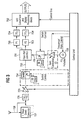
- Figure 1 shows a generally scheme of an I/Q demodulator 21 comprising a five-port junction device 1.
- the proposed topology of figure 1 can be divided into several parts.
- the first part which comprises RF circuitry includes a five-port junction 1 and three power sensors 7, preferably realized by detectors using FET transistors.
- the five-port is only an example for a n-port junction device, n being an integer of 4,5 or 6.
- the five-port 1 is supplied with a modulated RF signal 2 to be demodulated and at a second input 5 it is supplied with a second RF signal 4 from a local oscillator LO which frequency corresponds essentially to the carrier frequency of the first RF signal 2.
- the five-port means 1 comprises three output ports which are connected to three power sensors 7 which detect the power of the RF signals 6 and output the power detection signals 13. Regarding the intended structure and operation of the five-port junction device 1 and the power sensors 7 reference is explicitly made to WO98/08329.
- two “slow” DC-switches 15 are provided which are rerouting the DC signals to one or more low-pass filter banks 14.
- "Slow” in this connection is to be understood lower than in comparison with the symbol duration.
- Each of the filter bank 14 comprises a number of parallel arranged filter whereby each of them may consist of a number of serial connected filter.
- the optional usage of more than one low pass filter bank 14 may be useful for some types of multi-system receivers or future software radio solutions as will be explained later on.
- SDR solutions can be reconfigured (with software downloaded either over-the-air or locally) to operate over a wide frequency band and with a variety of digital modulation formats, such as M-ary phase-shift keying (M-PSK) or M-ary quadrature-amplitude-modulation (M-QAM).
- M-PSK M-ary phase-shift keying
- M-QAM M-ary quadrature-amplitude-modulation
- one filter bank 14 is specified for a video transmission the other for speech transmission requiring a lower bandwidth. In both cases the requisite cut-off frequency of the actual filter bank is different.
- the DC output signal 13 of the power sensor 7 is low-pass-filtered in the filter banks 14 with a cut-off-frequency of B / 2, wherein B is the maximum bandwidth of the RF signal to be demodulated.
- the optional "slow" DC-switches 15 are slow as, when changing operation from one radio system to another, using the same device is usually done by user preferences, so the routing time may be considered as being much more larger compared to the symbol duration. Note that in principle future multi-system solution may need to cope with narrow band signals like GSM having bandwidth of 200 kHz, UMTS with 5 MHz and Hiperlan II having a bandwidth of 20 MHz. In this case an additional filter bank having smaller cut-off-frequency may be advantageous.
- the signals After passing through the low-pass filter bank 14, the signals are then supplied to a further optional low speed DC-switch 15 (which is routing the signals from the optional filter bank 14) and to a fast DC-switch 8 having the function of a multiplexing means.
- the fast DC-switch 8 multiplexes the (n-2) outputs from the low-pass on one single transmission line 22
- the fast DC-switch 8 of the new proposed architecture has a switching time three times shorter (generally (n-2) times) than the symbol duration. When demodulating signals with a shorter symbol duration the switching time is changed accordingly.
- the low-pass filter 20 is followed by a single A/D converter 10 having a sampling rate large enough to accommodate a bandwidth of 3 B / 2.
- the possibility of low-pass-filtering the multiplexed single transmission line 22 may be advantageous in order to minimize the A/D converter 10 requirements (less number of the bits by high sampling speed) and requirements on baseband digital filtering. This reduces actually a typical problem by software radio solution, where adjacent channel interference of narrow band signals has to be minimized.
- DC amplifier 10 Between the low-pass filter 20 and the single A/D converter 10 there is provided a DC amplifier 17. It should be also denoted that optional the DC amplifier 10 may be placed before or after the filter bank 20, but before the fast DC-switch 8.
- the AID converter 10 is supplied with the analog signal which is originating from the fast DC-switch 8.
- the A/D converter 10 is outputting a digitally converted signal to a digital processing unit 19.
- Regarding the digital processing unit 19 reference is explicitly made to WO98/08329.
- All of the devices in the dashed bounded area of figure 1 can be integrated on one single chip.
- Figure 2 shows also a block diagram of an I/Q demodulator comprising in this case a four-port junction device 16.
- the method of operation is related mainly for an operation as PSK demodulator or QAM demodulator.
- the description of figure 2 is nearly the same as that of figure 1.
- A/D converter 10 has a sampling rate able to accommodate the actual system bandwidth of B, rather than 3 B / 2 as in case of the five-port junction 1 able to work as classic I/Q demodulator.
- the proposed solution is advantageous compared to known five-port direct receivers and four-port demodulators because the number of the A/D converters may be reduced to one compared to the state of the art which is shown in figure 3.
- low pass filter bank 14 having different cut-off-frequencies, reduces requirements or number of bits for A/D converters 10 and baseband processing time. Those two steps may provide a good step toward multi-system integration solution and future software radio platform.
- Figure 4 shows further developments of the AID converter 10 and the base band processing block 19.
- the A/D converter 10' may have an adaptive sampling rate. For example in case of signals having a reduced physical bandwidth, the sampling rate of the A/D converter 10' can be reduced correspondingly thus reducing the power consumption of the converter.
- the base band block optionally can be provided with an additional (f.e. analogue) filtering unit 23
Landscapes
- Engineering & Computer Science (AREA)
- Power Engineering (AREA)
- Computer Networks & Wireless Communication (AREA)
- Signal Processing (AREA)
- Digital Transmission Methods That Use Modulated Carrier Waves (AREA)
Abstract
Description
Claims (19)
- I/Q-Demodulator comprising a n-port structure (1) being supplied with a RF signal (2) to be demodulated at a first input (3) and with a second RF-signal (4) at a second input (5),
and outputting n-2 signals (6) to power sensors (7), n being 4, 5 or 6,
characterized by
a multiplexing means (8) for multiplexing low-pass-filtered output signals (9) of the power sensors (7). - I/Q-Demodulator according to claim 1,
characterized in that
it comprises a single A/D converter (10) being supplied with an analog signal (11) originating from the multiplexing means (8) and outputting a digitally converted signal (12) to a digital processing unit (19). - I/Q- Demodulator according to claim 2,
characterized in that
the A/D converter (10') has an adaptive sampling rate. - I/Q- Demodulator according to claim 2 or 3,
characterized in that
the digital processing unit (19) comprises an adaptive baseband filtering unit (23). - I/Q-Demodulator according to anyone of the preceding claims,
characterized in that
the output signal of the power sensors (13) can be selectively passed through different low-pass-filters (14) having different cut-off-frequencies. - I/Q-Demodulator according to anyone of claims 1 to 5,
characterized by
switches (15) for the selection of the low-pass-filters (14). - I/Q-Demodulator according to anyone of the preceding claims,
characterized in that
the n-port is a five-port-junction (1). - I/Q-Demodulator according to anyone of the claims 1 to 6,
characterized in that
the n-port is a four-port-junction (16) and the demodulator is a (M)QAM or (M)PSK demodulator. - I/Q-Demodulator according to anyone of the preceding claims,
characterized in that
the multiplexing means is a DC-switch (8) with a switching time of 1 / n-2 times the symbol duration. - I/Q-Demodulator according to anyone of the preceding claims,
characterized in that
before or after the multiplexing means (8) at least one DC-amplifier (17) is provided. - I/Q-Demodulator according to anyone of the preceding claims,
characterized by
a low-pass-filter (20) following the multiplexing means (8) and having a cut-off-frequency of n-2 / 2B whereby the output signal of the power sensor (13) is low-pass-filtered with a cut-off-frequency of B / 2 and B is the maximum bandwidth of the RF signal (2) to be demodulated. - I/Q-Demodulator according to anyone of the preceding claims,
characterized in that
the n-port (1,16), the power-sensors (7) and said multiplexing means (8) are integrated on one single chip (18). - Software radio device
characterized in that
it comprises an I/Q-demodulator (21) according anyone of the proceeding claims. - Method for I/Q-demodulation
comprising the following steps:inputting a RF-signal (2) to be demodulated in a n-port structure (1),inputting a second RF-signal (4) in a n-port structure (1),detecting (7) the power of n-2 output signals (6) of the n-port structure (1), n being 4,5 or 6,low-pass-filtering (14) the detected power signals (13),multiplexing the low-pass-filtered power signals (9). - Method according to claim 14,
characterized by the step of supplying
a single A/D converter (10) with the multiplexed power signals and outputting a digitally converted signal (12) to a digital processing unit (19). - Method according to claim 15,
characterized by the step of
adapting the sampling rate of the A/D converter (10) depending on the bandwidth of the RF signal (2) to be demodulated. - Method according to claim 14 or 15,
characterized in that
power signals (13) can be selectively filtered (14) with different cut-off-frequencies. - Method according to anyone of claims 14 to 17,
characterized in that
the step of multiplexing is implemented by a DC-switch (8) with a switching time 1 / n-2 of the symbol duration - Method according to anyone of claims 14 to 18,
characterized in that
the multiplexed power signals are low-pass-filtered (20) with a cut-off-frequency of n-2 / 2B whereby the non-multiplexed power signals are low-pass-filtered with the cut-off-frequency of B / 2, where B is the maximum bandwidth of the RF signal (2) to be demodulated.
Priority Applications (4)
| Application Number | Priority Date | Filing Date | Title |
|---|---|---|---|
| EP00114870A EP1172927B1 (en) | 2000-07-11 | 2000-07-11 | Quadrature demodulator using power sensors |
| DE60027284T DE60027284T2 (en) | 2000-07-11 | 2000-07-11 | Quadrature demodulator using power sensors |
| US09/901,273 US7039129B2 (en) | 2000-07-11 | 2001-07-09 | Demodulator structure utilizing DC switches |
| JP2001211276A JP4841068B2 (en) | 2000-07-11 | 2001-07-11 | I/Q demodulation device and I/Q demodulation method |
Applications Claiming Priority (1)
| Application Number | Priority Date | Filing Date | Title |
|---|---|---|---|
| EP00114870A EP1172927B1 (en) | 2000-07-11 | 2000-07-11 | Quadrature demodulator using power sensors |
Publications (2)
| Publication Number | Publication Date |
|---|---|
| EP1172927A1 true EP1172927A1 (en) | 2002-01-16 |
| EP1172927B1 EP1172927B1 (en) | 2006-04-12 |
Family
ID=8169219
Family Applications (1)
| Application Number | Title | Priority Date | Filing Date |
|---|---|---|---|
| EP00114870A Expired - Lifetime EP1172927B1 (en) | 2000-07-11 | 2000-07-11 | Quadrature demodulator using power sensors |
Country Status (4)
| Country | Link |
|---|---|
| US (1) | US7039129B2 (en) |
| EP (1) | EP1172927B1 (en) |
| JP (1) | JP4841068B2 (en) |
| DE (1) | DE60027284T2 (en) |
Cited By (1)
| Publication number | Priority date | Publication date | Assignee | Title |
|---|---|---|---|---|
| EP1376852A1 (en) * | 2002-06-20 | 2004-01-02 | Sony International (Europe) GmbH | I/Q Demodulator based on six-port circuit topologies for mobile receivers |
Families Citing this family (10)
| Publication number | Priority date | Publication date | Assignee | Title |
|---|---|---|---|---|
| DE69829757T2 (en) | 1998-12-18 | 2006-01-12 | Sony International (Europe) Gmbh | Three-gate circuit receiver |
| EP1172927B1 (en) * | 2000-07-11 | 2006-04-12 | Sony Deutschland GmbH | Quadrature demodulator using power sensors |
| US7885409B2 (en) | 2002-08-28 | 2011-02-08 | Rockwell Collins, Inc. | Software radio system and method |
| JP4353052B2 (en) * | 2004-10-04 | 2009-10-28 | 株式会社日立製作所 | Semiconductor integrated circuit |
| US20070223599A1 (en) * | 2005-07-25 | 2007-09-27 | Sysair, Inc., A Delaware Corporation | Cellular PC modem architecture and method of operation |
| JP4182448B2 (en) * | 2006-07-27 | 2008-11-19 | ソニー株式会社 | Receiving device, receiving method, program, and recording medium |
| US7720506B1 (en) | 2006-07-28 | 2010-05-18 | Rockwell Collins, Inc. | System and method of providing antenna specific front ends for aviation software defined radios |
| US7831255B1 (en) | 2006-07-31 | 2010-11-09 | Rockwell Collins, Inc. | System and method of providing automated availability and integrity verification for aviation software defined radios |
| JP4304632B2 (en) * | 2006-10-12 | 2009-07-29 | ソニー株式会社 | Receiving device, receiving method, program, and recording medium |
| US20090267746A1 (en) * | 2008-04-23 | 2009-10-29 | Martec Corporation | Multi-Port Receiver |
Citations (3)
| Publication number | Priority date | Publication date | Assignee | Title |
|---|---|---|---|---|
| EP0805561A2 (en) * | 1996-05-03 | 1997-11-05 | Nokia Mobile Phones Ltd. | A method for implementing a direct conversion receiver with a six-port junction |
| EP0884836A1 (en) * | 1997-06-10 | 1998-12-16 | Her Majesty the Queen in Right of Canada | In-phase quadrature signal regeneration |
| EP0957614A1 (en) * | 1998-05-14 | 1999-11-17 | Sony International (Europe) GmbH | N-port demodulator for PSK or QAM signals |
Family Cites Families (9)
| Publication number | Priority date | Publication date | Assignee | Title |
|---|---|---|---|---|
| US4521728A (en) * | 1982-08-23 | 1985-06-04 | Renato Bosisio | Method and a six port network for use in determining complex reflection coefficients of microwave networks |
| US4870480A (en) * | 1988-06-13 | 1989-09-26 | Rca Licensing Corporation | Subnyquist demodulator as for a television receiver |
| JP2964196B2 (en) * | 1992-06-03 | 1999-10-18 | 富士通株式会社 | Digital quadrature detection demodulator |
| JPH07154439A (en) * | 1993-11-26 | 1995-06-16 | Nec Eng Ltd | Demodulator |
| FI961935A7 (en) * | 1996-05-07 | 1997-11-08 | Nokia Corp | Differential voltage elimination and AM attenuation in a direct conversion receiver |
| FI105367B (en) * | 1997-04-04 | 2000-07-31 | Nokia Mobile Phones Ltd | Attenuation of interference in RF signals |
| EP0896455B1 (en) * | 1997-08-08 | 2006-11-02 | Sony Deutschland GmbH | Non-coherent 6-port receiver |
| AU2274899A (en) * | 1997-12-18 | 1999-07-12 | Sony International (Europe) Gmbh | N-port direct receiver |
| EP1172927B1 (en) * | 2000-07-11 | 2006-04-12 | Sony Deutschland GmbH | Quadrature demodulator using power sensors |
-
2000
- 2000-07-11 EP EP00114870A patent/EP1172927B1/en not_active Expired - Lifetime
- 2000-07-11 DE DE60027284T patent/DE60027284T2/en not_active Expired - Lifetime
-
2001
- 2001-07-09 US US09/901,273 patent/US7039129B2/en not_active Expired - Fee Related
- 2001-07-11 JP JP2001211276A patent/JP4841068B2/en not_active Expired - Fee Related
Patent Citations (3)
| Publication number | Priority date | Publication date | Assignee | Title |
|---|---|---|---|---|
| EP0805561A2 (en) * | 1996-05-03 | 1997-11-05 | Nokia Mobile Phones Ltd. | A method for implementing a direct conversion receiver with a six-port junction |
| EP0884836A1 (en) * | 1997-06-10 | 1998-12-16 | Her Majesty the Queen in Right of Canada | In-phase quadrature signal regeneration |
| EP0957614A1 (en) * | 1998-05-14 | 1999-11-17 | Sony International (Europe) GmbH | N-port demodulator for PSK or QAM signals |
Non-Patent Citations (1)
| Title |
|---|
| J. LI ET. AL.: "A SIX-PORT DIGITAL MILLIMETER WAVE RECEIVER", 1994 IEEE MTT-S INTERNATIONAL MICROWAVE SYMPOSIUM DIGEST, vol. 3, 23 May 1994 (1994-05-23), SAN DIEGO,US, pages 1659 - 1662, XP000512814 * |
Cited By (1)
| Publication number | Priority date | Publication date | Assignee | Title |
|---|---|---|---|---|
| EP1376852A1 (en) * | 2002-06-20 | 2004-01-02 | Sony International (Europe) GmbH | I/Q Demodulator based on six-port circuit topologies for mobile receivers |
Also Published As
| Publication number | Publication date |
|---|---|
| US7039129B2 (en) | 2006-05-02 |
| JP2002077283A (en) | 2002-03-15 |
| EP1172927B1 (en) | 2006-04-12 |
| US20020009161A1 (en) | 2002-01-24 |
| JP4841068B2 (en) | 2011-12-21 |
| DE60027284T2 (en) | 2006-08-31 |
| DE60027284D1 (en) | 2006-05-24 |
Similar Documents
| Publication | Publication Date | Title |
|---|---|---|
| KR100727273B1 (en) | Method and Demodulator for Demodulating Modulated RF Signals | |
| JP4004553B2 (en) | Integrable radio receiver circuit for frequency modulated digital signals | |
| US7260156B2 (en) | Modulation identification device | |
| EP1172927B1 (en) | Quadrature demodulator using power sensors | |
| KR100582855B1 (en) | Non-Coherent 6-Port Receiver | |
| EP0937339B1 (en) | Calibration of n-port receiver | |
| EP1011204B1 (en) | Three-port junction receiver | |
| EP1089445B1 (en) | Three port structure with modulated LO signal | |
| EP1189338A1 (en) | I/Q demodulator device with three power detectors and two A/D converters | |
| EP0957614A1 (en) | N-port demodulator for PSK or QAM signals | |
| US6539215B1 (en) | Down converter and demodulator using a three port junction | |
| EP0926812A1 (en) | Six-port junction device |
Legal Events
| Date | Code | Title | Description |
|---|---|---|---|
| PUAI | Public reference made under article 153(3) epc to a published international application that has entered the european phase |
Free format text: ORIGINAL CODE: 0009012 |
|
| AK | Designated contracting states |
Kind code of ref document: A1 Designated state(s): AT BE CH CY DE DK ES FI FR GB GR IE IT LI LU MC NL PT SE Kind code of ref document: A1 Designated state(s): DE FI FR GB SE |
|
| AX | Request for extension of the european patent |
Free format text: AL;LT;LV;MK;RO;SI |
|
| 17P | Request for examination filed |
Effective date: 20020207 |
|
| AKX | Designation fees paid |
Free format text: DE FI FR GB SE |
|
| 17Q | First examination report despatched |
Effective date: 20050628 |
|
| GRAP | Despatch of communication of intention to grant a patent |
Free format text: ORIGINAL CODE: EPIDOSNIGR1 |
|
| RAP1 | Party data changed (applicant data changed or rights of an application transferred) |
Owner name: SONY CORPORATION Owner name: SONY DEUTSCHLAND GMBH |
|
| RAP1 | Party data changed (applicant data changed or rights of an application transferred) |
Owner name: SONY CORPORATION Owner name: SONY DEUTSCHLAND GMBH |
|
| RAP1 | Party data changed (applicant data changed or rights of an application transferred) |
Owner name: SONY CORPORATION Owner name: SONY DEUTSCHLAND GMBH |
|
| GRAS | Grant fee paid |
Free format text: ORIGINAL CODE: EPIDOSNIGR3 |
|
| GRAA | (expected) grant |
Free format text: ORIGINAL CODE: 0009210 |
|
| AK | Designated contracting states |
Kind code of ref document: B1 Designated state(s): DE FI FR GB SE |
|
| PG25 | Lapsed in a contracting state [announced via postgrant information from national office to epo] |
Ref country code: FI Free format text: LAPSE BECAUSE OF FAILURE TO SUBMIT A TRANSLATION OF THE DESCRIPTION OR TO PAY THE FEE WITHIN THE PRESCRIBED TIME-LIMIT Effective date: 20060412 |
|
| REG | Reference to a national code |
Ref country code: GB Ref legal event code: FG4D |
|
| REF | Corresponds to: |
Ref document number: 60027284 Country of ref document: DE Date of ref document: 20060524 Kind code of ref document: P |
|
| PG25 | Lapsed in a contracting state [announced via postgrant information from national office to epo] |
Ref country code: SE Free format text: LAPSE BECAUSE OF FAILURE TO SUBMIT A TRANSLATION OF THE DESCRIPTION OR TO PAY THE FEE WITHIN THE PRESCRIBED TIME-LIMIT Effective date: 20060712 |
|
| ET | Fr: translation filed | ||
| PLBE | No opposition filed within time limit |
Free format text: ORIGINAL CODE: 0009261 |
|
| STAA | Information on the status of an ep patent application or granted ep patent |
Free format text: STATUS: NO OPPOSITION FILED WITHIN TIME LIMIT |
|
| 26N | No opposition filed |
Effective date: 20070115 |
|
| PGFP | Annual fee paid to national office [announced via postgrant information from national office to epo] |
Ref country code: FR Payment date: 20110729 Year of fee payment: 12 |
|
| PGFP | Annual fee paid to national office [announced via postgrant information from national office to epo] |
Ref country code: GB Payment date: 20120719 Year of fee payment: 13 |
|
| PGFP | Annual fee paid to national office [announced via postgrant information from national office to epo] |
Ref country code: DE Payment date: 20120720 Year of fee payment: 13 |
|
| REG | Reference to a national code |
Ref country code: FR Ref legal event code: ST Effective date: 20130329 |
|
| PG25 | Lapsed in a contracting state [announced via postgrant information from national office to epo] |
Ref country code: FR Free format text: LAPSE BECAUSE OF NON-PAYMENT OF DUE FEES Effective date: 20120731 |
|
| GBPC | Gb: european patent ceased through non-payment of renewal fee |
Effective date: 20130711 |
|
| PG25 | Lapsed in a contracting state [announced via postgrant information from national office to epo] |
Ref country code: DE Free format text: LAPSE BECAUSE OF NON-PAYMENT OF DUE FEES Effective date: 20140201 Ref country code: GB Free format text: LAPSE BECAUSE OF NON-PAYMENT OF DUE FEES Effective date: 20130711 |
|
| REG | Reference to a national code |
Ref country code: DE Ref legal event code: R119 Ref document number: 60027284 Country of ref document: DE Effective date: 20140201 |