EP1172923A1 - Switching voltage regulator, having a driver circuit of a power MOS switch - Google Patents
Switching voltage regulator, having a driver circuit of a power MOS switch Download PDFInfo
- Publication number
- EP1172923A1 EP1172923A1 EP00830481A EP00830481A EP1172923A1 EP 1172923 A1 EP1172923 A1 EP 1172923A1 EP 00830481 A EP00830481 A EP 00830481A EP 00830481 A EP00830481 A EP 00830481A EP 1172923 A1 EP1172923 A1 EP 1172923A1
- Authority
- EP
- European Patent Office
- Prior art keywords
- transistors
- voltage regulator
- power
- regulator according
- driver circuit
- Prior art date
- Legal status (The legal status is an assumption and is not a legal conclusion. Google has not performed a legal analysis and makes no representation as to the accuracy of the status listed.)
- Granted
Links
- 230000003247 decreasing effect Effects 0.000 claims description 4
- 230000007423 decrease Effects 0.000 abstract description 3
- 238000010586 diagram Methods 0.000 description 5
- 230000003071 parasitic effect Effects 0.000 description 4
- 230000000694 effects Effects 0.000 description 2
- 238000005516 engineering process Methods 0.000 description 2
- 239000003990 capacitor Substances 0.000 description 1
- 230000015556 catabolic process Effects 0.000 description 1
- 230000002860 competitive effect Effects 0.000 description 1
- 230000001419 dependent effect Effects 0.000 description 1
- 230000003068 static effect Effects 0.000 description 1
- 238000011144 upstream manufacturing Methods 0.000 description 1
Images

Classifications
-
- H—ELECTRICITY
- H02—GENERATION; CONVERSION OR DISTRIBUTION OF ELECTRIC POWER
- H02M—APPARATUS FOR CONVERSION BETWEEN AC AND AC, BETWEEN AC AND DC, OR BETWEEN DC AND DC, AND FOR USE WITH MAINS OR SIMILAR POWER SUPPLY SYSTEMS; CONVERSION OF DC OR AC INPUT POWER INTO SURGE OUTPUT POWER; CONTROL OR REGULATION THEREOF
- H02M3/00—Conversion of DC power input into DC power output
- H02M3/02—Conversion of DC power input into DC power output without intermediate conversion into AC
- H02M3/04—Conversion of DC power input into DC power output without intermediate conversion into AC by static converters
- H02M3/10—Conversion of DC power input into DC power output without intermediate conversion into AC by static converters using discharge tubes with control electrode or semiconductor devices with control electrode
- H02M3/145—Conversion of DC power input into DC power output without intermediate conversion into AC by static converters using discharge tubes with control electrode or semiconductor devices with control electrode using devices of a triode or transistor type requiring continuous application of a control signal
- H02M3/155—Conversion of DC power input into DC power output without intermediate conversion into AC by static converters using discharge tubes with control electrode or semiconductor devices with control electrode using devices of a triode or transistor type requiring continuous application of a control signal using semiconductor devices only
- H02M3/156—Conversion of DC power input into DC power output without intermediate conversion into AC by static converters using discharge tubes with control electrode or semiconductor devices with control electrode using devices of a triode or transistor type requiring continuous application of a control signal using semiconductor devices only with automatic control of output voltage or current, e.g. switching regulators
- H02M3/158—Conversion of DC power input into DC power output without intermediate conversion into AC by static converters using discharge tubes with control electrode or semiconductor devices with control electrode using devices of a triode or transistor type requiring continuous application of a control signal using semiconductor devices only with automatic control of output voltage or current, e.g. switching regulators including plural semiconductor devices as final control devices for a single load
- H02M3/1584—Conversion of DC power input into DC power output without intermediate conversion into AC by static converters using discharge tubes with control electrode or semiconductor devices with control electrode using devices of a triode or transistor type requiring continuous application of a control signal using semiconductor devices only with automatic control of output voltage or current, e.g. switching regulators including plural semiconductor devices as final control devices for a single load with a plurality of power processing stages connected in parallel
Definitions
- This invention relates to a driver circuit for a MOS power switch incorporated in a switching voltage regulator.
- the setting of this invention is the development of a new family of devices fabricated with BCDV technology, specifically a switching voltage regulator of the step-down type which has a plurality of output currents and is associated with a current loop for a battery charger.
- a switching voltage regulator of the step-down type which has a plurality of output currents and is associated with a current loop for a battery charger.
- Switching voltage regulators are widely utilized in many applications because of their efficiency and precision features. These regulators include, as their basic components: a transistor-based power switch, a loop-back diode, an LC output filter, and an optional current sensor for the battery charger.
- new-generation regulators must have ever higher switching frequencies, so that ever smaller external components can be employed to fill demands for both reduced circuit apace occupation and enhanced cost efficiency.
- these regulators should have the number of their external components reduced to a minimum.
- the frequency increase implies a limited regulator efficiency mainly because of the switching losses of the power switch. Accordingly, the most critical aspect of the regulator carrying out is its circuit portion devoted to driving the power switch, since switching losses are dependent on that portion.
- One of the problems faced by the driver circuits of such power switches is that of achieving a total reduction of both static and dynamic consumption, as well as a control of the current edges so as to minimize electromagnetic disturbance and avoid spurious operation due to any current limiters becoming activated at power-on.
- the current flowing through the power switch exhibits variations of several hundreds Amperes per microsecond, both at power-on and power-off phases.
- the parasitic inductance L of bonding wires may instead be as high as a few tens nH. It follows that, with the current edges being so fast, and because of the values of the parasitic inductance, overvoltages of even 10V may occur at the source and the drain of the power switch.
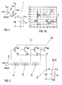
- Figure 1 herein shows, by way of example, the schematic structure of a switching voltage regulator 1 which comprises an N-channel MOS power transistor.
- the driver circuit 2 of such regulator has been optimized to minimize the effect of the time taken to go through the loop-back diode, and in accordance with the teachings of US Patent No. 5,883,505 to the same Applicant.
- the power-on edge is optimized essentially by having the gate of the power switch slowly charged until the loop-back on the diode D is over. This gate is then charged very fast to minimize switching losses.
- the critical switching edge is still the power-off edge, because in order to control the current edge at power-off, it would be necessary to proceed in exactly the opposite way to the power-on situation.
- the power transistor gate would have to be discharged very slowly, and this is unfortunately in conflict with the need of consumption minimization, while also presenting practical difficulties because the power transistor is very large (W of a few tens mm), and when operating close to the threshold value, a few mV variation of the voltage Vgs between the gate and source terminals is enough to produce large variations of the drain Ipower current.
- the drive voltage of the power transistor should therefore be controlled in a very precise manner (within one mV).
- Vgs of the power transistor should be quickly decreased until it nears the threshold value and then should be slowly and accurately varied within one mV.
- Producing a suitable circuit to fill this demand is practically impossible with current BCD technologies; in fact, components would be needed which can respond within a very short time (a few nanoseconds). And even where such components can be made available, it would be necessary to have the voltage at the gate terminal varied very slowly and with a very high precision. (A few mV variation can result in a several Ampere variation occurring in the current.)
- the underlying technical problem of this invention is to contrive a new type of driver circuit for a power transistor, which circuit exhibits appropriate structural and functional features to afford reliable handling of the overvoltage effects, caused by the speed of the current edges during the switching, thereby to obviate the aforementioned drawbacks with reference to the prior art.
- the driver circuit of this invention is to ensure the same speed of response at the power-on as at the power-off edges, at the same time minimizing consumption and avoiding to stress the power transistor gate.
- the principle of this invention is the one of providing the power transistor which forms the power switch by means of a plurality of transistors which are connected to each other in parallel and have scaled dimensions so that they can be independently driven.
- a switching voltage regulator according to this invention is overall and schematically shown at 10 in schematic form.
- This regulator 10 is connected between a first Vin voltage reference of supply and a second ground reference, and comprises a power switch formed by a MOS-type power transistor driven by a driver circuit 2.
- the power switch is intended to drive an electric load on a node OUT, and is associated with a current loop illustrated by a circuit LC having a loop-back diode D associated therewith.
- the power switch is formed of a plurality of power transistors M1, M2, Mn-1 Mn which are connected in parallel to each other.
- each of then transistors M1, M2,..., Mn are driven by a single driver circuit 2 such that the gate terminal of the largest transistor, M1, is discharged very fast, while the gate terminals of the other transistors, M2,..., Mn-1, Mn, of decreasing size are suitably driven by control circuit portions 4, 5, 6..., which are connected between the output of the driver circuit 2 and each respective gate terminal of the corresponding transistor.
- control circuit portions 4, 5, 6,.. By employing these control circuit portions 4, 5, 6,.., the size of the power transistors to be driven is allowed to decrease gradually, while also controlling the leading and trailing edges of the current.
- the equivalent dimensional parameter W of the power switch is greatly reduced because, at power-off, the first transistor M1 with the largest value W1 is readily turned off., All this occurs without affecting the delivered current, since it keeps to be delivered by the remaining transistors M2,..., Mn. Also, with a reduced W, it becomes possible to control, in a finer way and with a wider margin, the edge of the current delivered from the plurality of transistors M1,..., Mn, particularly when approaching the tripping threshold of the whole set of transistors. In fact, the control no longer requires that just a few millivolts be monitored as in the prior art.
- control circuit portions may be implemented, for example, with appropriate delay blocks. Furthermore, it would be perfectly possible to separately drive the n gate terminals and/or move the control of such terminals to a location upstream of the driver circuit 2.
- the control circuit portion is essentially formed essentially with a delay block which is implemented by an RC network comprising a resistor R connected between the gate terminals of the transistors M1, M2, and a parasitic capacitor Cgs present between the gate and source terminals of the second power transistor M2.
- RC network comprising a resistor R connected between the gate terminals of the transistors M1, M2, and a parasitic capacitor Cgs present between the gate and source terminals of the second power transistor M2.
Landscapes
- Engineering & Computer Science (AREA)
- Power Engineering (AREA)
- Dc-Dc Converters (AREA)
- Continuous-Control Power Sources That Use Transistors (AREA)
Abstract
Description
- Figure 1 schematically shows a switching voltage regulator realized according to the prior art.
- Figure 1A shows a diagram reporting, in function of time, the voltage and the current signals present in the regulator of Figure 1.
- Figure 2 shows a schematic view of a switching voltage regulator realized according to the present invention.
- Figure 3 shows a particular embodiment of the regulator of Figure 2.
- Figure 4 shows a diagram reporting, in function of time, the voltage and the current signals present in the regulator of Figure 2 and compared with the signals of the regulator of Figure 1.
Claims (10)
- A switching voltage regulator incorporating a driver circuit of a MOS power switch, characterized in that said MOS switch is formed of a plurality (n) of power transistors (M1, M2, ..., Mn) connected in parallel to each other.
- A voltage regulator according to Claim 1, characterized in that the first (M1) in said plurality of transistors (M1, M2, ..., Mn) has a larger size (W1) than the other transistors.
- A voltage regulator according to Claim 1, characterized in that the sizes (Wi) of the individual power transistors (M1, M2, ..., Mn) are scaled down (W1 * W2 ≥ W3...≥ Wn).
- A voltage regulator according to Claim 1, characterized in that the sizes (Wi) of the individual power transistors (M1, M2, ..., Mn) are scaled down such that:
- A voltage regulator according to Claim 1, characterized in that the first (M1) of said plurality of transistors (M1, M2, ..., Mn) is directly driven directly from said driver circuit (2), while the other translators (M2, ...; Mn) are driven through respective control circuital portions (4, 5, 6,...) connected between the output of the driver circuit (2) and each respective gate terminal of the corresponding transistor.
- A voltage regulator according to Claim 6, characterized in that said control circuital portions (4, 5, 6, ...) are delay blocks.
- A voltage regulator according to Claim 6, characterized in that the transistors (M1 ..., Mn) of said plurality are aranged in a decreasing order of transconductance.
- A voltage regulator according to Claim 1, characterized in that the transistors (M1, ..., Mn) of said plurality are all of the same N-channel or P-channel type.
- A voltage regulator according to Claim 1, characterized in that it comprises a pair of transistors (M1, M2) only, of which the first (M1) is n times larger than the other (M2).
- A voltage regulator according to Claim 9, characterized in that an RC delay block is connected across the gate terminals of said transistor pair (M1, M2).
Priority Applications (3)
| Application Number | Priority Date | Filing Date | Title |
|---|---|---|---|
| EP00830481A EP1172923B1 (en) | 2000-07-10 | 2000-07-10 | Switching voltage regulator, having a driver circuit of a power MOS switch |
| DE60030704T DE60030704T2 (en) | 2000-07-10 | 2000-07-10 | Voltage switching regulator, with a driver circuit of a MOS circuit breaker |
| US09/901,454 US6563293B2 (en) | 2000-07-10 | 2001-07-09 | Switching voltage regulator including a power MOS switch and driver circuit therefor |
Applications Claiming Priority (1)
| Application Number | Priority Date | Filing Date | Title |
|---|---|---|---|
| EP00830481A EP1172923B1 (en) | 2000-07-10 | 2000-07-10 | Switching voltage regulator, having a driver circuit of a power MOS switch |
Publications (2)
| Publication Number | Publication Date |
|---|---|
| EP1172923A1 true EP1172923A1 (en) | 2002-01-16 |
| EP1172923B1 EP1172923B1 (en) | 2006-09-13 |
Family
ID=8175398
Family Applications (1)
| Application Number | Title | Priority Date | Filing Date |
|---|---|---|---|
| EP00830481A Expired - Lifetime EP1172923B1 (en) | 2000-07-10 | 2000-07-10 | Switching voltage regulator, having a driver circuit of a power MOS switch |
Country Status (3)
| Country | Link |
|---|---|
| US (1) | US6563293B2 (en) |
| EP (1) | EP1172923B1 (en) |
| DE (1) | DE60030704T2 (en) |
Cited By (7)
| Publication number | Priority date | Publication date | Assignee | Title |
|---|---|---|---|---|
| EP1424766A1 (en) * | 2002-11-29 | 2004-06-02 | STMicroelectronics S.r.l. | Switching voltage regulator |
| EP1505716A2 (en) | 2003-08-04 | 2005-02-09 | Marvell World Trade Ltd. | Split gate drive scheme to improve reliable voltage operation range |
| DE10355509A1 (en) * | 2003-11-27 | 2005-07-07 | Infineon Technologies Ag | Circuit and method for delayed switching on of an electrical load |
| DE102005029110A1 (en) * | 2005-06-23 | 2006-12-28 | Infineon Technologies Ag | Digital circuit unit for e.g. voltage stabilizer, has power consumption unit which drains current additionally, when change in power consumption of circuit block arranged on chip occurs during load change event |
| EP1986322A1 (en) * | 2007-04-24 | 2008-10-29 | catem DEVELEC GmbH & Co. KG | Semiconductor switch with integrated delay circuit |
| WO2014116841A3 (en) * | 2013-01-28 | 2015-03-19 | Qualcomm Incorporated | Soft turn-off for boost converters |
| DE102014117385B4 (en) | 2014-11-27 | 2021-12-09 | Semikron Elektronik Gmbh & Co. Kg | Power semiconductor circuit and method for operating a power semiconductor circuit |
Families Citing this family (17)
| Publication number | Priority date | Publication date | Assignee | Title |
|---|---|---|---|---|
| US7253540B1 (en) * | 2000-03-15 | 2007-08-07 | Ct Concept Technologie Ag | Method for operating a parallel arrangement of semiconductor power switches |
| WO2002007312A2 (en) * | 2000-07-13 | 2002-01-24 | Isothermal Systems Research, Inc. | Power semiconductor switching devices, power converters, integrated circuit assemblies, integrated circuitry, power current switching methods, methods of forming a power semiconductor switching device, power conversion methods, power semiconductor switching device packaging methods, and methods of forming a power transistor |
| US6825641B2 (en) * | 2003-01-22 | 2004-11-30 | Freescale Semiconductor, Inc. | High efficiency electrical switch and DC-DC converter incorporating same |
| IL160417A (en) * | 2004-02-16 | 2011-04-28 | Mosaid Technologies Inc | Outlet add-on module |
| US20060038543A1 (en) * | 2004-08-23 | 2006-02-23 | Peter Hazucha | DC/DC converters using dynamically-adjusted variable-size switches |
| US7498779B2 (en) * | 2005-01-28 | 2009-03-03 | Broadcom Corporation | Voltage supply interface with improved current sensitivity and reduced series resistance |
| US20080007236A1 (en) * | 2006-07-06 | 2008-01-10 | Alan Elbanhawy | Power converter with segmented power module |
| US8988912B2 (en) * | 2008-10-23 | 2015-03-24 | Leach International Corporation | System and method for emulating an ideal diode in a power control device |
| US20120153909A1 (en) * | 2010-12-16 | 2012-06-21 | International Business Machines Corporation | Hybrid fast-slow passgate control methods for voltage regulators employing high speed comparators |
| TWI400464B (en) * | 2011-02-11 | 2013-07-01 | Etron Technology Inc | Circuit having an external test voltage |
| US8692609B2 (en) * | 2011-02-25 | 2014-04-08 | Peregrine Semiconductor Corporation | Systems and methods for current sensing |
| EP2761384A4 (en) * | 2011-09-30 | 2015-11-04 | Intel Corp | Apparatus and method to improve integrated voltage regulators |
| US9667168B2 (en) * | 2015-05-12 | 2017-05-30 | Integrated Device Technology, Inc. | System and method for synchronous rectification with enhanced detection of small currents |
| JP2019158573A (en) * | 2018-03-13 | 2019-09-19 | 株式会社東芝 | Semiconductor integrated circuit |
| US10298134B1 (en) * | 2018-03-19 | 2019-05-21 | Dialog Semiconductor (Uk) Limited | Switching converter soft start method using scaled switch size |
| AU2020264140B2 (en) * | 2019-04-24 | 2026-02-26 | Commonwealth Scientific And Industrial Research Organisation | Short-circuit mitigation device |
| US11018663B2 (en) * | 2019-09-20 | 2021-05-25 | Texas Instruments Incorporated | Linear switch circuits and methods |
Citations (4)
| Publication number | Priority date | Publication date | Assignee | Title |
|---|---|---|---|---|
| US4616142A (en) * | 1984-12-31 | 1986-10-07 | Sundstrand Corporation | Method of operating parallel-connected semiconductor switch elements |
| EP0581016A1 (en) * | 1992-06-26 | 1994-02-02 | Kollmorgen Corporation | Apparatus and method for forced sharing of parallel MOSFET switching losses |
| JPH09285120A (en) * | 1996-04-19 | 1997-10-31 | Oki Electric Ind Co Ltd | Main switch control circuit of power source equipment |
| US5949158A (en) * | 1997-05-05 | 1999-09-07 | Gerhard Kurz | Method and arrangement for controlling the output of electrical consumers connected to an AC line voltage |
Family Cites Families (10)
| Publication number | Priority date | Publication date | Assignee | Title |
|---|---|---|---|---|
| NO159898C (en) * | 1985-12-19 | 1989-02-15 | Alcatel Stk As | STROEMFORSYNING. |
| US5012178A (en) * | 1990-03-19 | 1991-04-30 | Triquint Semiconductor, Inc. | Low noise DAC current source topology |
| JPH088457B2 (en) * | 1992-12-08 | 1996-01-29 | 日本電気株式会社 | Differential amplifier circuit |
| US6084790A (en) * | 1999-01-07 | 2000-07-04 | Astec International Limited | Circuit to ensure equal current sharing and switching losses between parallel power devices |
| US6316956B1 (en) * | 1999-10-22 | 2001-11-13 | Motorola, Inc. | Multiple redundant reliability enhancement method for integrated circuits and transistors |
| US6229289B1 (en) * | 2000-02-25 | 2001-05-08 | Cadence Design Systems, Inc. | Power converter mode transitioning method and apparatus |
| JP2001298945A (en) * | 2000-04-17 | 2001-10-26 | Taiyo Yuden Co Ltd | Driving method for power circuit, power circuit, and electronic part for power supply |
| US6222353B1 (en) * | 2000-05-31 | 2001-04-24 | Philips Semiconductors, Inc. | Voltage regulator circuit |
| US6249111B1 (en) * | 2000-06-22 | 2001-06-19 | Intel Corporation | Dual drive buck regulator |
| US6362606B1 (en) * | 2000-09-12 | 2002-03-26 | Silicon Laboratories, Inc | Method and apparatus for regulating a voltage |
-
2000
- 2000-07-10 DE DE60030704T patent/DE60030704T2/en not_active Expired - Lifetime
- 2000-07-10 EP EP00830481A patent/EP1172923B1/en not_active Expired - Lifetime
-
2001
- 2001-07-09 US US09/901,454 patent/US6563293B2/en not_active Expired - Lifetime
Patent Citations (4)
| Publication number | Priority date | Publication date | Assignee | Title |
|---|---|---|---|---|
| US4616142A (en) * | 1984-12-31 | 1986-10-07 | Sundstrand Corporation | Method of operating parallel-connected semiconductor switch elements |
| EP0581016A1 (en) * | 1992-06-26 | 1994-02-02 | Kollmorgen Corporation | Apparatus and method for forced sharing of parallel MOSFET switching losses |
| JPH09285120A (en) * | 1996-04-19 | 1997-10-31 | Oki Electric Ind Co Ltd | Main switch control circuit of power source equipment |
| US5949158A (en) * | 1997-05-05 | 1999-09-07 | Gerhard Kurz | Method and arrangement for controlling the output of electrical consumers connected to an AC line voltage |
Non-Patent Citations (1)
| Title |
|---|
| PATENT ABSTRACTS OF JAPAN vol. 1998, no. 02 30 January 1998 (1998-01-30) * |
Cited By (13)
| Publication number | Priority date | Publication date | Assignee | Title |
|---|---|---|---|---|
| US6998827B2 (en) | 2002-11-29 | 2006-02-14 | Stmicroelectronics S.R.L. | Switching voltage regulator with negative temperature compensation |
| EP1424766A1 (en) * | 2002-11-29 | 2004-06-02 | STMicroelectronics S.r.l. | Switching voltage regulator |
| US7737666B2 (en) | 2003-08-04 | 2010-06-15 | Marvell World Trade Ltd. | Split gate drive scheme to improve reliable voltage operation range |
| EP1505716A3 (en) * | 2003-08-04 | 2006-11-22 | Marvell World Trade Ltd. | Split gate drive scheme to improve reliable voltage operation range |
| EP1505716A2 (en) | 2003-08-04 | 2005-02-09 | Marvell World Trade Ltd. | Split gate drive scheme to improve reliable voltage operation range |
| DE10355509A1 (en) * | 2003-11-27 | 2005-07-07 | Infineon Technologies Ag | Circuit and method for delayed switching on of an electrical load |
| US7183816B2 (en) | 2003-11-27 | 2007-02-27 | Infineon Technologies Ag | Circuit and method for switching an electrical load on after a delay |
| DE102005029110A1 (en) * | 2005-06-23 | 2006-12-28 | Infineon Technologies Ag | Digital circuit unit for e.g. voltage stabilizer, has power consumption unit which drains current additionally, when change in power consumption of circuit block arranged on chip occurs during load change event |
| US7603572B2 (en) | 2005-06-23 | 2009-10-13 | Infineon Technologies Ag | Voltage stabilizer stabilizing the voltage of a power line wherein power consumption elements are individually activated based on a quantity of currents to be drained |
| EP1986322A1 (en) * | 2007-04-24 | 2008-10-29 | catem DEVELEC GmbH & Co. KG | Semiconductor switch with integrated delay circuit |
| WO2014116841A3 (en) * | 2013-01-28 | 2015-03-19 | Qualcomm Incorporated | Soft turn-off for boost converters |
| US9124231B2 (en) | 2013-01-28 | 2015-09-01 | Qualcomm, Inc. | Soft turn-off for boost converters |
| DE102014117385B4 (en) | 2014-11-27 | 2021-12-09 | Semikron Elektronik Gmbh & Co. Kg | Power semiconductor circuit and method for operating a power semiconductor circuit |
Also Published As
| Publication number | Publication date |
|---|---|
| EP1172923B1 (en) | 2006-09-13 |
| DE60030704T2 (en) | 2007-10-04 |
| DE60030704D1 (en) | 2006-10-26 |
| US6563293B2 (en) | 2003-05-13 |
| US20020021114A1 (en) | 2002-02-21 |
Similar Documents
| Publication | Publication Date | Title |
|---|---|---|
| EP1172923B1 (en) | Switching voltage regulator, having a driver circuit of a power MOS switch | |
| US9035625B2 (en) | Common cascode routing bus for high-efficiency DC-to-DC conversion | |
| CN110958003B (en) | Adaptive gate driver | |
| US8634171B2 (en) | Over voltage protection of a switching converter | |
| US8212536B2 (en) | Stacked NMOS DC-to-DC power conversion | |
| EP1639693B1 (en) | Dead time control in a switching circuit | |
| US7746042B2 (en) | Low-noise DC/DC converter with controlled diode conduction | |
| US8294438B2 (en) | Circuit and method for phase shedding with reverse coupled inductor | |
| US6897707B2 (en) | Isolated FET drive utilizing Zener diode based systems, methods and apparatus | |
| IL257786B2 (en) | Low voltage sub-nanosecond pulsed current driver ic for high-resolution lidar applications | |
| EP4120567B1 (en) | Cascaded gate driver outputs for power conversion circuits | |
| US6373732B1 (en) | Apparatus and method for parallel synchronous power converters | |
| CN115411931A (en) | Dynamic voltage division ratio charge pump switch | |
| US10305473B2 (en) | Control circuitry for controlling a set of switches | |
| US5596489A (en) | Capacitive transformer having a switch responsive to clock signals | |
| Ma | Driving GaN power transistors | |
| CN212627663U (en) | Power circuits and circuits including half-bridge drivers | |
| CN101019320A (en) | DC/DC converter with dynamic offset compensation | |
| US11196348B2 (en) | Methods and systems of controlling switching frequency of a switching power converter | |
| CN111585428B (en) | Surge current limiter | |
| US20110121805A1 (en) | Active Power Switch Topology for Switching Regulators | |
| US8569811B1 (en) | Self clamping FET devices in circuits using transient sources | |
| KR20250089458A (en) | Fast Fly Capacitor Pre-Charging Circuit | |
| US7564231B2 (en) | Switching power supply source | |
| CN113922794B (en) | Short circuit protection circuit |
Legal Events
| Date | Code | Title | Description |
|---|---|---|---|
| PUAI | Public reference made under article 153(3) epc to a published international application that has entered the european phase |
Free format text: ORIGINAL CODE: 0009012 |
|
| AK | Designated contracting states |
Kind code of ref document: A1 Designated state(s): DE FR GB IT Kind code of ref document: A1 Designated state(s): AT BE CH CY DE DK ES FI FR GB GR IE IT LI LU MC NL PT SE |
|
| AX | Request for extension of the european patent |
Free format text: AL;LT;LV;MK;RO;SI |
|
| 17P | Request for examination filed |
Effective date: 20020402 |
|
| AKX | Designation fees paid |
Free format text: DE FR GB IT |
|
| 17Q | First examination report despatched |
Effective date: 20040916 |
|
| GRAP | Despatch of communication of intention to grant a patent |
Free format text: ORIGINAL CODE: EPIDOSNIGR1 |
|
| RIC1 | Information provided on ipc code assigned before grant |
Ipc: 7H 03K 17/12 A Ipc: 7H 02M 3/158 B |
|
| GRAJ | Information related to disapproval of communication of intention to grant by the applicant or resumption of examination proceedings by the epo deleted |
Free format text: ORIGINAL CODE: EPIDOSDIGR1 |
|
| GRAP | Despatch of communication of intention to grant a patent |
Free format text: ORIGINAL CODE: EPIDOSNIGR1 |
|
| GRAS | Grant fee paid |
Free format text: ORIGINAL CODE: EPIDOSNIGR3 |
|
| GRAA | (expected) grant |
Free format text: ORIGINAL CODE: 0009210 |
|
| AK | Designated contracting states |
Kind code of ref document: B1 Designated state(s): DE FR GB IT |
|
| PG25 | Lapsed in a contracting state [announced via postgrant information from national office to epo] |
Ref country code: IT Free format text: LAPSE BECAUSE OF FAILURE TO SUBMIT A TRANSLATION OF THE DESCRIPTION OR TO PAY THE FEE WITHIN THE PRESCRIBED TIME-LIMIT;WARNING: LAPSES OF ITALIAN PATENTS WITH EFFECTIVE DATE BEFORE 2007 MAY HAVE OCCURRED AT ANY TIME BEFORE 2007. THE CORRECT EFFECTIVE DATE MAY BE DIFFERENT FROM THE ONE RECORDED. Effective date: 20060913 |
|
| REG | Reference to a national code |
Ref country code: GB Ref legal event code: FG4D |
|
| REF | Corresponds to: |
Ref document number: 60030704 Country of ref document: DE Date of ref document: 20061026 Kind code of ref document: P |
|
| ET | Fr: translation filed | ||
| PLBE | No opposition filed within time limit |
Free format text: ORIGINAL CODE: 0009261 |
|
| STAA | Information on the status of an ep patent application or granted ep patent |
Free format text: STATUS: NO OPPOSITION FILED WITHIN TIME LIMIT |
|
| 26N | No opposition filed |
Effective date: 20070614 |
|
| GBPC | Gb: european patent ceased through non-payment of renewal fee |
Effective date: 20070710 |
|
| PG25 | Lapsed in a contracting state [announced via postgrant information from national office to epo] |
Ref country code: GB Free format text: LAPSE BECAUSE OF NON-PAYMENT OF DUE FEES Effective date: 20070710 |
|
| PGFP | Annual fee paid to national office [announced via postgrant information from national office to epo] |
Ref country code: DE Payment date: 20120625 Year of fee payment: 13 Ref country code: FR Payment date: 20120806 Year of fee payment: 13 |
|
| REG | Reference to a national code |
Ref country code: FR Ref legal event code: ST Effective date: 20140331 |
|
| PG25 | Lapsed in a contracting state [announced via postgrant information from national office to epo] |
Ref country code: DE Free format text: LAPSE BECAUSE OF NON-PAYMENT OF DUE FEES Effective date: 20140201 |
|
| REG | Reference to a national code |
Ref country code: DE Ref legal event code: R119 Ref document number: 60030704 Country of ref document: DE Effective date: 20140201 |
|
| PG25 | Lapsed in a contracting state [announced via postgrant information from national office to epo] |
Ref country code: FR Free format text: LAPSE BECAUSE OF NON-PAYMENT OF DUE FEES Effective date: 20130731 |