EP1172789A2 - Display power supply - Google Patents
Display power supply Download PDFInfo
- Publication number
- EP1172789A2 EP1172789A2 EP01106130A EP01106130A EP1172789A2 EP 1172789 A2 EP1172789 A2 EP 1172789A2 EP 01106130 A EP01106130 A EP 01106130A EP 01106130 A EP01106130 A EP 01106130A EP 1172789 A2 EP1172789 A2 EP 1172789A2
- Authority
- EP
- European Patent Office
- Prior art keywords
- voltage
- circuit
- power supply
- power
- capacitor
- Prior art date
- Legal status (The legal status is an assumption and is not a legal conclusion. Google has not performed a legal analysis and makes no representation as to the accuracy of the status listed.)
- Withdrawn
Links
- 239000003990 capacitor Substances 0.000 claims abstract description 47
- 238000010586 diagram Methods 0.000 description 10
- 230000008878 coupling Effects 0.000 description 7
- 238000010168 coupling process Methods 0.000 description 7
- 238000005859 coupling reaction Methods 0.000 description 7
- 230000003287 optical effect Effects 0.000 description 7
- 230000002459 sustained effect Effects 0.000 description 2
- 230000004913 activation Effects 0.000 description 1
- 230000002939 deleterious effect Effects 0.000 description 1
- 230000000977 initiatory effect Effects 0.000 description 1
- 239000004973 liquid crystal related substance Substances 0.000 description 1
- 238000004519 manufacturing process Methods 0.000 description 1
- 238000000034 method Methods 0.000 description 1
- 238000012163 sequencing technique Methods 0.000 description 1
- 239000000725 suspension Substances 0.000 description 1
Images




Classifications
-
- H—ELECTRICITY
- H02—GENERATION; CONVERSION OR DISTRIBUTION OF ELECTRIC POWER
- H02M—APPARATUS FOR CONVERSION BETWEEN AC AND AC, BETWEEN AC AND DC, OR BETWEEN DC AND DC, AND FOR USE WITH MAINS OR SIMILAR POWER SUPPLY SYSTEMS; CONVERSION OF DC OR AC INPUT POWER INTO SURGE OUTPUT POWER; CONTROL OR REGULATION THEREOF
- H02M3/00—Conversion of DC power input into DC power output
- H02M3/22—Conversion of DC power input into DC power output with intermediate conversion into AC
- H02M3/24—Conversion of DC power input into DC power output with intermediate conversion into AC by static converters
- H02M3/28—Conversion of DC power input into DC power output with intermediate conversion into AC by static converters using discharge tubes with control electrode or semiconductor devices with control electrode to produce the intermediate AC
- H02M3/325—Conversion of DC power input into DC power output with intermediate conversion into AC by static converters using discharge tubes with control electrode or semiconductor devices with control electrode to produce the intermediate AC using devices of a triode or a transistor type requiring continuous application of a control signal
- H02M3/335—Conversion of DC power input into DC power output with intermediate conversion into AC by static converters using discharge tubes with control electrode or semiconductor devices with control electrode to produce the intermediate AC using devices of a triode or a transistor type requiring continuous application of a control signal using semiconductor devices only
- H02M3/338—Conversion of DC power input into DC power output with intermediate conversion into AC by static converters using discharge tubes with control electrode or semiconductor devices with control electrode to produce the intermediate AC using devices of a triode or a transistor type requiring continuous application of a control signal using semiconductor devices only in a self-oscillating arrangement
- H02M3/3381—Conversion of DC power input into DC power output with intermediate conversion into AC by static converters using discharge tubes with control electrode or semiconductor devices with control electrode to produce the intermediate AC using devices of a triode or a transistor type requiring continuous application of a control signal using semiconductor devices only in a self-oscillating arrangement using a single commutation path
-
- H—ELECTRICITY
- H02—GENERATION; CONVERSION OR DISTRIBUTION OF ELECTRIC POWER
- H02M—APPARATUS FOR CONVERSION BETWEEN AC AND AC, BETWEEN AC AND DC, OR BETWEEN DC AND DC, AND FOR USE WITH MAINS OR SIMILAR POWER SUPPLY SYSTEMS; CONVERSION OF DC OR AC INPUT POWER INTO SURGE OUTPUT POWER; CONTROL OR REGULATION THEREOF
- H02M1/00—Details of apparatus for conversion
- H02M1/36—Means for starting or stopping converters
Definitions
- the present invention relates to power supply and, more particularly, to a power supply suitable for display devices.
- PDPs plasma display panels
- the two types of voltages are a drive voltage of several tens to several ten thousands of volts for turning on the display elements and a control voltage of several volts employed as the power supply voltage for a control circuit of the display elements.
- FIG.1 is a circuit block diagram illustrating the configuration of the power supply of the first prior art.
- a power supply 109 shown in Fig.1 includes a rectifier circuit 102 connected to an external commercial power source 100; switches 104a, 104b disposed between the commercial power source 100 and the rectifier circuit 102; a capacitor 105 connected to the output of the rectifier circuit 102; and a DC/DC converter 101, connected to the commercial power source 100 via the rectifier circuit 102, for generating output voltages of +5V and +35V.
- the power supply 109 also includes an output terminal 106a, connected to the output of the DC/DC converter 101, for providing an output voltage of +5V; an output terminal 106b, connected to the output of the DC/DC converter 101, for providing an output voltage of +35V; an optical coupling isolator 103 for outputting a signal in accordance with the input voltage of the DC/DC converter 101; and a switching circuit 107 connected to the output of the optical coupling isolator 103 and including a photo MOS relay 108 which is opened or closed in accordance with a signal outputted from the optical coupling isolator 103.
- the switching circuit 107 is connected between the DC/DC converter 101 and the output terminal 106b to open or close the connection between the DC/DC converter 101 and the output terminal 106b.
- the optical coupling isolator 103 detects the input voltage of the DC/DC converter 101. Shutting down the power supply output from the commercial power source 100 will cause the optical coupling isolator 103 to output a signal to the photo MOS relay 108. This will cause the photo MOS relay 108 to be opened forcedly, the switching circuit 107 to be opened, and the voltage of 35V to be shut down which needs to be disabled quickly. This provides the aforementioned sequence of disabling first the drive voltage and then disabling the control voltage.
- Fig.2 is a circuit block diagram illustrating the configuration of the LCD incorporating the power supply of the second prior art.
- the LCD shown in Fig.2 includes batteries 211, a DC/DC converter 214 for converting the output voltage of the batteries 211 to a control voltage Vcc, and a power switching transistor 212 connected between the batteries 211 and the DC/DC converter 214.
- the LCD also includes a power control IC 213 connected to the base of the power switching transistor 212 via a resistor R204; a timer 215 connected to the power control IC 213; an inverter 216 connected to the timer 215; and an AND gate 217, the input of which is connected to the inverter 216 and a delay device 201A and the output of which is connected to the base of an LCD power front-stage transistor 219 via a resistor R205.
- a power control IC 213 connected to the base of the power switching transistor 212 via a resistor R204
- a timer 215 connected to the power control IC 213
- an inverter 216 connected to the timer 215
- an AND gate 217 the input of which is connected to the inverter 216 and a delay device 201A and the output of which is connected to the base of an LCD power front-stage transistor 219 via a resistor R205.
- the LCD also includes an LCD power rear-stage transistor 220, the collector of which is connected to the power switching transistor 212 and the base of which is connected to the collector of the LCD power front-stage transistor 219 via a resistor R206; a device logic portion 201E to which the control voltage Vcc is supplied from the DC/DC converter 214: and a DC/DC converter 218 for converting the output voltage of the batteries 211 to a drive voltage Vee.
- the LCD further includes an LCD panel portion 201F to which the drive voltage Vee is supplied from the DC/DC converter 218; a delay device 201A which is connected between the output terminal of the DC/DC converter 214 and the ground and which includes a resistor and a capacitor; and an FET 201D driven by the delay device 201A.
- the device logic portion 201E is the control circuit of the LCD panel portion 201F.
- the LCD has a capacitor C201 connected to the DC/DC converter 218.
- the LCD is provided with a resistor R208 connected to the higher potential side of the FET 201D in series therewith.
- a resistor R207 is connected between the collector of the LCD power front-stage transistor 219 and the FET 201D.
- the delay device 201A causes the FET 201D to conduct. This allows the drive voltage Vee to be disabled forcedly prior to the control voltage Vcc, thereby providing the aforementioned sequencing.
- the power supply of the first prior art has a problem of requiring the employment of the optical coupling isolator 103 and the photo MOS relay 108, thereby leading to an increase in cost of the power supply.
- the power supply of the second prior art is a power circuit for an LCD display device and therefore supplies a drive voltage of several tens of volts.
- a drive voltage of several hundreds to several ten thousands of volts is required for discharge-type display devices such as CRTs (Cathode Ray Tubes) or PDPs.
- CRTs Cathode Ray Tubes
- PDPs PDPs
- Fig.3 is a graph illustrating the time dependency of the output voltage of the power supply of the second prior art.
- the drive voltage Vee and the control voltage Vcc increase together after the power output has been turned on and decrease together after the power has been turned off.
- the power supply of the second prior art allows the control voltage Vcc to be disabled in a short period of time.
- the power supply has the capacitor C201 of a large-capacity connected to the output terminal of the DC/DC converter 218. This will not allow the power accumulated in the capacitor C201 to be discharged quickly, causing the drive voltage Vee to be sustained at a high voltage for a long period of time.
- the drive voltage Vee as high as several hundreds to several ten thousands of volts would be applied to the drive and control circuits of the display device to cause damage to these circuits in some cases.
- a discharge circuit would be required to discharge the power accumulated in the capacitor C201 when the power supply output is shut down.
- a discharge current of high voltage and high current would pass through the resistor R208 and the FET 201D of the second prior art, which constitute the discharge circuit. This makes it necessary to provide an extremely high allowable voltage for these components. This causes a problem of significantly increasing the cost for manufacturing the power supply.
- a power supply comprises a first power circuit, supplied with a voltage from an external power source, for outputting a first voltage; a first capacitor for being charged with said first voltage; and a second power circuit, supplied with a voltage from said external power source, for outputting a second voltage lower than said first voltage.
- the power supply also comprises a voltage converter circuit, an input terminal thereof being connected to a high voltage side of said first capacitor, and an output terminal thereof being connected to an output terminal of said second power circuit, wherein power accumulated in said first capacitor is converted to a voltage to be supplied to the output terminal of said second power circuit when said external power source stops supplying the voltage.
- the power accumulated in the first capacitor is discharged to the output of the second power circuit via the voltage converter circuit after the power supply output has been shut down.
- this allows the first voltage to be disabled quickly in a short period of time and sustain the second voltage for a fixed period of time.
- This makes it possible to disable the drive voltage prior to the control voltage in a discharge-type display device incorporating the power supply according to the present invention when the first voltage is employed as the drive voltage for driving the display device and the second voltage is employed as the control voltage for controlling the display device.
- the voltage converter circuit converts the power accumulated in the first capacitor to the second voltage for supply, thereby obviating the need of a discharge circuit of a large capacity which is essential to the conventional power supply. This makes it possible to provide the power supply at a reduced cost.
- Another power supply according to the present invention comprises a first power circuit, supplied with a voltage from an external power source, for outputting a first voltage; a first capacitor for being charged with said first voltage; and a second power circuit, supplied with a voltage from said external power source, for outputting a second voltage lower than said first voltage.
- the power supply according to the present invention also comprises a voltage converter circuit, an input terminal thereof being connected to a high voltage side of said first capacitor, and an output terminal thereof being connected to an input terminal of said second power circuit, wherein power accumulated in said first capacitor is converted to a voltage to be supplied to the output terminal of said second power circuit when said external power source stops supplying the voltage.
- the present invention allows the power accumulated in the first capacitor to be discharged to the input of the second power circuit via the voltage converter circuit, thereby making it possible to further stabilize the second voltage.
- Fig.4 is a circuit block diagram illustrating the configuration of a power supply according to the first embodiment of the present invention and a display device incorporating the power supply.
- a PDP (Plasma Display Panel) power circuit 1 (power supply) shown in Fig.4 is connected between a commercial power source 99 and a PDP display device 50 and converts an AC power supply voltage Vp supplied from the commercial power source 99 to a DC drive voltage Vdd and a DC control voltage Vcc, which are in turn supplied to the PDP display device 50.
- the PDP display device 50 includes a PDP drive circuit 50a for converting an image signal Sv supplied externally to a drive signal for driving PDP display cells 50c; a PDP control circuit 50b for controlling the operation of the PDP drive circuit 50a; and the PDP display cells 50c used for display in accordance with the drive signal supplied from the PDP drive circuit 50a.
- the PDP power circuit 1 includes a rectifier circuit 2 connected to the commercial power source 99; a high voltage power circuit 10, connected to the rectifier circuit 2, for outputting a voltage Voh; a capacitor C1 connected between an output terminal of the high voltage power circuit 10 and the ground potential; and a low voltage power circuit 20, connected to the rectifier circuit 2, for outputting a voltage Vol which is lower than the voltage Voh.
- the PDP power circuit 1 also includes a capacitor C2 connected between an output terminal of the low voltage power circuit 20 and the ground potential; a DC/DC converter 30 connected to the capacitor C1; a voltage detector circuit 31, connected between an output terminal of the high voltage power circuit 10 and the ground potential, for outputting an operation control signal Sc to the DC/DC converter 30; and a diode D3 connected between the DC/DC converter 30 and the capacitor C2.
- the rectifier circuit 2 includes a diode bridge or the like.
- the rectifier circuit 2 converts the AC power supply voltage Vp supplied from the commercial power source 99 to a DC voltage.
- the high voltage power circuit 10 includes a switching control circuit 11, a switching transformer 12, a switching transistor TR1, and a diode D1.
- the high voltage power circuit 10 is a switching power circuit for converting the power supply voltage Vp rectified by the rectifier circuit 2 to the voltage Voh for output. Under a steady state, the output voltage Voh acts as the drive voltage Vdd to be applied to the PDP drive circuit 50a. In this embodiment, the drive voltage Vdd is set at 170V.
- the capacitor C1 is connected between the output terminal of the high voltage power circuit 10 and the ground potential and becomes charged by the output voltage Voh of the high voltage power circuit 10.
- the low voltage power circuit 20 includes a switching control circuit 21, a switching transformer 22, a switching transistor TR2, and a diode D2.
- the low voltage power circuit 20 is a switching power circuit for converting the power supply voltage V p rectified by the rectifier circuit 2 to the voltage Vol for output. Under a steady state, the output voltage Vol acts as the control voltage Vcc to be applied to the PDP control circuit 50b. In this embodiment, the control voltage Vcc is set at 5V.
- the capacitor C2 is connected between an output terminal of the low voltage power circuit 20 and the ground potential.
- the capacitor C2 is preferably adapted to have a large capacity of several thousands ⁇ F to provide an extended output period of time of the control voltage Vcc.
- the DC/DC converter 30 is connected between the output terminal of the high voltage power circuit 10 and the ground potential and converts the voltage Voh of the high voltage power circuit 10 to the voltage Vol, then supplying the voltage Vol to the capacitor C2 via the diode D3.
- the DC/DC converter 30 can employ an arbitrary circuit scheme such as an isolating type DC/DC converter.
- the diode D3 is connected between the output terminal of the DC/DC converter 30 and the output terminal of the low voltage power circuit 20 to be forward biased in the direction from the DC/DC converter 30 to the low voltage power circuit 20, preventing back-flow of current from the output terminal of the low voltage power circuit 20 to the output terminal of the DC/DC converter 30.
- the voltage detector circuit 31 is connected between the output terminal of the high voltage power circuit 10 and the ground potential.
- the voltage detector circuit 31 detects the output voltage Voh of the high voltage power circuit 10 to compare the voltage Voh with a voltage set point Vs which has been set in advance therein.
- the voltage set point Vs is 160V at the drive voltage Vdd of 170V.
- the voltage detector circuit 31 initiates outputting the operation control signal Sc when the voltage Voh of the high voltage power circuit 10 has dropped from a rating voltage of the drive voltage Vdd (170V) to the voltage set point Vs (160V).
- the voltage detector circuit 31 stops outputting the operation control signal Sc when the output voltage Voh of the high voltage power circuit 10 has dropped to the minimum operation voltage Vlow of the DC/DC converter 30.
- the voltage detector circuit 31 can employ various types of known voltage comparison circuits such as one utilizing a voltage comparator circuit or the like.
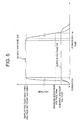
- Fig.5 is a graph illustrating the time dependency of the output voltage of the power circuit according to this embodiment.
- the voltage detector circuit 31 When the output voltage Voh has dropped to the voltage set point Vs (160V), the voltage detector circuit 31 outputs the operation control signal Sc to activate the DC/DC converter 30.
- the initiation of the operation of the DC/DC converter 30 causes the power accumulated in the capacitor C1 to decrease rapidly, thus causing the output voltage Voh to drop rapidly.
- the output of the control voltage Vcc can be sustained up to time Te at which the output voltage Voh becomes to the minimum operation voltage Vlow of the DC/DC converter 30.
- this embodiment upon shutting down of the power supply output, this embodiment makes it possible to convert the power accumulated in the capacitor Cl to the control voltage Vcc for discharge. This makes it possible to implement the sequence of disabling quickly the drive voltage Vdd of the display device prior to the control voltage Vcc. This also makes it possible to provide an extended period of time for the output of the control voltage Vcc even after the power supply output has been shut down.
- Fig.6 is a circuit block diagram illustrating the configuration of a power supply according to a second embodiment of the present invention and a display device incorporating the power supply.
- a PDP power circuit la shown in Fig.6 excludes the voltage detector circuit 31 from the PDP power circuit 1 shown in Fig.4 and has the PDP control circuit 50b connected to the DC/DC converter 30 to allow the PDP control circuit 50b to control the output of the operation control signal Sc.
- the components of the PDP power circuit la according to this embodiment other than those mentioned above remain the same as those of the PDP power circuit 1 shown in Fig.4.
- the PDP power circuit la When the output voltage Voh has dropped below the voltage set point Vs, the PDP power circuit la according to this embodiment allows the PDP control circuit 50b to output the operation control signal Sc to the DC/DC converter 30 to activate the DC/DC converter 30. On the other hand, the PDP control circuit 50b stops outputting the operation control signal Sc when the output voltage Voh of the high voltage power circuit 10 has dropped to the minimum operation voltage Vlow of the DC/DC converter 30.
- the operations of the PDP power circuit la according to this embodiment other than that mentioned above are the same as those of the PDP power circuit 1 shown in Fig.4.
- the aforementioned PDP power circuit 1 is provided with the voltage detector circuit 31 to detect the output voltage Voh of the high voltage power circuit 10 in order to control the DC/DC converter 30.
- the PDP power circuit la allows the PDP control circuit 50b to output the operation control signal Sc in order to control the activation and suspension of the DC/DC converter 30. This makes it possible to allow the PDP control circuit 50b to control the operation of the PDP power circuit 1 and the PDP display device 50.
- this configuration makes it possible to implement the control of power supply output using the control circuit or the like of the PDP display device without the voltage detector circuit 31 (see Fig.4).
- Fig.7 is a circuit block diagram illustrating the configuration of a power supply according to a third embodiment of the present invention and a display device incorporating the power supply.
- a capacitor C3 is connected an input terminal of the low voltage power circuit 20.
- the capacitor C3 is charged with an input voltage of the low voltage power circuit 20.
- a diode D3 is also connected between the DC/DC converter 30 and the capacitor C3 so as to be forward biased in the direction from the DC/DC converter 30 to the capacitor C3.
- a diode D4 for preventing back-flow is also connected in the direction from the input of the high voltage power circuit 10 to the input of the low voltage power circuit 20.
- the components of the PDP power circuit 1b according to this embodiment other than those mentioned above are the same as those of the PDP power circuit 1 according to the aforementioned first embodiment.
- the output of the DC/DC converter 30 is supplied via the diode D3 to the capacitor C2 connected to the output of the low voltage power circuit 20.
- this embodiment allows the output of the DC/DC converter 30 to be supplied via the diode D3 to the capacitor C3 connected to the input of the low voltage power circuit 20.
- the operations of the PDP power circuit 1b according to this embodiment other than those mentioned above are the same as those of the PDP power circuit 1 according to the aforementioned first embodiment.
- the switching power circuits as the high voltage power circuit 10 and the low voltage power circuit 20.
- the high and low voltage power circuits of the present invention are not limited to a switching power circuit and can employ a power circuit of an arbitrary scheme.
- the diodes D3 and D4 are employed as the elements for preventing back-flow.
- the present invention may employ an arbitrary element other than diodes, which has a function of preventing back-flow, as an element for preventing back-flow.
- the DC/DC converter 30 is employed as the circuit for converting voltages.
- other voltage converter circuits of an arbitrary scheme may be employed as long as the circuits have no deleterious effects on the operation of the high voltage power circuit 10 and the low voltage power circuit 20.
- the PDP control circuit 50b is adapted to control the output of the operation control signal Sc.
- processing means such as a microcomputer or CPU may be built in the PDP power circuit 1 itself to allow the processing means to detect the voltage inputted to the PDP drive circuit 50a, thereby controlling the output of the operation control signal Sc.
Landscapes
- Engineering & Computer Science (AREA)
- Power Engineering (AREA)
- Control Of Gas Discharge Display Tubes (AREA)
- Dc-Dc Converters (AREA)
- Control Of Indicators Other Than Cathode Ray Tubes (AREA)
- Direct Current Feeding And Distribution (AREA)
Abstract
Description
Claims (20)
- A power supply(1) comprising:a first power circuit(10), supplied with a voltage from an external power source(99), for outputting a first voltage(Voh),a first capacitor(C1) for being charged with said first voltage(Voh),a second power circuit(20), supplied with a voltage from said external power source(99), for outputting a second voltage(Vol) lower than said first voltage(Voh),
characterized by further comprising:
a voltage converter circuit(30), an input terminal thereof being connected to a high voltage side of said first capacitor(C1), an output terminal thereof being connected to an output terminal of said second power circuit(20), and said voltage converter circuit(30) converting power accumulated in said first capacitor(Cl) to a voltage to be supplied to the output terminal of said second power circuit(20) when said external power source(99) stops supplying the voltage. - The power supply(1) according to claim 1, characterized in that
said first capacitor(Cl) is connected between an output terminal of said first power circuit(10) and a reference voltage lower than said first and second voltages(Voh, Vol). - The power supply(1) according to claim 1, characterized by further comprising:
a first diode(D3) connected between the output terminal of said voltage converter circuit(30) and the output terminal of said second power circuit(20). - The power supply(1) according to claim 1, characterized by further comprising:
a second capacitor(C2) for being charged with said second voltage(Vol). - A power supply(1b) comprising:a first power circuit(10), supplied with a voltage from an external power source(99), for outputting a first voltage(Voh),a first capacitor(C1) for being charged with said first voltage(Voh),a second power circuit(20), supplied with a voltage from said external power source(99), for outputting a second voltage(Vol) lower than said first voltage(Voh),
characterized by further comprising:
a voltage converter circuit(30), an input terminal thereof being connected to a high voltage side of said first capacitor(Cl), an output terminal thereof being connected to an input terminal of said second power circuit(20), and said voltage converter circuit(30) converting power accumulated in said first capacitor(C1) to a voltage to be supplied to the input terminal of said second power circuit(20) when said external power source(99) stops supplying the voltage. - The power supply(1b) according to claim 5, characterized in that
said first capacitor(Cl) is connected between an output terminal of said first power circuit(10) and a reference voltage lower than said first and second voltages(Voh,Vol). - The power supply(1b) according to claim 5, characterized by further comprising:
a second capacitor(C2) for being charged with said second voltage(Vol). - The power supply(1b) according to claim 5, characterized by further comprising:
a third capacitor(C3) for being charged with an input voltage of said second power circuit(20). - The power supply(1b) according to claim 5, characterized by further comprising:
a second diode(D3) connected between the output terminal of said voltage converter circuit(30) and the input terminal of said second power circuit(20). - The power supply(1) according to claim 1, characterized by further comprising:
a rectifier circuit(2) connected to the input terminal of said first power circuit(10) and the input terminal of said second power circuit(20). - The power supply(1) according to claim 1, characterized in that
said first voltage(Voh) and said second voltage(Vol) are supplied to a display device(50). - The power supply(1) according to claim 11,
characterized in that
said display device(50) is a discharge-type display device. - The power supply(1) according to claim 12,
characterized in that
said display device(50) is a plasma display panel. - The power supply(1) according to claim 11,
characterized in that
said first voltage(Voh) is a drive voltage, being supplied to said display device(50) to drive said display device(50). - The power supply(1) according to claim 11,
characterized in that
said second voltage(Vol) is a control voltage, being supplied to said display device(50) to control said display device(50). - The power supply(1) according to claim 1, characterized in that
said voltage converter circuit(30) is a DC/DC converter. - The power supply(1) according to claim 1, characterized in that
said voltage converter circuit(30) is activated when said first voltage(Voh) has dropped from a rating voltage(Vdd) to a pre-set voltage(Vs). - The power supply(1) according to claim 1, characterized in that
said voltage converter circuit(30) is activated when an operation control signal(Sc) has been inputted. - The power supply(1) according to claim 18,
characterized by further comprising:
a voltage detector circuit(31), connected to the output terminal of said first power circuit(10), for outputting said operation control signal(Sc) to said voltage converter circuit(30) when said first voltage(Voh) has dropped from a rating voltage(Vdd) to a pre-set voltage(Vs). - The power supply(1a) according to claim 18,
characterized in that
said display device(50) has a control circuit(50b) for outputting an operation control signal(Sc) to said voltage converter circuit(30) when said first voltage(Voh) has dropped from a rating voltage(Vdd) to a pre-set voltage(Vs).
Applications Claiming Priority (2)
| Application Number | Priority Date | Filing Date | Title |
|---|---|---|---|
| JP2000073100A JP2001268911A (en) | 2000-03-15 | 2000-03-15 | Power circuit |
| JP2000073100 | 2000-03-15 |
Publications (2)
| Publication Number | Publication Date |
|---|---|
| EP1172789A2 true EP1172789A2 (en) | 2002-01-16 |
| EP1172789A3 EP1172789A3 (en) | 2005-06-22 |
Family
ID=18591403
Family Applications (1)
| Application Number | Title | Priority Date | Filing Date |
|---|---|---|---|
| EP01106130A Withdrawn EP1172789A3 (en) | 2000-03-15 | 2001-03-13 | Display power supply |
Country Status (5)
| Country | Link |
|---|---|
| US (1) | US6388901B2 (en) |
| EP (1) | EP1172789A3 (en) |
| JP (1) | JP2001268911A (en) |
| KR (1) | KR100397518B1 (en) |
| TW (1) | TW513847B (en) |
Cited By (1)
| Publication number | Priority date | Publication date | Assignee | Title |
|---|---|---|---|---|
| EP1492219A3 (en) * | 2003-06-20 | 2006-05-17 | Samsung Electronics Co., Ltd. | Power supply for plasma display panel |
Families Citing this family (25)
| Publication number | Priority date | Publication date | Assignee | Title |
|---|---|---|---|---|
| KR100536833B1 (en) * | 1999-07-05 | 2005-12-14 | 엘지.필립스 엘시디 주식회사 | The method for preventing the white-screen error of the liquid crystal display and the apparatus thereof |
| ATE331274T1 (en) * | 2002-03-01 | 2006-07-15 | Magnetek Spa | POWER CIRCUIT OF A PLASMA DISPLAY |
| JP4276157B2 (en) | 2003-10-09 | 2009-06-10 | 三星エスディアイ株式会社 | Plasma display panel and driving method thereof |
| US20060061216A1 (en) * | 2004-09-17 | 2006-03-23 | Chin-Wen Chou | Power supply circuit for eliminating electrical interference |
| US20060061930A1 (en) * | 2004-09-17 | 2006-03-23 | Zippy Technology Corp. | Power supply circuit device for eliminating electrical interference |
| KR20060082753A (en) * | 2005-01-13 | 2006-07-19 | 엘지전자 주식회사 | Driving apparatus and driving method of plasma display panel |
| US7211969B2 (en) * | 2005-03-29 | 2007-05-01 | Zippy Technology Corp. | Power driver circuit of display panel |
| KR100677458B1 (en) * | 2005-05-26 | 2007-02-02 | 엘지전자 주식회사 | Whitening phenomenon detection and processing method of mobile communication terminal display unit |
| TWI300549B (en) * | 2005-12-20 | 2008-09-01 | Prime View Int Co Ltd | A gate driver circuit for eliminating deficient display apparatus |
| KR100746256B1 (en) * | 2006-03-14 | 2007-08-03 | 엘지전자 주식회사 | Driving apparatus and driving method of plasma display panel |
| JP5340529B2 (en) * | 2006-07-06 | 2013-11-13 | 日立コンシューマエレクトロニクス株式会社 | Plasma display device |
| JP2008032946A (en) * | 2006-07-28 | 2008-02-14 | Fujitsu Hitachi Plasma Display Ltd | Plasma display device |
| JP2008164643A (en) * | 2006-12-26 | 2008-07-17 | Funai Electric Co Ltd | Plasma display device |
| WO2008084792A1 (en) * | 2007-01-12 | 2008-07-17 | Panasonic Corporation | Plasma display device |
| JP2010197878A (en) * | 2009-02-26 | 2010-09-09 | Panasonic Corp | Capacitive-load drive device and pdp display apparatus |
| US8754610B2 (en) | 2009-05-22 | 2014-06-17 | Qualcomm Incorporated | System and method for supplying power to a load |
| BR112012002904A2 (en) | 2009-08-10 | 2016-04-05 | Scweitzer Engineering Lab Inc | system and method for controlling an electrical distribution system, and intelligent, electronic device |
| US9383735B2 (en) | 2012-10-04 | 2016-07-05 | Schweitzer Engineering Laboratories, Inc. | Distributed coordinated electric power delivery control system using component models |
| JP6161368B2 (en) * | 2013-04-01 | 2017-07-12 | シナプティクス・ジャパン合同会社 | Mobile terminal and display panel driver |
| US10431428B2 (en) | 2014-01-10 | 2019-10-01 | Reno Technologies, Inc. | System for providing variable capacitance |
| US20160065207A1 (en) * | 2014-01-10 | 2016-03-03 | Reno Technologies, Inc. | High voltage control circuit for an electronic switch |
| US9568516B2 (en) | 2014-09-23 | 2017-02-14 | Schweitzer Engineering Laboratories, Inc. | Determining status of electric power transmission lines in an electric power transmission system |
| US10333301B2 (en) | 2017-05-04 | 2019-06-25 | Schweitzer Engineering Laboratories, Inc. | Transient simulation modeling for dynamic remedial action schemes using real-time protection setting updates |
| US10992134B2 (en) | 2019-05-10 | 2021-04-27 | Schweitzer Engineering Laboratories, Inc. | Load shedding system for both active and reactive power based on system perturbation |
| US11962140B2 (en) | 2021-10-25 | 2024-04-16 | Schweitzer Engineering Laboratories, Inc. | Coordination of protective elements in an electric power system |
Family Cites Families (7)
| Publication number | Priority date | Publication date | Assignee | Title |
|---|---|---|---|---|
| US4571527A (en) * | 1982-09-30 | 1986-02-18 | International Business Machines Corporation | VFET Driving circuits for plasma panel display systems |
| US4855892A (en) * | 1987-02-12 | 1989-08-08 | Compaq Computer Corporation | Power supply for plasma display |
| US5161241A (en) * | 1989-09-13 | 1992-11-03 | Matsushita Electric Industrial Co., Ltd. | CRT power supply apparatus having synchronized high and low voltage power supply switching circuits |
| JPH0491624A (en) | 1990-08-06 | 1992-03-25 | Nec Corp | Power supply circuit |
| JPH07104711A (en) | 1993-10-08 | 1995-04-21 | Nec Shizuoka Ltd | Lcd power source control circuit in portable terminal |
| TW297893B (en) * | 1996-01-31 | 1997-02-11 | Fujitsu Ltd | A plasma display apparatus having improved restarting characteristic, a drive method of the same, a waveform generating circuit having reduced memory capacity and a matrix-type panel display using the waveform generating circuit |
| US5982641A (en) * | 1998-08-07 | 1999-11-09 | Thomson Consumer Electronics, Inc. | High-voltage power supply for video display apparatus |
-
2000
- 2000-03-15 JP JP2000073100A patent/JP2001268911A/en active Pending
-
2001
- 2001-03-13 EP EP01106130A patent/EP1172789A3/en not_active Withdrawn
- 2001-03-14 TW TW090106021A patent/TW513847B/en not_active IP Right Cessation
- 2001-03-14 KR KR10-2001-0013236A patent/KR100397518B1/en not_active Expired - Fee Related
- 2001-03-15 US US09/809,565 patent/US6388901B2/en not_active Expired - Fee Related
Cited By (1)
| Publication number | Priority date | Publication date | Assignee | Title |
|---|---|---|---|---|
| EP1492219A3 (en) * | 2003-06-20 | 2006-05-17 | Samsung Electronics Co., Ltd. | Power supply for plasma display panel |
Also Published As
| Publication number | Publication date |
|---|---|
| KR20010092340A (en) | 2001-10-24 |
| KR100397518B1 (en) | 2003-09-17 |
| US6388901B2 (en) | 2002-05-14 |
| EP1172789A3 (en) | 2005-06-22 |
| JP2001268911A (en) | 2001-09-28 |
| TW513847B (en) | 2002-12-11 |
| US20010022734A1 (en) | 2001-09-20 |
Similar Documents
| Publication | Publication Date | Title |
|---|---|---|
| EP1172789A2 (en) | Display power supply | |
| US6624613B2 (en) | Power supply apparatus with chargeable battery and charge/discharge method | |
| US6954364B2 (en) | Backlight inverter for liquid crystal display panel with self-protection function | |
| KR100371792B1 (en) | Power supply circuit | |
| US5870086A (en) | Power saving display device and method for controlling power thereof | |
| CN100479294C (en) | Electronic device having path of power supplied to display part switched according to whether external power is supplied | |
| US8330294B2 (en) | Power supply selection/detection circuit | |
| JP2776493B2 (en) | Power supply device for electronic equipment and control method thereof | |
| US5608385A (en) | Device for determining state of electricity generation of solar battery | |
| KR20010020030A (en) | Power saving apparatus and method for display system | |
| EP1089421A2 (en) | Switching converter | |
| CN1856928B (en) | Power control system enable and disable method | |
| US6469455B1 (en) | Lighting emitting element driving circuit | |
| US7183726B2 (en) | Cold cathode fluorescent lamp drive apparatus and method | |
| JP2000148082A (en) | Drive circuit for plasma display panel and plasma display device | |
| JP2004260996A (en) | Direct current converter circuit and its driving method | |
| EP1516043B1 (en) | Electroluminescent lamp driver circuit with lamp discharge detection | |
| TWI777848B (en) | Detecting circuit of expansion interface assembly applied to interface conversion and detecting method thereof | |
| JP3226456B2 (en) | Inverter device | |
| US6359425B1 (en) | Current regulator with low voltage detection capability | |
| JP3852337B2 (en) | Emergency lighting system | |
| JP3404349B2 (en) | Uninterruptible power supply and its operation method | |
| US6546205B1 (en) | Charging circuit and accompanying equipment | |
| JP2000102248A (en) | Multi-output switching power supply | |
| KR100598124B1 (en) | Power Saving Circuit of Display Device |
Legal Events
| Date | Code | Title | Description |
|---|---|---|---|
| PUAI | Public reference made under article 153(3) epc to a published international application that has entered the european phase |
Free format text: ORIGINAL CODE: 0009012 |
|
| AK | Designated contracting states |
Kind code of ref document: A2 Designated state(s): AT BE CH CY DE DK ES FI FR GB GR IE IT LI LU MC NL PT SE TR |
|
| AX | Request for extension of the european patent |
Free format text: AL;LT;LV;MK;RO;SI |
|
| RAP1 | Party data changed (applicant data changed or rights of an application transferred) |
Owner name: NEC PLASMA DISPLAY CORPORATION |
|
| RAP1 | Party data changed (applicant data changed or rights of an application transferred) |
Owner name: PIONEER PLASMA DISPLAY CORPORATION |
|
| PUAL | Search report despatched |
Free format text: ORIGINAL CODE: 0009013 |
|
| AK | Designated contracting states |
Kind code of ref document: A3 Designated state(s): AT BE CH CY DE DK ES FI FR GB GR IE IT LI LU MC NL PT SE TR |
|
| AX | Request for extension of the european patent |
Extension state: AL LT LV MK RO SI |
|
| STAA | Information on the status of an ep patent application or granted ep patent |
Free format text: STATUS: THE APPLICATION HAS BEEN WITHDRAWN |
|
| 18W | Application withdrawn |
Effective date: 20050712 |