EP1172653A1 - Inspection chip for sensor measuring instrument - Google Patents
Inspection chip for sensor measuring instrument Download PDFInfo
- Publication number
- EP1172653A1 EP1172653A1 EP01904531A EP01904531A EP1172653A1 EP 1172653 A1 EP1172653 A1 EP 1172653A1 EP 01904531 A EP01904531 A EP 01904531A EP 01904531 A EP01904531 A EP 01904531A EP 1172653 A1 EP1172653 A1 EP 1172653A1
- Authority
- EP
- European Patent Office
- Prior art keywords
- chip
- check
- structural characterizing
- correction
- check chip
- Prior art date
- Legal status (The legal status is an assumption and is not a legal conclusion. Google has not performed a legal analysis and makes no representation as to the accuracy of the status listed.)
- Ceased
Links
Images


Classifications
-
- G—PHYSICS
- G01—MEASURING; TESTING
- G01N—INVESTIGATING OR ANALYSING MATERIALS BY DETERMINING THEIR CHEMICAL OR PHYSICAL PROPERTIES
- G01N35/00—Automatic analysis not limited to methods or materials provided for in any single one of groups G01N1/00 - G01N33/00; Handling materials therefor
- G01N35/00584—Control arrangements for automatic analysers
- G01N35/00594—Quality control, including calibration or testing of components of the analyser
-
- G—PHYSICS
- G01—MEASURING; TESTING
- G01D—MEASURING NOT SPECIALLY ADAPTED FOR A SPECIFIC VARIABLE; ARRANGEMENTS FOR MEASURING TWO OR MORE VARIABLES NOT COVERED IN A SINGLE OTHER SUBCLASS; TARIFF METERING APPARATUS; MEASURING OR TESTING NOT OTHERWISE PROVIDED FOR
- G01D18/00—Testing or calibrating apparatus or arrangements provided for in groups G01D1/00 - G01D15/00
-
- G—PHYSICS
- G01—MEASURING; TESTING
- G01N—INVESTIGATING OR ANALYSING MATERIALS BY DETERMINING THEIR CHEMICAL OR PHYSICAL PROPERTIES
- G01N33/00—Investigating or analysing materials by specific methods not covered by groups G01N1/00 - G01N31/00
- G01N33/48—Biological material, e.g. blood, urine; Haemocytometers
-
- G—PHYSICS
- G01—MEASURING; TESTING
- G01N—INVESTIGATING OR ANALYSING MATERIALS BY DETERMINING THEIR CHEMICAL OR PHYSICAL PROPERTIES
- G01N35/00—Automatic analysis not limited to methods or materials provided for in any single one of groups G01N1/00 - G01N33/00; Handling materials therefor
- G01N35/00584—Control arrangements for automatic analysers
- G01N35/00722—Communications; Identification
- G01N35/00732—Identification of carriers, materials or components in automatic analysers
-
- G—PHYSICS
- G01—MEASURING; TESTING
- G01N—INVESTIGATING OR ANALYSING MATERIALS BY DETERMINING THEIR CHEMICAL OR PHYSICAL PROPERTIES
- G01N35/00—Automatic analysis not limited to methods or materials provided for in any single one of groups G01N1/00 - G01N33/00; Handling materials therefor
- G01N35/00029—Automatic analysis not limited to methods or materials provided for in any single one of groups G01N1/00 - G01N33/00; Handling materials therefor provided with flat sample substrates, e.g. slides
- G01N2035/00099—Characterised by type of test elements
- G01N2035/00108—Test strips, e.g. paper
-
- G—PHYSICS
- G01—MEASURING; TESTING
- G01N—INVESTIGATING OR ANALYSING MATERIALS BY DETERMINING THEIR CHEMICAL OR PHYSICAL PROPERTIES
- G01N35/00—Automatic analysis not limited to methods or materials provided for in any single one of groups G01N1/00 - G01N33/00; Handling materials therefor
- G01N35/00584—Control arrangements for automatic analysers
- G01N35/00722—Communications; Identification
- G01N35/00732—Identification of carriers, materials or components in automatic analysers
- G01N2035/00742—Type of codes
- G01N2035/00772—Type of codes mechanical or optical code other than bar code
-
- G—PHYSICS
- G01—MEASURING; TESTING
- G01N—INVESTIGATING OR ANALYSING MATERIALS BY DETERMINING THEIR CHEMICAL OR PHYSICAL PROPERTIES
- G01N35/00—Automatic analysis not limited to methods or materials provided for in any single one of groups G01N1/00 - G01N33/00; Handling materials therefor
- G01N35/00584—Control arrangements for automatic analysers
- G01N35/00594—Quality control, including calibration or testing of components of the analyser
- G01N35/00693—Calibration
Definitions
- the present invention relates to a check chip for performing an operative validation of a sensor measuring device for assaying a specified component in a liquid sample, and more particularly, to a check chip which can be easily distinguished from a sensor having a similar shape, which is employed in the sensor measuring device, by a visually handicapped user or a weak-sighted person.
- the measuring object is glucose
- a disposable sensor for detecting an electrochemical potential difference, which comprises specific catalysis of an enzyme and an electrode, and a measuring device exclusively employed for reading a quantitative change within the sensor are proposed, so that diabetic patients can measure and control blood sugar levels by themselves.
- the measuring object is potassium ion or sodium ion
- a disposable ion selective electrode sensor for assaying ions in a liquid, which comprises an ion selecting film and a reference electrode, and a measuring device exclusively employed for reading a quantitative change within the sensor.
- a measuring device which announces the measurement result of blood sugar level or ion concentration which is measured as described above, by voice or the like, whereby a visually handicapped user or a weak-sighted person can use the device with no difficulties.
- a disposable sensor which comprises specific catalysis of an enzyme and an electrode
- a sensor disclosed in Japanese Published Patent Application No. Sho.61-294351.
- This sensor is constituted by forming electrode circuitry on an insulating plate with a printing method, and covering the electrode circuitry with madreporic body containing an oxidation-reduction enzyme and an election acceptor, thereby to integrate the whole with a cover. Therefore, the component in the biological sample can be measured as a substrate by appropriately selecting the type of the oxidation-reduction enzyme contained in the madreporic body.
- the electron acceptor is deoxidized by the enzyme reaction.
- a predetermined voltage is applied to the electrode circuitry, whereby the deoxidized electron acceptor is oxidized electrochemically by the voltage, and oxidation current flows between electrodes, and the substrate component concentration in the sample can be measured from the oxidation current value.
- an ion selective electrode sensor generally comprising a reference electrode, an electrolyte layer, and an ion selective film is disclosed in Japanese Examined Patent Application No.58-4981.
- the disclosed ion selective electrode is constituted by depositing a metal layer on a plastic film, and coating or laying the electrolyte layer and the ion selective film thereon.
- a sensor and a sensor measuring device employing optical detection as a principle are disclosed in Japanese Published Patent Application No.Hei.4-188065.
- This sensor which employs optical detection as a principle, has a capillary tube shape, a part of which has optical penetrability.
- a dry reagent is applied in the capillary tube, and the sensor measuring device optically measures a change in color tone which is generated when the liquid sample and the reagent, which are introduced into the capillary tube, react to each other, through the optical penetrability portion, to calculate the concentration of a specific component contained in the liquid according to the color tone.
- the sensor and the measuring device utilizes the fact that the resistance value of the sensor decreases sharply when the liquid sample is supplied to the sensor, and the sensor measuring device detects the change in the resistance value in the sensor to automatically start the measurement, whereby variations in the measurement results due to variations in the measurement start operations by users are avoided.
- an adjustment chip having a constant resistance value which chip is similar in shape to the above-described sensor, is formed, and when a measuring sensor and an adjustment sensor (adjustment chip) are loaded to the measuring device, the measuring device automatically distinguishes the measuring sensor from the adjustment sensor according to a difference in resistance values between these two sensors, thereby automatically adjusting, calibrating or examining the measuring device.
- adjustment chips there are, for example, two types of chips as follows, as adjustment chips to be used by a patient himself.
- the above-mentioned materials denote components which may vary due to a lot change.
- the employed sensor comprises an enzyme electrode
- when the sensor comprises an ion selective electrode there may be lot-to-lot variations in an ion selective film material or a metal foil used for the electrode
- when the sensor adopts optical detection there may be lot-to-lot variations in a reagent ingredient or an optical element. Therefore, all sensor measuring devices employing sensors require adjustment chips suitable to the respective detection principles although the detection principles are different from each other.
- both of the two adjustment chips are usually similar in shape to the measuring sensor used for the measurement.
- this correction chip is generally constituted by a sensor body 1, an incorrect insertion preventing projection 2 to be a protrusion for preventing the sensor from being inserted into a measuring device with taking the inside of the sensor for the outside, and a convex-shaped structural characterizing portion 3 which is swelled because a resistor is buried therein. Since the correction chip and the check chip are especially similar to each other in shape, these chips are easily confused with each other due to the similarity in the shape. Accordingly, when a visually handicapped person or a weak-sighted person uses the correction chip or the check chip, the possibility that the two chips are erroneously used is very high.
- the present invention is made to solve the problems and has an object to provide a check chip for performing an operative validation of a sensor measuring device, which can be easily distinguished from a correction chip for adjusting errors even by a visually handicapped user.
- a check chip which is installed on a measuring device employing an exclusively used sensor and checks operations of the measuring device itself, wherein the check chip is provided thereon with at least one structural characterizing portion which makes a user of the measuring device recognize a difference from a correction chip for correcting errors that occur with lot changes in the exclusively used sensor.
- the structural characterizing portion has a shape, such as a convex shape, which can be recognized by the user from the touch, and is provided in a location by which the user is considered to pick up the check chip.
- a difference between the check chip and the correction chip resides in the size of the structural characterizing portion, when the correction chip has the structural characterizing portion.
- the size of the structural characterizing portion provided on the check chip is larger than that of the structural characterizing portion provided on the correction chip.
- a check chip in which a person can detect, with the touch, that the structural characterizing portion of the check chip is larger than that of the correction chip, so as to detect the difference from the correction chip, whereby even a visually handicapped person or a weak-sighted person can be prevented from using the two chips with confused.
- the structural characterizing portion of the check chip the usage frequencies of which are lower than that of the correction chip, is enlarged, therefore manufacturing cost can be reduced.
- the size of the structural characterizing portion provided on the check chip is smaller than that of the structural characterizing portion provided on the correction chip.
- the check chip in the check chip of any of Claims 1 to 5, the check chip is provided with the structural characterizing portion on the both sides of the check chip.
- the number of the structural characterizing portions provided on the check chip is larger than that of the structural characterizing portions provided on the correction chip.
- a check chip in which a person can detect, with the touch, that the number of the structural characterizing portions of the check chip is larger than that of the structural characterizing portions of the correction chip, so as to easily detect the difference from the correction chip, whereby it is possible to prevent a visually handicapped person or a weak-sighted person from using the two chips with confused. Further, the number of the structural characterizing portion of the check chip, the usage frequencies of which are lower than that of the correction chip, is enlarged, therefore manufacturing cost can be reduced.
- the number of the structural characterizing portions provided on the check chip is smaller than that of the structural characterizing portions provided on the correction chip.
- a difference between the check chip and the correction chip resides in the shape of the structural characterizing portion.
- a check chip for checking operations of a measuring device in which the difference from a correction chip for correcting is clarified by a structural characterizing portion 3, with reference to figures 1 to 6, according to a first embodiment of the present invention.
- the correction chip and the check chip are executed in contrast to resistance value in a resistor buried in a sensor body 1.
- Figure 1 shows a plan view and a side view illustrating a correction chip having a circular convex shaped structural characterizing portion on the upside of the sensor body according to the first embodiment of the present invention.
- the structural characterizing portion 3 both of the correction chip and the check chip is convex shaped.
- the shape of the structural characterizing portion 3 might be concave shaped or penetrations, which can be recognized by a user with the touch.
- the structural characterizing portion 3 has a convex shaped, it is ideal for the operation, since a resistor can be buried in this convex portion.
- Figure 2 shows a plan view and a side view illustrating a check chip, in which a diameter of the structural characterizing portion having a circular convex shaped is equal to a sensor body, according to the first embodiment of the present invention.
- the same reference numerals and characters as those in figure 1 designate the same or corresponding parts. So, the descriptions will be omitted.
- the structural characterizing portion 3 of the correction chip shown in figure 1 has a diameter which is smaller than width of the sensor body 1.
- the circular convex shaped structural characterizing portion 3 of the check chip according to this embodiment has a diameter which is equal to width of the sensor body 1, as shown in figure 2.
- a size of the structural characterizing portion 3 of the check chip is made to differ from that of the structural characterizing portion 3 of the correction chip, thereby to distinguish the both chips from each other not only from their appearances but also from their touch.
- the check chip may have larger one than that of the correction chip as described above, or, on the contrary, the correction chip may have larger one than that of the check chip (not shown).
- the correction chip which is required whenever measuring sensors are bought by a box, is used more frequently than the check chip, which is required only when a measuring device is newly bought, and that the number of the correction chips is larger than that of the check chip, it is more desirable that the structural characterizing portion 3 of the check chip is larger than that of the correction chip in view of a large number of the manufactured correction chips.
- check chip and the correction chip may reside in the placement location of the structural characterizing portion 3, as shown in figures 1 to 3.
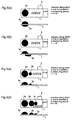
- Figures 3(a) and 3(b) are plan views and side views illustrating check chips having circular convex shaped structural characterizing portions on both surfaces of the sensor body according to the first embodiment of the present invention.
- Figure 3(a) illustrates that placement locations of the respective structural characterizing portions on both surfaces correspond to each other
- figure 3(b) illustrates that the placement locations of the respective structural characterizing portions do not correspond to each other.
- reference numeral 3a designates a structural characterizing portion placed on the upside of the sensor body 1
- reference numeral 3b designates a structural characterizing portion placed on the downside of the sensor body 1.
- the same reference numerals and characters as those in figure 1 designate the same or corresponding parts. So, the descriptions will be omitted.
- the structural characterizing portion 3 of the correction chip shown in figure 1 is provided only on the upside of the sensor body 1.
- the circular convex shaped structural characterizing portions 3a and 3b of are provided on both sides of the sensor body 1, as shown in figure 3.
- placement location of the structural characterizing portion 3 of the check chip is made to be different from the placement location of the structural characterizing portion 3 of the correction chip, thereby the both chips can be distinguished from each other not only from their appearances but also their touch.
- the respective locations of the structural characterizing portions 3a and 3b which are provided on both sides of the sensor body 1 may correspond to each other as shown in figure 3(a), or the respective locations are different from each other as shown in figure 3(b).
- the check chip may have the structural characterizing portions 3 on the both sides of the sensor body 1 and the correction chip may have the same only on upside of the sensor body 1 as described above, or the contrary case (not shown) may be accepted.
- the check chip it is more desirable in the manufacturing that the check chip have the structural characterizing portions 3a and 3b on both sides of the sensor body 1.
- the difference between the check chip and the correction chip may resides in the number of the structural characterizing portions 3, as shown in figure 1 to 4.
- Figures 4(a) and 4(b) are plan views and side views illustrating check chips having plural circular convex shaped structural characterizing portions according to the first embodiment of the present invention.
- Figure 4(a) illustrates that a check chip having two structural characterizing portions on the upside of the sensor body 1
- figure 4(b) illustrates that a check chip having three structural characterizing portions.
- reference numerals 3a, 3b and 3c designate structural characterizing portions which are provided with adjacent to each other on the upside of the sensor body 1, and the same reference numerals and characters as those in figure 1 designate the same or corresponding parts. So, the descriptions will be omitted.
- the structural characterizing portion 3 of the correction chip shown in figure 1 is provided only one on the upside of the sensor body 1.
- the circular convex shaped structural characterizing portions 3a and 3b are provided with adjacent to each other on the upside of the sensor body 1, as shown in figure 4(a).
- the number of the structural characterizing portions 3a and 3b are made to be different from the number of the structural characterizing portion 3 of the correction chip, whereby the both chips can be distinguished from each other not only from their appearances but also from their touch.
- the number of the structural characterizing portions may be provided with either two as shown in figure 4(a) or three as shown in figure 4(b), if the structural characterizing portions can be constituted on the sensor body 1.
- the number of the structural characterizing portions 3 of the check chip may be larger than that of the structural characterizing portion 3 of the correction chip as described above, or the contrary case (not shown) can be accepted.
- the respective sizes of the plural structural characterizing portions 3 of the check chip may be all the same, or there may be some differences between the structural characterizing portions 3a, 3b and 3c as shown in figures 4(a) and 4(b).
- the structural characterizing portions 3a containing a resistor is enlarged and other structural characterizing portions 3b and 3c are diminished, as shown in figure 4(b).
- a part of the plural circular convex shaped structural characterizing portions 3 described with reference to figure 4 may be optical penetrability, as shown in figure 5.
- Figure 5 is a plane view and a side illustrating a check chip, in which a part of the plural circular convex shaped structural characterizing portions is optical penetrability, according to the first embodiment of the present invention.
- reference numeral 3d designates a circular convex shaped structural characterizing portion having optical penetrability.
- Thesame reference numerals and characters as those in figure 4 designate the same or corresponding parts. So, the descriptions will be omitted.
- the sensor and measuring device employed in this first embodiment are often used by a person having good sight, and a person having good sight frequently assists a visually handicapped person in using a sensor measuring device. Therefore, many chips are printed on their surfaces with attention attracting characters for indicating what the chip is used for, such as "for checking” or "CHECK", so as to indicate that the chips are check chips. In this case, when the check chip is provided with a structural characterizing portion 3 which is different from that of the correction chip, reading of the attention attracting character might be interrupted, especially in the case where the number of the structural characterizing portion 3 is large.
- one structural characterizing portion 3d out of the structural characterizing portions 3a and 3d is constituted to have optical penetrability as shown in figure 5, whereby the attention attracting character can be read out even if the attention attracting character printed on the sensor body 1 is hidden under the structural characterizing portion 3.
- check chip may reside in the shape of the structural characterizing portion 3, as shown in figures 1 and 6.
- Figures 6(a) and 6(b) are plane views and side views of check chips in which the shape of convex shaped structural characterizing portions is different from that of the structural characterizing portion of the correction chip, according to the first embodiment of the present invention.
- Figure 6(a) is a view illustrating that the shape of a structural characterizing portion is rectangular convex shaped
- figure 6(b) is a view illustrating that the shape of a structural characterizing portion is circular convex shaped with acute projection.
- the same reference numerals and characters as those in figure 1 designate the same or corresponding parts. So, the descriptions will be omitted.
- the structural characterizing portion 3 of the correction chip shown in figure 1 has a circular convex shaped and gentle dome liked shape.
- the structural characterizing portion 3 of the check chip according to this first embodiment the shape, for example, have circular convex shape with the acute projection, as shown in figure 6(b). Therefore, the shape of the structural characterizing portion 3 of the check chip is made to be different from that of the structural characterizing portion 3 of the correction chip, and the user can distinguish the check chip from the correction chip not only by their appearances but also by their touch.
- the check chip of the first embodiment may a structural characterizing portion 3 which is constituted by combining the shapes of the structural characterizing portions 3 described with reference to figures 2 to 5.
- a structural characterizing portion 3 which is constituted by combining the shapes of the structural characterizing portions 3 described with reference to figures 2 to 5.
- desirable combination can be obtained such that plural structural characterizing portions 3 provided on the upside of the sensor body 1 shaped in triangular or rectangular, the structural characterizing portions 3 provided on both sides of the sensor body 1 are shaped in triangular or square, or a correction chip has a convex shaped portion, in contrast to that a check chip has a concave shaped portion.
- resin is employed for insulation in the structural characterizing portion 3.
- the epoxy type resin is desirable.
- the diameter has a size which is not larger than a width of the sensor body 1. Since the both chips are made to be correspondent to the measuring sensor in the shape, in the case of a chip having approximate 6mm width, for example, it is desirable that a diameter of the approximate circular shaped structural characterizing portion 3 is smaller than 6mm in its maximum. Further, the minimum value of the diameter is not especially limited, though, it is desirable that the diameter is 1mm or more because a resistor is to be buried in the structural characterizing portion 3. When smaller resistor is employed, the structural characterizing portion 3 can be more diminished. However, a size, with which a visually handicapped user can distinguish whether a sensor is a correction sensor or a check sensor from the touch, is required.
- a general forming method for the structural characterizing portion 3 containing a resistor employs conventional printing technique. More particularly, the structural characterizing portion 3 is piled up on the resistor with adjusting the thickness of a masking base material and the viscosity of the resin, via the masking material with a penetration hole of a desirable diameter.
- a check chip which is similar to the correction chip in the shape is manufactured employing the applied printing technique, and then the structural characterizing portions 3b containing no resistor is manually formed, using a syringe full of the resin and a injection needle, thereby producing the check chip shown in figure 4(a).
- the structural characterizing portion 3 of the correction sensor is different from that of the check sensor in the shape, and further, the difference in the shape of the structural characterizing portion 3 is formed so as to be identified by a user from the touch, therefore even a visually handicapped user can easily distinguish the correction chip from the check chip, so as to prevent the user from using the two chips with confused.
- the check chip for a sensor device of the present invention is extremely useful as the one which can be easily distinguished even by a visually handicapped user from a correction chip having similar shape to the check chip, which the correction chip is used for correcting at the time of lot change of a sensor.
Landscapes
- Health & Medical Sciences (AREA)
- Life Sciences & Earth Sciences (AREA)
- Chemical & Material Sciences (AREA)
- General Physics & Mathematics (AREA)
- Physics & Mathematics (AREA)
- Immunology (AREA)
- Pathology (AREA)
- Biochemistry (AREA)
- General Health & Medical Sciences (AREA)
- Analytical Chemistry (AREA)
- Engineering & Computer Science (AREA)
- Molecular Biology (AREA)
- Biomedical Technology (AREA)
- Hematology (AREA)
- Quality & Reliability (AREA)
- Urology & Nephrology (AREA)
- Food Science & Technology (AREA)
- Medicinal Chemistry (AREA)
- Measurement Of The Respiration, Hearing Ability, Form, And Blood Characteristics Of Living Organisms (AREA)
- Measurement Of Length, Angles, Or The Like Using Electric Or Magnetic Means (AREA)
- Credit Cards Or The Like (AREA)
- Corsets Or Brassieres (AREA)
Abstract
Description
Claims (11)
- A check chip which is mounted on a measuring device employing an exclusively used sensor, and checks operations of the measuring device itself, wherein
the check chip is provided thereon with at least one structural characterizing portion which makes a user of the measuring device recognize differences from a correction chip for correcting errors that occur with lot changes in the exclusively used sensor. - The check chip of Claim 1, wherein
the structural characterizing portion has a shape, such as a convex shape, which can be recognized by the user from the touch, and is provided in a location by which the user is considered to pick up the check chip. - The check chip of Claim 1 or Claim 2, wherein a difference between the check chip and the correction chip resides in the size of the structural characterizing portion, when the correction chip has the structural characterizing portion.
- The check chip of Claim 3, wherein
the size of the structural characterizing portion provided on the check chip is larger than that of the structural characterizing portion provided on the correction chip. - The check chip of Claim 3, wherein
the size of the structural characterizing portion provided on the check chip is smaller than that of the structural characterizing portion provided on the correction chip. - The check chip of any of Claims 1 to 5, wherein
the check chip is provided with the structural characterizing portion on the both sides of the check chip. - The check chip of any of Claims 1 to 6, wherein a difference between the check chip and the correction chip resides in the number of the structural characterizing portions.
- The check chip of Claim 7, wherein
the number of the structural characterizing portions provided on the check chip is larger than that of the structural characterizing portions provided on the correction chip. - The check chip of Claim 7, wherein
the number of the structural characterizing portions provided on the check chip is smaller than that of the structural characterizing portions provided on the correction chip. - The check chip of Claim 8, wherein
structural characterizing portion on an attention attracting character printed on an upside of the check chip, among plural structural characterizing portions provided on the check chip, has optical penetrability. - The check chip of any of Claims 1 to 10, wherein a difference between the check chip and the correction chip reside in the shape of the structural characterizing portion.
Applications Claiming Priority (3)
| Application Number | Priority Date | Filing Date | Title |
|---|---|---|---|
| JP2000041716 | 2000-02-18 | ||
| JP2000041716 | 2000-02-18 | ||
| PCT/JP2001/001152 WO2001061342A1 (en) | 2000-02-18 | 2001-02-19 | Inspection chip for sensor measuring instrument |
Publications (2)
| Publication Number | Publication Date |
|---|---|
| EP1172653A1 true EP1172653A1 (en) | 2002-01-16 |
| EP1172653A4 EP1172653A4 (en) | 2003-07-16 |
Family
ID=18564907
Family Applications (1)
| Application Number | Title | Priority Date | Filing Date |
|---|---|---|---|
| EP01904531A Ceased EP1172653A4 (en) | 2000-02-18 | 2001-02-19 | CONTROL CHIP FOR SENSOR MEASURING INSTRUMENT |
Country Status (4)
| Country | Link |
|---|---|
| US (2) | US6792791B2 (en) |
| EP (1) | EP1172653A4 (en) |
| CN (1) | CN1161075C (en) |
| WO (1) | WO2001061342A1 (en) |
Cited By (2)
| Publication number | Priority date | Publication date | Assignee | Title |
|---|---|---|---|---|
| US4818373A (en) * | 1984-10-19 | 1989-04-04 | Engelhard Corporation | Process for upgrading tar and bitumen |
| US6792791B2 (en) * | 2000-02-18 | 2004-09-21 | Matsushita Electric Industrial Co., Ltd. | Inspection chip for sensor measuring instrument |
Families Citing this family (87)
| Publication number | Priority date | Publication date | Assignee | Title |
|---|---|---|---|---|
| US6036924A (en) | 1997-12-04 | 2000-03-14 | Hewlett-Packard Company | Cassette of lancet cartridges for sampling blood |
| US8071384B2 (en) | 1997-12-22 | 2011-12-06 | Roche Diagnostics Operations, Inc. | Control and calibration solutions and methods for their use |
| US6391005B1 (en) | 1998-03-30 | 2002-05-21 | Agilent Technologies, Inc. | Apparatus and method for penetration with shaft having a sensor for sensing penetration depth |
| US8641644B2 (en) | 2000-11-21 | 2014-02-04 | Sanofi-Aventis Deutschland Gmbh | Blood testing apparatus having a rotatable cartridge with multiple lancing elements and testing means |
| US9226699B2 (en) | 2002-04-19 | 2016-01-05 | Sanofi-Aventis Deutschland Gmbh | Body fluid sampling module with a continuous compression tissue interface surface |
| US7682318B2 (en) | 2001-06-12 | 2010-03-23 | Pelikan Technologies, Inc. | Blood sampling apparatus and method |
| WO2002100460A2 (en) | 2001-06-12 | 2002-12-19 | Pelikan Technologies, Inc. | Electric lancet actuator |
| US7041068B2 (en) | 2001-06-12 | 2006-05-09 | Pelikan Technologies, Inc. | Sampling module device and method |
| CA2448902C (en) | 2001-06-12 | 2010-09-07 | Pelikan Technologies, Inc. | Self optimizing lancing device with adaptation means to temporal variations in cutaneous properties |
| WO2002100461A2 (en) | 2001-06-12 | 2002-12-19 | Pelikan Technologies, Inc. | Method and apparatus for improving success rate of blood yield from a fingerstick |
| US7537571B2 (en) | 2001-06-12 | 2009-05-26 | Pelikan Technologies, Inc. | Integrated blood sampling analysis system with multi-use sampling module |
| AU2002348683A1 (en) | 2001-06-12 | 2002-12-23 | Pelikan Technologies, Inc. | Method and apparatus for lancet launching device integrated onto a blood-sampling cartridge |
| US7981056B2 (en) | 2002-04-19 | 2011-07-19 | Pelikan Technologies, Inc. | Methods and apparatus for lancet actuation |
| US8337419B2 (en) | 2002-04-19 | 2012-12-25 | Sanofi-Aventis Deutschland Gmbh | Tissue penetration device |
| US7344507B2 (en) | 2002-04-19 | 2008-03-18 | Pelikan Technologies, Inc. | Method and apparatus for lancet actuation |
| US9795747B2 (en) | 2010-06-02 | 2017-10-24 | Sanofi-Aventis Deutschland Gmbh | Methods and apparatus for lancet actuation |
| US9427532B2 (en) | 2001-06-12 | 2016-08-30 | Sanofi-Aventis Deutschland Gmbh | Tissue penetration device |
| US7344894B2 (en) | 2001-10-16 | 2008-03-18 | Agilent Technologies, Inc. | Thermal regulation of fluidic samples within a diagnostic cartridge |
| US7244265B2 (en) | 2002-04-19 | 2007-07-17 | Pelikan Technologies, Inc. | Method and apparatus for penetrating tissue |
| US7524293B2 (en) | 2002-04-19 | 2009-04-28 | Pelikan Technologies, Inc. | Method and apparatus for penetrating tissue |
| US8784335B2 (en) | 2002-04-19 | 2014-07-22 | Sanofi-Aventis Deutschland Gmbh | Body fluid sampling device with a capacitive sensor |
| US7892185B2 (en) | 2002-04-19 | 2011-02-22 | Pelikan Technologies, Inc. | Method and apparatus for body fluid sampling and analyte sensing |
| US7297122B2 (en) | 2002-04-19 | 2007-11-20 | Pelikan Technologies, Inc. | Method and apparatus for penetrating tissue |
| US7563232B2 (en) | 2002-04-19 | 2009-07-21 | Pelikan Technologies, Inc. | Method and apparatus for penetrating tissue |
| AU2003231749A1 (en) | 2002-04-19 | 2003-11-03 | Pelikan Technologies, Inc. | Device and method for variable speed lancet |
| US7371247B2 (en) | 2002-04-19 | 2008-05-13 | Pelikan Technologies, Inc | Method and apparatus for penetrating tissue |
| US9248267B2 (en) | 2002-04-19 | 2016-02-02 | Sanofi-Aventis Deustchland Gmbh | Tissue penetration device |
| US7909778B2 (en) | 2002-04-19 | 2011-03-22 | Pelikan Technologies, Inc. | Method and apparatus for penetrating tissue |
| US7976476B2 (en) | 2002-04-19 | 2011-07-12 | Pelikan Technologies, Inc. | Device and method for variable speed lancet |
| US8221334B2 (en) | 2002-04-19 | 2012-07-17 | Sanofi-Aventis Deutschland Gmbh | Method and apparatus for penetrating tissue |
| US8702624B2 (en) | 2006-09-29 | 2014-04-22 | Sanofi-Aventis Deutschland Gmbh | Analyte measurement device with a single shot actuator |
| US8267870B2 (en) | 2002-04-19 | 2012-09-18 | Sanofi-Aventis Deutschland Gmbh | Method and apparatus for body fluid sampling with hybrid actuation |
| US7141058B2 (en) | 2002-04-19 | 2006-11-28 | Pelikan Technologies, Inc. | Method and apparatus for a body fluid sampling device using illumination |
| US9795334B2 (en) | 2002-04-19 | 2017-10-24 | Sanofi-Aventis Deutschland Gmbh | Method and apparatus for penetrating tissue |
| US7410468B2 (en) | 2002-04-19 | 2008-08-12 | Pelikan Technologies, Inc. | Method and apparatus for penetrating tissue |
| US8579831B2 (en) | 2002-04-19 | 2013-11-12 | Sanofi-Aventis Deutschland Gmbh | Method and apparatus for penetrating tissue |
| US7892183B2 (en) | 2002-04-19 | 2011-02-22 | Pelikan Technologies, Inc. | Method and apparatus for body fluid sampling and analyte sensing |
| US7291117B2 (en) | 2002-04-19 | 2007-11-06 | Pelikan Technologies, Inc. | Method and apparatus for penetrating tissue |
| US7232451B2 (en) | 2002-04-19 | 2007-06-19 | Pelikan Technologies, Inc. | Method and apparatus for penetrating tissue |
| US7331931B2 (en) | 2002-04-19 | 2008-02-19 | Pelikan Technologies, Inc. | Method and apparatus for penetrating tissue |
| US7901362B2 (en) | 2002-04-19 | 2011-03-08 | Pelikan Technologies, Inc. | Method and apparatus for penetrating tissue |
| US7226461B2 (en) | 2002-04-19 | 2007-06-05 | Pelikan Technologies, Inc. | Method and apparatus for a multi-use body fluid sampling device with sterility barrier release |
| US7648468B2 (en) | 2002-04-19 | 2010-01-19 | Pelikon Technologies, Inc. | Method and apparatus for penetrating tissue |
| US7717863B2 (en) | 2002-04-19 | 2010-05-18 | Pelikan Technologies, Inc. | Method and apparatus for penetrating tissue |
| US7485128B2 (en) | 2002-04-19 | 2009-02-03 | Pelikan Technologies, Inc. | Method and apparatus for penetrating tissue |
| US8360992B2 (en) | 2002-04-19 | 2013-01-29 | Sanofi-Aventis Deutschland Gmbh | Method and apparatus for penetrating tissue |
| US7674232B2 (en) | 2002-04-19 | 2010-03-09 | Pelikan Technologies, Inc. | Method and apparatus for penetrating tissue |
| US7491178B2 (en) | 2002-04-19 | 2009-02-17 | Pelikan Technologies, Inc. | Method and apparatus for penetrating tissue |
| US7374544B2 (en) | 2002-04-19 | 2008-05-20 | Pelikan Technologies, Inc. | Method and apparatus for penetrating tissue |
| US7547287B2 (en) | 2002-04-19 | 2009-06-16 | Pelikan Technologies, Inc. | Method and apparatus for penetrating tissue |
| US7229458B2 (en) | 2002-04-19 | 2007-06-12 | Pelikan Technologies, Inc. | Method and apparatus for penetrating tissue |
| US9314194B2 (en) | 2002-04-19 | 2016-04-19 | Sanofi-Aventis Deutschland Gmbh | Tissue penetration device |
| US8574895B2 (en) | 2002-12-30 | 2013-11-05 | Sanofi-Aventis Deutschland Gmbh | Method and apparatus using optical techniques to measure analyte levels |
| EP1593961B1 (en) * | 2003-02-14 | 2013-01-09 | Arkray Inc. | Analyzing tool with knob part |
| EP2238892A3 (en) | 2003-05-30 | 2011-02-09 | Pelikan Technologies Inc. | Apparatus for body fluid sampling |
| ES2490740T3 (en) | 2003-06-06 | 2014-09-04 | Sanofi-Aventis Deutschland Gmbh | Apparatus for blood fluid sampling and analyte detection |
| WO2006001797A1 (en) | 2004-06-14 | 2006-01-05 | Pelikan Technologies, Inc. | Low pain penetrating |
| US7604592B2 (en) | 2003-06-13 | 2009-10-20 | Pelikan Technologies, Inc. | Method and apparatus for a point of care device |
| US7452457B2 (en) | 2003-06-20 | 2008-11-18 | Roche Diagnostics Operations, Inc. | System and method for analyte measurement using dose sufficiency electrodes |
| HUE039852T2 (en) * | 2003-06-20 | 2019-02-28 | Hoffmann La Roche | Method and reagent for producing narrow, homogenous reagent strips |
| US8058077B2 (en) | 2003-06-20 | 2011-11-15 | Roche Diagnostics Operations, Inc. | Method for coding information on a biosensor test strip |
| US7645373B2 (en) | 2003-06-20 | 2010-01-12 | Roche Diagnostic Operations, Inc. | System and method for coding information on a biosensor test strip |
| US7604721B2 (en) | 2003-06-20 | 2009-10-20 | Roche Diagnostics Operations, Inc. | System and method for coding information on a biosensor test strip |
| US7718439B2 (en) | 2003-06-20 | 2010-05-18 | Roche Diagnostics Operations, Inc. | System and method for coding information on a biosensor test strip |
| US7645421B2 (en) | 2003-06-20 | 2010-01-12 | Roche Diagnostics Operations, Inc. | System and method for coding information on a biosensor test strip |
| US7597793B2 (en) | 2003-06-20 | 2009-10-06 | Roche Operations Ltd. | System and method for analyte measurement employing maximum dosing time delay |
| US8206565B2 (en) | 2003-06-20 | 2012-06-26 | Roche Diagnostics Operation, Inc. | System and method for coding information on a biosensor test strip |
| US8148164B2 (en) | 2003-06-20 | 2012-04-03 | Roche Diagnostics Operations, Inc. | System and method for determining the concentration of an analyte in a sample fluid |
| EP1671096A4 (en) | 2003-09-29 | 2009-09-16 | Pelikan Technologies Inc | METHOD AND APPARATUS FOR AN IMPROVED SAMPLING INTERFERENCE DEVICE |
| EP1680014A4 (en) | 2003-10-14 | 2009-01-21 | Pelikan Technologies Inc | METHOD AND APPARATUS PROVIDING A VARIABLE USER INTERFACE |
| US7822454B1 (en) | 2005-01-03 | 2010-10-26 | Pelikan Technologies, Inc. | Fluid sampling device with improved analyte detecting member configuration |
| WO2005065414A2 (en) | 2003-12-31 | 2005-07-21 | Pelikan Technologies, Inc. | Method and apparatus for improving fluidic flow and sample capture |
| US8828203B2 (en) | 2004-05-20 | 2014-09-09 | Sanofi-Aventis Deutschland Gmbh | Printable hydrogels for biosensors |
| US9775553B2 (en) | 2004-06-03 | 2017-10-03 | Sanofi-Aventis Deutschland Gmbh | Method and apparatus for a fluid sampling device |
| EP1765194A4 (en) | 2004-06-03 | 2010-09-29 | Pelikan Technologies Inc | METHOD AND APPARATUS FOR MANUFACTURING A DEVICE FOR SAMPLING LIQUIDS |
| US7556723B2 (en) | 2004-06-18 | 2009-07-07 | Roche Diagnostics Operations, Inc. | Electrode design for biosensor |
| US7569126B2 (en) | 2004-06-18 | 2009-08-04 | Roche Diagnostics Operations, Inc. | System and method for quality assurance of a biosensor test strip |
| US8652831B2 (en) | 2004-12-30 | 2014-02-18 | Sanofi-Aventis Deutschland Gmbh | Method and apparatus for analyte measurement test time |
| JP5027819B2 (en) * | 2006-11-30 | 2012-09-19 | パナソニック株式会社 | Blood test equipment |
| CN101715555A (en) * | 2007-04-27 | 2010-05-26 | 艾伯特糖尿病护理公司 | Test strip identification using conductive patterns |
| US20080274552A1 (en) * | 2007-05-04 | 2008-11-06 | Brian Guthrie | Dynamic Information Transfer |
| JP2009115518A (en) * | 2007-11-02 | 2009-05-28 | Sumitomo Electric Ind Ltd | Biosensor |
| EP2265324B1 (en) | 2008-04-11 | 2015-01-28 | Sanofi-Aventis Deutschland GmbH | Integrated analyte measurement system |
| US9375169B2 (en) | 2009-01-30 | 2016-06-28 | Sanofi-Aventis Deutschland Gmbh | Cam drive for managing disposable penetrating member actions with a single motor and motor and control system |
| JP2010181219A (en) * | 2009-02-04 | 2010-08-19 | Panasonic Corp | Measuring device, inspecting sensor used therein, and method of inspecting measuring device |
| US8965476B2 (en) | 2010-04-16 | 2015-02-24 | Sanofi-Aventis Deutschland Gmbh | Tissue penetration device |
| KR20120071921A (en) * | 2010-12-23 | 2012-07-03 | 한국전자통신연구원 | Composition for filling through silicon vias (tsvs), tsv filling method and substrate including tsv filling formed of the composition |
Family Cites Families (23)
| Publication number | Priority date | Publication date | Assignee | Title |
|---|---|---|---|---|
| US3783345A (en) * | 1971-09-08 | 1974-01-01 | Graham White Mfg Co | Heat-dissipating encapsulated semi-conductor assembly |
| US4308085A (en) * | 1980-07-28 | 1981-12-29 | Jenoptik Jena Gmbh | Process for the preparation of high molecular thermoplastic epoxide-amine-polyadducts |
| US4366241A (en) * | 1980-08-07 | 1982-12-28 | Syva Company | Concentrating zone method in heterogeneous immunoassays |
| JPS584981A (en) | 1982-06-28 | 1983-01-12 | Nec Corp | Semiconductor device |
| GB8413830D0 (en) | 1984-05-31 | 1984-07-04 | Seltronix Ltd | Blood glucose monitor |
| JPH0648256B2 (en) | 1985-06-21 | 1994-06-22 | 松下電器産業株式会社 | Biosensor |
| US6066847A (en) * | 1989-01-19 | 2000-05-23 | Futrex Inc. | Procedure for verifying the accuracy of non-invasive blood glucose measurement instruments |
| JPH0820412B2 (en) | 1990-07-20 | 1996-03-04 | 松下電器産業株式会社 | Quantitative analysis method and device using disposable sensor |
| JP3045761B2 (en) * | 1990-11-14 | 2000-05-29 | 株式会社京都第一科学 | Color test paper with correction paper strip |
| JPH04188065A (en) | 1990-11-21 | 1992-07-06 | Kyoto Daiichi Kagaku:Kk | Tool and method for analyzing liquid sample |
| WO1992015859A1 (en) * | 1991-02-27 | 1992-09-17 | Boehringer Mannheim Corporation | Apparatus and method for analyzing body fluids |
| ES2153335T3 (en) * | 1993-06-08 | 2006-09-01 | Roche Diagnostics Operations, Inc. | BIOSENSOR METER THAT DETECTS THE PROPER ADJUSTMENT OF THE ELECTRODES AND DISTINGUISHES SAMPLING STRIPS AND CHECKING STRIPS. |
| JPH0820412A (en) | 1994-07-05 | 1996-01-23 | Daifuku Co Ltd | Controller of rotary rack |
| US5526120A (en) * | 1994-09-08 | 1996-06-11 | Lifescan, Inc. | Test strip with an asymmetrical end insuring correct insertion for measuring |
| AU6904496A (en) * | 1995-08-22 | 1997-03-19 | Andcare, Inc. | Handheld electromonitor device |
| US5962215A (en) * | 1996-04-05 | 1999-10-05 | Mercury Diagnostics, Inc. | Methods for testing the concentration of an analyte in a body fluid |
| DE19781162C2 (en) | 1996-10-30 | 2002-05-23 | Mercury Diagnostics Inc | Test strips for the analysis of a body fluid sample and for evaluation in a test instrument |
| SE9604053D0 (en) | 1996-11-05 | 1996-11-05 | Alfa Laval Agri Ab | Teat rubber and process for the manufacture of a teat rubber |
| DE29720299U1 (en) * | 1997-11-15 | 1998-01-15 | Held, Fred, 22299 Hamburg | Test strips for determining blood sugar |
| US6009632A (en) * | 1997-12-12 | 2000-01-04 | Mercury Diagnostics, Inc. | Alignment system for optical analyte testing meter components |
| US5995236A (en) * | 1998-04-13 | 1999-11-30 | Mit Development Corporation | Blood fluid characteristics analysis instrument |
| AU768312B2 (en) * | 1998-11-30 | 2003-12-11 | Abbott Laboratories | Analyte test instrument having improved calibration and communication processes |
| CN1161075C (en) * | 2000-02-18 | 2004-08-11 | 松下电器产业株式会社 | Inspection sheets for sensor measurement devices |
-
2001
- 2001-02-19 CN CNB018002625A patent/CN1161075C/en not_active Expired - Lifetime
- 2001-02-19 EP EP01904531A patent/EP1172653A4/en not_active Ceased
- 2001-02-19 WO PCT/JP2001/001152 patent/WO2001061342A1/en not_active Ceased
- 2001-02-19 US US09/958,886 patent/US6792791B2/en not_active Expired - Lifetime
-
2003
- 2003-10-20 US US10/687,757 patent/US20040079135A1/en not_active Abandoned
Cited By (2)
| Publication number | Priority date | Publication date | Assignee | Title |
|---|---|---|---|---|
| US4818373A (en) * | 1984-10-19 | 1989-04-04 | Engelhard Corporation | Process for upgrading tar and bitumen |
| US6792791B2 (en) * | 2000-02-18 | 2004-09-21 | Matsushita Electric Industrial Co., Ltd. | Inspection chip for sensor measuring instrument |
Also Published As
| Publication number | Publication date |
|---|---|
| EP1172653A4 (en) | 2003-07-16 |
| WO2001061342A1 (en) | 2001-08-23 |
| US20040079135A1 (en) | 2004-04-29 |
| CN1363038A (en) | 2002-08-07 |
| CN1161075C (en) | 2004-08-11 |
| US20020152793A1 (en) | 2002-10-24 |
| US6792791B2 (en) | 2004-09-21 |
Similar Documents
| Publication | Publication Date | Title |
|---|---|---|
| US6792791B2 (en) | Inspection chip for sensor measuring instrument | |
| JP5091239B2 (en) | Calibration data transfer system and method | |
| US8236166B2 (en) | No calibration analyte sensors and methods | |
| US20090214384A1 (en) | Identification of a strip type by the meter using conductive patterns on the strip | |
| EP1275732B1 (en) | Electrochemical test sensor with an underfill detection system | |
| US7918121B2 (en) | Meter system designed to run singulated test sensors | |
| EP1054805B1 (en) | Capillary fill device with improved fluid delivery | |
| JP2007522449A (en) | System and method for detecting blood glucose | |
| EP2833132B1 (en) | Kit comprising a detection instrument and a biosensor with automatic coding device | |
| US7678261B2 (en) | Apparatus and method for measuring reaction result of samples on biosensor | |
| EP1275963B1 (en) | Volume meter testing device | |
| JP4184573B2 (en) | Biosensor | |
| US20080169799A1 (en) | Method for biosensor analysis | |
| JPWO2001061342A1 (en) | Inspection chip for sensor measuring device |
Legal Events
| Date | Code | Title | Description |
|---|---|---|---|
| PUAI | Public reference made under article 153(3) epc to a published international application that has entered the european phase |
Free format text: ORIGINAL CODE: 0009012 |
|
| 17P | Request for examination filed |
Effective date: 20011106 |
|
| AK | Designated contracting states |
Kind code of ref document: A1 Designated state(s): AT BE CH CY DE DK ES FI FR GB GR IE IT LI LU MC NL PT SE TR |
|
| A4 | Supplementary search report drawn up and despatched |
Effective date: 20030604 |
|
| RIC1 | Information provided on ipc code assigned before grant |
Ipc: 7A 61B 5/00 B Ipc: 7G 01N 33/487 B Ipc: 7G 01N 33/48 A |
|
| RBV | Designated contracting states (corrected) |
Designated state(s): DE FR GB IT |
|
| 17Q | First examination report despatched |
Effective date: 20071213 |
|
| RAP1 | Party data changed (applicant data changed or rights of an application transferred) |
Owner name: ARKRAY, INC. Owner name: PANASONIC CORPORATION |
|
| STAA | Information on the status of an ep patent application or granted ep patent |
Free format text: STATUS: THE APPLICATION HAS BEEN REFUSED |
|
| 18R | Application refused |
Effective date: 20101027 |