EP1171994B1 - Method and apparatus to extend dynamic range of time delay and integrate charge coupled devices - Google Patents
Method and apparatus to extend dynamic range of time delay and integrate charge coupled devices Download PDFInfo
- Publication number
- EP1171994B1 EP1171994B1 EP00918227A EP00918227A EP1171994B1 EP 1171994 B1 EP1171994 B1 EP 1171994B1 EP 00918227 A EP00918227 A EP 00918227A EP 00918227 A EP00918227 A EP 00918227A EP 1171994 B1 EP1171994 B1 EP 1171994B1
- Authority
- EP
- European Patent Office
- Prior art keywords
- charge
- barrier
- channel
- stage
- recited
- Prior art date
- Legal status (The legal status is an assumption and is not a legal conclusion. Google has not performed a legal analysis and makes no representation as to the accuracy of the status listed.)
- Expired - Lifetime
Links
Images


Classifications
-
- H—ELECTRICITY
- H10—SEMICONDUCTOR DEVICES; ELECTRIC SOLID-STATE DEVICES NOT OTHERWISE PROVIDED FOR
- H10F—INORGANIC SEMICONDUCTOR DEVICES SENSITIVE TO INFRARED RADIATION, LIGHT, ELECTROMAGNETIC RADIATION OF SHORTER WAVELENGTH OR CORPUSCULAR RADIATION
- H10F39/00—Integrated devices, or assemblies of multiple devices, comprising at least one element covered by group H10F30/00, e.g. radiation detectors comprising photodiode arrays
- H10F39/10—Integrated devices
- H10F39/12—Image sensors
- H10F39/15—Charge-coupled device [CCD] image sensors
- H10F39/153—Two-dimensional or three-dimensional array CCD image sensors
- H10F39/1538—Time-delay and integration
-
- H—ELECTRICITY
- H04—ELECTRIC COMMUNICATION TECHNIQUE
- H04N—PICTORIAL COMMUNICATION, e.g. TELEVISION
- H04N25/00—Circuitry of solid-state image sensors [SSIS]; Control thereof
- H04N25/50—Control of the SSIS exposure
- H04N25/57—Control of the dynamic range
- H04N25/571—Control of the dynamic range involving a non-linear response
- H04N25/575—Control of the dynamic range involving a non-linear response with a response composed of multiple slopes
-
- H—ELECTRICITY
- H04—ELECTRIC COMMUNICATION TECHNIQUE
- H04N—PICTORIAL COMMUNICATION, e.g. TELEVISION
- H04N25/00—Circuitry of solid-state image sensors [SSIS]; Control thereof
- H04N25/60—Noise processing, e.g. detecting, correcting, reducing or removing noise
- H04N25/62—Detection or reduction of noise due to excess charges produced by the exposure, e.g. smear, blooming, ghost image, crosstalk or leakage between pixels
- H04N25/621—Detection or reduction of noise due to excess charges produced by the exposure, e.g. smear, blooming, ghost image, crosstalk or leakage between pixels for the control of blooming
- H04N25/622—Detection or reduction of noise due to excess charges produced by the exposure, e.g. smear, blooming, ghost image, crosstalk or leakage between pixels for the control of blooming by controlling anti-blooming drains
-
- H—ELECTRICITY
- H04—ELECTRIC COMMUNICATION TECHNIQUE
- H04N—PICTORIAL COMMUNICATION, e.g. TELEVISION
- H04N25/00—Circuitry of solid-state image sensors [SSIS]; Control thereof
- H04N25/70—SSIS architectures; Circuits associated therewith
- H04N25/71—Charge-coupled device [CCD] sensors; Charge-transfer registers specially adapted for CCD sensors
- H04N25/711—Time delay and integration [TDI] registers; TDI shift registers
-
- H—ELECTRICITY
- H10—SEMICONDUCTOR DEVICES; ELECTRIC SOLID-STATE DEVICES NOT OTHERWISE PROVIDED FOR
- H10F—INORGANIC SEMICONDUCTOR DEVICES SENSITIVE TO INFRARED RADIATION, LIGHT, ELECTROMAGNETIC RADIATION OF SHORTER WAVELENGTH OR CORPUSCULAR RADIATION
- H10F39/00—Integrated devices, or assemblies of multiple devices, comprising at least one element covered by group H10F30/00, e.g. radiation detectors comprising photodiode arrays
- H10F39/10—Integrated devices
- H10F39/12—Image sensors
- H10F39/15—Charge-coupled device [CCD] image sensors
- H10F39/158—Charge-coupled device [CCD] image sensors having arrangements for blooming suppression
Definitions
- the present invention is related to the field of imaging devices.
- An embodiment of the invention relates to extending the dynamic range of Time Delay and Integrate (TDI) imagers.
- TDI Time Delay and Integrate
- Typical single line imagers for example, Charge Couple Device (CCD) imagers, incorporate a single row of photosensitive electric devices, such as photodetectors, to collect photonic charge.
- a photo-detector converts the collected photonic charge into an electrical charge that is related to the amount of photonic charge collected.
- a Time Delay & Integration (TDI) method of operating CCD imagers incorporates multiple single row CCD scanners in an imaging array. Each row in the array collects image data for a finite period of time as the target image and the imager move relative to each other.
- TDI Time Delay & Integration
- TDI-CCD scanners offer an advantage over single line scanners in that TDI-CCD devices provide for longer times to collect and integrate photonic charge from the target image. The longer collection time also increases the sensitivity of the imager.
- Another method to avoid excess charge-accumulation problems is to reduce the amount of time that is used in collecting an image.
- This method has the disadvantage of reducing sensitivity of the imaging device. Thus, dark images remain relatively dark.
- TDI-CCD devices that allows for the collection of sufficient image data to view dark images while not losing data from relatively bright images.
- US-A-5 114 237 discloses a photosensitive sensor including multilinear arrays of n lines of cells which operate by charge integration and time delay by successive observations of the same image line by the n lines in the array and by accumulation of the corresponding n observations in the cells of the sensor.
- the number of lines between which the charge integration and delays are performed is programmed to be between 1 and n. This programming is performed as a function of the average illumination of the image analysed. To do so, the electrodes of certain lines of cells are used, and potentials are applied to them; either the normal charge transfer potentials or a blocking potential which isolates the lines beyond this blocking electrode from a reading stage.
- a method that increases the intra-scene dynamic range of a TDI-CCD device by selectively limiting the amount of charge collected in each stage by selectively setting blooming barrier levels.
- the maximum accumulated charge collected in each cell is incrementally increased as the charge is passed from one cell to a subsequent cell.
- the level of the barrier is set in a step-wise increasing manner that limits the amount of charge collected in each stage while allowing for the accumulation of progressively greater amounts of collected charge in subsequent cells.
- a step-wise increase in the barrier levels changes the reference level at which charge is accumulated in a cell.
- TDI-CCD array imagers As would be understood the principles of the invention disclosed are related to TDI-CCD array imagers. However, the principles of the invention may also be applied to other solid-state TDI imaging devices, for example, CMOS TDI-APS devices.
- FIG. 1 illustrates an exemplary schematic diagram of an 8-stage TDI-CCD device 100. Only four photosensitive devices (pixel cells) 115, among a plurality of cells in each stage are shown to describe the operation of the TDI-CCD device.
- the photonic charge from a target image is collected beginning in pixel cells 115 associated with the first stage -- i.e., stage 101.
- stage 101 the first stage
- stage 101 the image moves past the pixel cells in a next stage (102).
- the cells in this stage then collect photonic charge from the target image.
- the charge collected in previous cells is added to the charge collected in the currently-imaging cell.
- the charge collected in pixel cell 115 associated with stage 101 is added or transferred to pixel cell 115 associated with stage 102, as the image moves past stage 102.
- the accumulated charge in pixel cell 115 associated with stage 102 is added to the charge collected in pixel cell 115 associated with stage 103, as the image moves past stage 103.
- This transferring of accumulated photonic charge from a cell in one stage to a cell in a subsequent stage continues, one stage at a time, until an end stage is reached -- in this case, stage 108.
- the photonic charge collected for the image is accumulated and integrated over the depth of the TDI-CCD device, -- i.e., stages 101-108.
- the accumulated charge is read out from the TDI-CCD device.
- the charge is transferred along a channel of pixel cells 115, known as a transfer channel, illustrated for one channel of pixel cells as 120.
- a transfer channel illustrated for one channel of pixel cells as 120.
- the excess energy would normally overflow the cell and "spread" into an adjacent cell.
- channels are isolated from one another by blooming drains 125 and barriers 130. The level at which accumulated charge is deemed excessive is determined by barrier 130 that exists between, for example, transfer channel 120 and drain 125.
- barrier 130 The greater the level, or potential, of barrier 130, the greater the amount of accumulated charge that may be collected in each cell 115.
- the levels of barrier 130 are set to achieve the maximum accumulation of charge - i.e., saturation level -- in a pixel cell.
- barrier 130 is positioned horizontally adjacent to channel 120 and 121.
- barrier 130 may also be positioned vertically adjacent to channels 120 and 121 to limit the charge capacity of pixel cell 115.
- Figure 2 illustrates the operation of barrier 130 in controlling excessive charge.
- pixel cell 115 fills to a value that is set by barrier 130.
- the excess as represented by charge 140, is directed into drain 125.
- any further charge that may be collected is simply discarded. The maximum level of barrier 130 thus limits the accumulated charge.
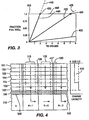
- Figure 3 illustrates an exemplary performance characteristic of TDI-CCD device of Figure 1 for three images of different brightness levels.
- the charge collected by the imager is represented by response characteristic 400.
- each pixel cell 115 in a stage adds a substantially similar amount of charge to pixel cell 115 in the next subsequent stage as the imager and target image move past each other.
- the accumulated charge collected increases proportionally to the number of stages in the imager.
- the total amount of charge collected after the eight stages remains below the barrier level 465 set by barrier 130.
- the charge collected is represented by response characteristic 420.
- the charge of an even brighter image is collected.
- the response to this brighter image is represented by response characteristic 440.
- the brightness of the image causes the accumulated charge to exceed the maximum level set by barrier 130 (at level 465 ) after scanning of the image by only about two of the CCD stages. Were the accumulated charge permitted to accumulate through continuing CCD stages, that charge would be represented by the dashed line portion 445 of response characteristic 440, but the charge is limited by barrier level 465. Barrier level 465 thus limits the response characteristic of the imager. Charge above barrier level 465 is simply discarded into drain 125 and the accumulated charge for this third exemplary image thus remains limited at level 465 as represented by response characteristic 460.
- Figure 4 illustrates an 8-stage TDI-CCD in accordance with the principles of the invention.
- barrier 130 is selectively set in accordance with the capacity charge curve 510. Accordingly, the amount of charge accumulated and retained in each stage is incremental increased.
- barrier 130 is set to limit the accumulated charge to twenty-five per cent (0.25) of maximum barrier level 465 in stages 101-105 of the imager, and fifty percent of that level for stages 106 and 107.
- the level of barrier 130 is set to the maximum barrier level 465.
- the maximum barrier level may be set independently of the maximum capacity of pixel cell 115, but is typically set substantially equal to the maximum capacity of the pixel cell.
- barrier 130 is selectively set in an step-wise pattern that limits the amount of data collected in the early stages of collection while allowing for incrementally greater amounts of charge in latter stages.
- stages 101-105 accumulate 25 percent of the charge that could be collected.
- Stages 106 and 107 accumulate 50 percent of the charge that could be collected, and stage 108 allows for the accumulation of a maximum amount of charge.
- the maximum amount of charge may be collected without causing a saturation of pixel cell 115.
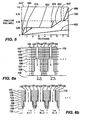
- Figure 5 illustrates the response characteristics of a TDI-CCD device having barrier characteristics selectively set in accordance with the exemplary characteristics illustrated in Figure 4 for the three exemplary images discussed in regard to Figure 3.
- the charge collected is represented by response characteristic 600.
- Response characteristic 600 is similar to the response characteristic 400 of Figure 3, as the accumulated charge does not exceed the selectively set barrier levels of stages 101-105, 106-107 or 108. Accordingly, the response characteristic is not altered and the accumulated charge is not limited.
- the accumulated charge is shown to exceed the first barrier level while charge is collected in stage 102. That is, the accumulation of the charge collected in stage 101 and the charge being collected in stage 102 exceeds the barrier level selectively set for stages 101 through 105. Any additional charge collected in stages 103 through 105 would, accordingly, cause the accumulated charge to exceed the level of barrier 130 and is thus drained off.
- the accumulated charge in stages 103 through 105 remains limited to 25 percent of the charge that may be collected, as represented by response characteristic 620.
- the level of barrier 130 is increased to 50 percent of the maximum barrier level to allow an incremental increase in the charge collected.
- stage 106 As stage 106 moves past the target image, charge is accumulated in pixel cells 115 associated with stage 106. The increase in accumulated charge is represented by response characteristic 630. As shown, the accumulated charge exceeds the level of barrier 130 during the charge collection of stage 107 and the excess charge is drained off. The accumulated charge remains limited to the 50 percent level, as represented by response characteristic 640. At stage 108, the level of barrier 130 is increased to allow an incremental increase in the charge collected. As stage 108 moves past the target image, charge is accumulated, as represented by response characteristic 650. The charge level continues to accumulate until the collected charge is read out in stage 110.
- the accumulated charge level is substantially less than the maximum level; hence, the brightest image data is not lost because the image data is compressed.
- an imager incorporating a step-wise increase in the level of barrier 130 causes alterations or shifts in reference points that are used by subsequent cells to accumulate charge. These alterations in the reference points allow for the collection of more data from brighter images.
- the brightness of the image causes the charge collected to exceed the first level of barrier 130 during the collection phase of stage 101. Any charge collected as the target image moves past stages 101 through 105 is thus drained off.
- the level of the accumulated charge remains fixed at the barrier level as represented by response characteristic 620.
- the level of barrier 130 is increased.
- charge is again accumulated in pixel cell 115 associated with stage 106, as represented by response characteristic 670.
- the brightness of the image causes the accumulated charge to quickly exceed the increased barrier level.
- any charge collected after this increased barrier level is exceeded is drained off.
- the accumulated charge level remains limited during stage 106 and continuing through stage 107, as represented by response characteristic 640.
- the level of barrier 130 is incrementally increased and charge is again accumulated, as represented by the response characteristic 680.
- the brightest portions of the image are collected and the brightest portions of the image are not lost.
- the altered reference points compress the image data to allow pixel cells to accumulate charge that would otherwise be greater than their maximum capability. These alterations in the reference points allow for the collection of image data from brighter images that would otherwise be lost without affecting low light level performance.
- the dynamic range of a TDI-CCD device is extended by selectively setting levels of barriers that limit the charge collection capability.
- the selectively set barrier levels shift the reference point of accumulated charge.
- the altered, or shifted, reference point causes the imager to compress brighter portions of an image while not influencing the lower intensity portions of the same image.
- the scope of the invention is not limited to the step-wise increase in charge capacity in the exemplary 8-stage TDI-CCD device illustrated. Rather the method of setting progressive barrier levels, and thereby progressively accumulating charge in a TDI-CCD device, may also be determined using, for example, exponential, logarithmic, inverse logarithmic, geometric or polynomial functions. Furtherstill, the number of barrier levels also may be increased commensurate with the number of stages in a TDI-CCD device. Thus, the number of different barrier levels may be set substantially equal to the number of stages.
- Figure 6a illustrates one embodiment for fabricating a TDI-CCD imager having a charge capacity illustrated in Figure 4.
- the barrier level 130 is set to limit the amount of charge collected.
- barrier levels are set to limit pixel cell 115 associated with stages 101 through 105 to collect only twenty-five (25) percent of full capacity of pixel cell 115 -- i.e., maximum level 465.
- barrier levels are set to limit pixel cell 115 associated with stages 106 and 107 to collect and retain an accumulated charge that corresponds to fifty (50) percent of full capacity.
- the barrier levels are set to the full width of pixel cell 115 to collect and retain an accumulated charge that is substantially equal to full capacity.
- Figure 6b illustrates a second embodiment for fabricating a TDI-CCD imager having a charge capacity illustrated in Figure 4.
- the barrier levels, or potentials are constant but are positioned to adjust the width of pixel cells 115 to limit the charge collected. In this case, the amount of charge collected is limited by the size of the pixel cells. Further, the width of barrier level 130 remains substantially constant.
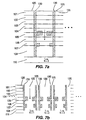
- Figure 7a illustrates a second embodiment of fabricating a TDI-CCD device to achieve the exemplary step-wise accumulated charge characteristics illustrated in Figure 4.
- the pixel cell charge capacity is set in designated stages to limit the accumulated charge.
- the width of pixel 115 in stages 101 through 104 is set at a maximum level 465 -- i.e., full collection capacity.
- the width of pixel 115 is reduced to twenty-five (25) percent of maximum level 465.
- the width of pixel 115 is again increased to maximum level 465, and at stage 107, the width of pixel 115 is reduced to fifty (50) percent of maximum level 465.
- FIG. 108 the width of pixel 115 is again increased to maximum level 465.
- the narrow channel regions at stages 105 and 107 act as charge clippers.
- Figure 7b illustrates another embodiment, similar to that described in regard to Figure 7a, wherein the width of barrier 130 is remains substantially constant. This embodiment is advantageous as the width of drain 125 is correspondingly increased when the size of pixel 115 is decreased. This increase in drain 125 allows for the draining of excessive accumulated charge.
- the depth of the pixel cell 115 may also be used to control pixel charge capacity.
- the depth of pixel cells 115 associated with stages 101-105 may be set to collect twenty-five percent of full charge capacity.
- the depth of pixel cells 115 associated with stages 106-107 may be set to collect fifty percent of full charge capacity and the depth of pixel cell 115 associated with stage 108 may be set to accumulate a full charge.
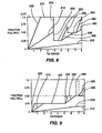
- Figure 8 illustrates the response characteristics of this embodiment of the invention to the three exemplary images discussed in regard to Figure 3 and Figure 5.
- the response characteristic to the first exemplary image is represented by the response characteristic 800.
- the accumulated charge in stages 101 through 108 remains lower than the associated barrier levels.
- the selectively set levels do not influence the response characteristic of the TDI-CCD device to this first exemplary image.
- the charge accumulated in stages 101 through 104 as represented by response 810, rises to maximum level 465.
- the charge capacity of pixel cell 115 is set to twenty-five percent of maximum level 465.
- the accumulated charge above this twenty-five percent level is drained off, as represented by response 820. Furthermore, any additional charge collected during stage 105 is also drained off. Thus, the accumulated charge remains limited, as represented by response characteristic 830.
- the charge capacity of pixel cell 115 is again increased to maximum level 465 and charge is again accumulated, as represented by response characteristic 840.
- the charge capacity of the associated pixel cell 115 is reduced to fifty percent. Any charge collected above this fifty-percent level is, accordingly, drained off and the accumulated charge remains at a fixed level, as is represented by response characteristic 850.
- stage 108 the charge capacity of the associated pixel cell 115 increased to maximum level 465 and charge again is accumulated, as represented by response characteristic 860. Accordingly, the brighter portions of the imager are again captured in the imaging device similar to that illustrated in Figure 5.
- the accumulated charge quickly rises to maximum level 465, as illustrated by response characteristic 865.
- Any additional charge that may be collected in stages 102 - 104 is drained off, as represented by response characteristic 870.
- the charge capacity of the associated pixel cell 115 is set at twenty five percent and any accumulated charge above this level is drained off, as represented by response characteristic 875. Further, any additional charge collected is similarly drained off and the accumulated charge level remains constant, as represented by response characteristic 830.
- the charge capacity of the associated pixel cell 115 is again increased to maximum level 465. The charge is again accumulated, as represented by response characteristic 880.
- the charge capacity of the associated pixel cell 115 is again reduced to fifty percent, and the accumulated charge above this reduced level is again drained off, as represented by response characteristic 885.
- the accumulated charge remains fixed at this level as any additional charge collected is drained off, as represented by response characteristic 850.
- the charge capacity of the associated pixel cell 115 is again increased and the accumulated charge again increases, as represented by response 890.
- the brightest portions of this third exemplary image are thus captured in a manner similar to that illustrated in Figure 5.
- the representation of the transfer channel having varying size is intended merely to illustrate different methods of achieving the exemplary model of varying barrier levels. Other methods may also be used to achieve similar increases in accumulated charge.
- a further means of increasing dynamic range is achieved by placing a filtering element over at least one stage of a TDI-CCD device.
- Filter elements are used to further extend dynamic range by reducing the intensity of an image as the image moves with respect to the collection stages.
- Figure 4 illustrates the placement of filter 500 over stage 108.
- filter 500 is used to reduce the image intensity as the image passes stage 108.
- Filter 500 may be, for example, a neutral-density filter, or a slotted metal filter. Filtering is well known in the art and need not be discussed in detail herein.
- Figure 9 illustrates the response characteristic of the TDI-CCD imager illustrated in Figure 4 with filter 500 positioned over stage 108.
- the response to the three exemplary images is similar to the responses illustrated in Figure 5, except for the response in the filtered stage. That is, the response of this embodiment to the first exemplary image is similar to response characteristic 600 of Figure 5.
- the imposed filter 500 causes the image intensity to decrease during charge collection at stage 108. The amount of charge collected is thus reduced and this reduction in the accumulated charge is represented by response characteristic 910.
- the responses of the second and third exemplary images, as illustrated in Figure 9 are equivalent to corresponding responses illustrated in Figure 5, except for the response during stage 108.
- dynamic range of TDI-CCD is further extended by selectively using filters over at least one collection stage to collect highly intense images.
- Figure 10a illustrates a cross-sectional view of an exemplary embodiment of an 8-stage back-illuminated TDI-CCD imager incorporating filtering over one stage (stage 108 ).
- Figure 10b illustrates a cross-sectional view of a second exemplary embodiment of an 8-stage back-illuminated TDI-CCD imager incorporating filtering over one stage (stage 108 ).
- Figure 10c illustrates a cross-sectional view of an exemplary embodiment of an 8-stage top-illuminated TDI-CCD imager incorporating filtering over one stage (stage 108 ).
- TDI-CCD imager 1010 is composed of eight (8) stages, -- i . e ., stages 101-108. Stages 101-108 are formed in wafer 1000, which is typically made of a semi-conductor material, such as silicon or GaAs.
- Block 1020 provides support and protection for wafer 1010.
- block 1020 is an optically transparent material.
- block 1020 may be constructed of materials such as glass, plastic, acrylic or polymer, that allows light 1040 to pass without significant degradation or loss.
- block 1020 may be constructed of materials such as silicon.
- block 1020 may be materials such as quartz and calcium chloride.
- Filter 1030 is positioned on surface 1070 between block 1020 and wafer 1010.
- Filter 1030 similar to filter 500 discussed previously, is positioned over stage 108 to reduce the charge collected in this stage.
- the placement of filter 1030 is not limited to surface 1070, as illustrated. Rather, filter 1030 may be placed, for example, on surface 1060, or may even be incorporated within block 1020 to achieve a reduction in the intensity of the image.
- a filter may be included within block 1020, by altering the index of reflective of the material of block 1020. The altered index of reflective reduces the intensity of light that traverses block 1020 and is collected in stages 101-108 in wafer 1000. Further still, filter 1030 may be incorporated onto wafer 1010. However, placing filter 1030 on wafer 1010 has the disadvantage that when a change of filtering is necessary wafer 1010 is affected. Accordingly, incorporating filter 1030 onto block 1020 allows for filter changes without affecting wafer 1010.
- Filters may be used over a plurality of stages and each of these filters need not cause the same reduction in image intensity.
- filters may be graduated along the depth of a TDI-CCD such that no filtering occurs in the earlier collection stages while significant reductions of intensity occurs in the latter collection stages.
- Graduated filtering thus, does not affect the low intensity portions of any image but will affect the brighter portions, as illustrated in Figure 9.
Landscapes
- Engineering & Computer Science (AREA)
- Multimedia (AREA)
- Signal Processing (AREA)
- Physics & Mathematics (AREA)
- Nonlinear Science (AREA)
- Solid State Image Pick-Up Elements (AREA)
- Transforming Light Signals Into Electric Signals (AREA)
- Facsimile Heads (AREA)
Abstract
Description
- The present invention is related to the field of imaging devices. An embodiment of the invention relates to extending the dynamic range of Time Delay and Integrate (TDI) imagers.
- Typical single line imagers, for example, Charge Couple Device (CCD) imagers, incorporate a single row of photosensitive electric devices, such as photodetectors, to collect photonic charge. A photo-detector converts the collected photonic charge into an electrical charge that is related to the amount of photonic charge collected. In moving target imaging the detector integration time is limited by the allowable time the target image moves past the imaging device or scanner. Consequently, as the target image velocity across the imager increases, the allowable time to collect photonic charge decreases. A Time Delay & Integration (TDI) method of operating CCD imagers incorporates multiple single row CCD scanners in an imaging array. Each row in the array collects image data for a finite period of time as the target image and the imager move relative to each other. Typically, the collected charge moves from one row to the next at the same speed as the target image moves across the imager to prevent blurring. TDI-CCD scanners offer an advantage over single line scanners in that TDI-CCD devices provide for longer times to collect and integrate photonic charge from the target image. The longer collection time also increases the sensitivity of the imager.
- However, when TDI-CCD devices are used to collect highly intense images, the longer integration time may cause the accumulated charge to exceed the capability of the photosensitive devices. To prevent the excess charge from influencing adjacent photosensitive devices, the excess charge is generally drained away. This draining causes details of an image to be lost. One method of avoiding this loss of detail is to increase the level that is deemed excessive charge - i.e., increase the threshold beyond which charge drainage begins. This method, however, has the disadvantage that the maximum threshold drainage level is set by the saturation level of the photosensitive device. In this case, information is lost not because of draining of the excessive charge, but rather from the inability of the cells to collect any additional charge. Another method to avoid excess charge-accumulation problems is to reduce the amount of time that is used in collecting an image. This method, however, has the disadvantage of reducing sensitivity of the imaging device. Thus, dark images remain relatively dark. Hence, there is a need to extend the dynamic range of TDI-CCD devices that allows for the collection of sufficient image data to view dark images while not losing data from relatively bright images.
- US-A-5 114 237 discloses a photosensitive sensor including multilinear arrays of n lines of cells which operate by charge integration and time delay by successive observations of the same image line by the n lines in the array and by accumulation of the corresponding n observations in the cells of the sensor.
- To avoid the risk of saturation inherent in the fact that the electrical charges resulting from n observations accumulate in the same cell, the number of lines between which the charge integration and delays are performed is programmed to be between 1 and n. This programming is performed as a function of the average illumination of the image analysed. To do so, the electrodes of certain lines of cells are used, and potentials are applied to them; either the normal charge transfer potentials or a blocking potential which isolates the lines beyond this blocking electrode from a reading stage.
- The invention is specified in the claims to which attention is invited.
- In accordance with an embodiment of the invention, a method is disclosed that increases the intra-scene dynamic range of a TDI-CCD device by selectively limiting the amount of charge collected in each stage by selectively setting blooming barrier levels. By selectively setting barrier levels, the maximum accumulated charge collected in each cell is incrementally increased as the charge is passed from one cell to a subsequent cell. In one embodiment, the level of the barrier is set in a step-wise increasing manner that limits the amount of charge collected in each stage while allowing for the accumulation of progressively greater amounts of collected charge in subsequent cells. In this embodiment, a step-wise increase in the barrier levels changes the reference level at which charge is accumulated in a cell. These changes in the reference level shift the imaging device response characteristic to cause a compression of the accumulated photonic charge for highly intense images while the response to lower intensity images is not substantially affected.
- The advantages, nature and various additional features of the invention will appear more fully upon consideration of the illustrative embodiments to be described in detail in connection with the accompanying drawings. In the drawings:
- Figure 1 illustrates a schematic diagram of an exemplary TDI-CCD device;
- Figure 2 depicts a cross-sectional view of a pixel cell and barrier of a CCD structure;
- Figure 3 illustrates typical response characteristic of a TDI-CCD device;
- Figure 4 illustrates a schematic diagram of a TDI-CCD device in accordance with the principles of the invention;
- Figure 5 illustrates a response characteristic of a TDI-CCD device illustrated in Figure 4 in accordance with the principles of the invention;
- Figure 6a illustrates one exemplary embodiment of limiting charge capacity in accordance with the principles of the invention;
- Figure 6b illustrates a second exemplary embodiment of limiting charge capacity in accordance with the principles of the invention;
- Figure 7a illustrates a third exemplary embodiment of limiting charge capacity in accordance with the principles of the invention;
- Figure 7b illustrates a fourth exemplary embodiment of limiting charge capacity in accordance with the principles of the invention;
- Figure 8 illustrates an exemplary response characteristic of a TDI-CCD device in accordance with a second embodiment of the invention;
- Figure 9 illustrates an exemplary response characteristic of a TDI-CCD device in accordance with another embodiment of the invention;
- Figure 10a illustrates a cross-sectional view of an exemplary embodiment of a back-illuminated TDI-CCD device having a response characteristic as illustrated in Figure 8;
- Figure 10b illustrates a cross-sectional view of a second exemplary embodiment of a back-illuminated TDI-CCD device having a response characteristic as illustrated in Figure 8; and
- Figure 10c illustrates a cross-sectional view of an exemplary embodiment of a top-illuminated TDI-CCD device having a response characteristic as illustrated in Figure 8.
-
- It is to be understood that these drawings are for purposes of illustrating the inventive concepts of the present invention.
- As would be understood the principles of the invention disclosed are related to TDI-CCD array imagers. However, the principles of the invention may also be applied to other solid-state TDI imaging devices, for example, CMOS TDI-APS devices.
- Figure 1 illustrates an exemplary schematic diagram of an 8-stage TDI-CCD device 100. Only four photosensitive devices (pixel cells) 115, among a plurality of cells in each stage are shown to describe the operation of the TDI-CCD device. In operation, the photonic charge from a target image is collected beginning in
pixel cells 115 associated with the first stage -- i.e.,stage 101. As the target image or imager moves, the image moves past the pixel cells in a next stage (102). The cells in this stage then collect photonic charge from the target image. In addition, the charge collected in previous cells is added to the charge collected in the currently-imaging cell. Thus, the charge collected inpixel cell 115 associated withstage 101, for example, is added or transferred topixel cell 115 associated withstage 102, as the image moves paststage 102. Similarly, the accumulated charge inpixel cell 115 associated withstage 102 is added to the charge collected inpixel cell 115 associated withstage 103, as the image moves paststage 103. This transferring of accumulated photonic charge from a cell in one stage to a cell in a subsequent stage continues, one stage at a time, until an end stage is reached -- in this case,stage 108. The photonic charge collected for the image is accumulated and integrated over the depth of the TDI-CCD device, -- i.e., stages 101-108. Atstage 110 the accumulated charge is read out from the TDI-CCD device. - In transferring the collected charge for each
pixel cell 115 to asubsequent pixel cell 115, the charge is transferred along a channel ofpixel cells 115, known as a transfer channel, illustrated for one channel of pixel cells as 120. When the energy collected in onecell 115 exceeds the maximum capability of the cell, the excess energy would normally overflow the cell and "spread" into an adjacent cell. To prevent the accumulated charge in the cells of one transfer channel from influencing the accumulated charge in cells in an adjacent channel, such astransfer channel 121, channels are isolated from one another by bloomingdrains 125 andbarriers 130. The level at which accumulated charge is deemed excessive is determined bybarrier 130 that exists between, for example,transfer channel 120 and drain 125. The greater the level, or potential, ofbarrier 130, the greater the amount of accumulated charge that may be collected in eachcell 115. Generally, the levels ofbarrier 130 are set to achieve the maximum accumulation of charge - i.e., saturation level -- in a pixel cell. As illustrated,barrier 130 is positioned horizontally adjacent to channel 120 and 121. As would be known in the art,barrier 130 may also be positioned vertically adjacent tochannels pixel cell 115. - Figure 2 illustrates the operation of
barrier 130 in controlling excessive charge. As shown,pixel cell 115 fills to a value that is set bybarrier 130. When the accumulated charge exceeds the level ofbarrier 130, the excess, as represented bycharge 140, is directed intodrain 125. In this illustrative example, when the maximum charge is achieved, any further charge that may be collected is simply discarded. The maximum level ofbarrier 130 thus limits the accumulated charge. - Figure 3 illustrates an exemplary performance characteristic of TDI-CCD device of Figure 1 for three images of different brightness levels. In the first example, the charge collected by the imager is represented by
response characteristic 400. In this example, eachpixel cell 115 in a stage adds a substantially similar amount of charge topixel cell 115 in the next subsequent stage as the imager and target image move past each other. The accumulated charge collected increases proportionally to the number of stages in the imager. For this first exemplary image, the total amount of charge collected after the eight stages remains below thebarrier level 465 set bybarrier 130. In a second example, wherein the image is brighter than the first image, the charge collected is represented byresponse characteristic 420. In this example, more charge is collected in each pixel cell 115 (relative to that collected for response characteristic 400) as the target image and imager move past one another. The accumulated energy collected would normally continue along dashedline portion 425 of response characteristic 420 until the accumulated charge is read out atstage 110. However, when the collected charge exceeds barrier level 465 (as happens in this example near the end of the sixth CCD stage), the excess charge is drained intodrain 125. The accumulated charge thus remains limited, or clipped, at thebarrier level 465, as represented byresponse characteristic 430. Any image detail that may be captured in the dashed line portion of response characteristic 420 is not processed and is therefore lost. - As a third example, the charge of an even brighter image is collected. The response to this brighter image is represented by
response characteristic 440. In this example the brightness of the image causes the accumulated charge to exceed the maximum level set by barrier 130 (at level 465) after scanning of the image by only about two of the CCD stages. Were the accumulated charge permitted to accumulate through continuing CCD stages, that charge would be represented by the dashed line portion 445 of response characteristic 440, but the charge is limited bybarrier level 465.Barrier level 465 thus limits the response characteristic of the imager. Charge abovebarrier level 465 is simply discarded intodrain 125 and the accumulated charge for this third exemplary image thus remains limited atlevel 465 as represented byresponse characteristic 460. - Figure 4 illustrates an 8-stage TDI-CCD in accordance with the principles of the invention. As is illustrated,
barrier 130 is selectively set in accordance with thecapacity charge curve 510. Accordingly, the amount of charge accumulated and retained in each stage is incremental increased. In the exemplary embodiment,barrier 130 is set to limit the accumulated charge to twenty-five per cent (0.25) ofmaximum barrier level 465 in stages 101-105 of the imager, and fifty percent of that level forstages stage 108, the level ofbarrier 130 is set to themaximum barrier level 465. The maximum barrier level may be set independently of the maximum capacity ofpixel cell 115, but is typically set substantially equal to the maximum capacity of the pixel cell. - In this illustrated example,
barrier 130 is selectively set in an step-wise pattern that limits the amount of data collected in the early stages of collection while allowing for incrementally greater amounts of charge in latter stages. Thus, stages 101-105 accumulate 25 percent of the charge that could be collected.Stages stage 108 allows for the accumulation of a maximum amount of charge. With the illustrated configuration, the maximum amount of charge may be collected without causing a saturation ofpixel cell 115. - Figure 5 illustrates the response characteristics of a TDI-CCD device having barrier characteristics selectively set in accordance with the exemplary characteristics illustrated in Figure 4 for the three exemplary images discussed in regard to Figure 3. With regard to the first exemplary image (least bright), the charge collected is represented by
response characteristic 600.Response characteristic 600 is similar to theresponse characteristic 400 of Figure 3, as the accumulated charge does not exceed the selectively set barrier levels of stages 101-105, 106-107 or 108. Accordingly, the response characteristic is not altered and the accumulated charge is not limited. - With regard to the second exemplary image, the accumulated charge, as represented by response characteristic 610, is shown to exceed the first barrier level while charge is collected in
stage 102. That is, the accumulation of the charge collected instage 101 and the charge being collected instage 102 exceeds the barrier level selectively set forstages 101 through 105. Any additional charge collected instages 103 through 105 would, accordingly, cause the accumulated charge to exceed the level ofbarrier 130 and is thus drained off. The accumulated charge instages 103 through 105 remains limited to 25 percent of the charge that may be collected, as represented byresponse characteristic 620. Atstage 106, the level ofbarrier 130 is increased to 50 percent of the maximum barrier level to allow an incremental increase in the charge collected. Asstage 106 moves past the target image, charge is accumulated inpixel cells 115 associated withstage 106. The increase in accumulated charge is represented byresponse characteristic 630. As shown, the accumulated charge exceeds the level ofbarrier 130 during the charge collection ofstage 107 and the excess charge is drained off. The accumulated charge remains limited to the 50 percent level, as represented byresponse characteristic 640. Atstage 108, the level ofbarrier 130 is increased to allow an incremental increase in the charge collected. Asstage 108 moves past the target image, charge is accumulated, as represented byresponse characteristic 650. The charge level continues to accumulate until the collected charge is read out instage 110. - In this exemplary case, the accumulated charge level is substantially less than the maximum level; hence, the brightest image data is not lost because the image data is compressed. As is illustrated, an imager incorporating a step-wise increase in the level of
barrier 130 causes alterations or shifts in reference points that are used by subsequent cells to accumulate charge. These alterations in the reference points allow for the collection of more data from brighter images. - In a third exemplary image, similar to the brightest image discussed in regard to Figure 4, the brightness of the image causes the charge collected to exceed the first level of
barrier 130 during the collection phase ofstage 101. Any charge collected as the target image movespast stages 101 through 105 is thus drained off. The level of the accumulated charge remains fixed at the barrier level as represented byresponse characteristic 620. Beginning atstage 106, the level ofbarrier 130 is increased. Asstage 106 moves past the target image, charge is again accumulated inpixel cell 115 associated withstage 106, as represented byresponse characteristic 670. As shown, the brightness of the image causes the accumulated charge to quickly exceed the increased barrier level. Thus, any charge collected after this increased barrier level is exceeded is drained off. Accordingly, the accumulated charge level remains limited duringstage 106 and continuing throughstage 107, as represented byresponse characteristic 640. Atstage 108, the level ofbarrier 130 is incrementally increased and charge is again accumulated, as represented by theresponse characteristic 680. In this embodiment, the brightest portions of the image are collected and the brightest portions of the image are not lost. The altered reference points compress the image data to allow pixel cells to accumulate charge that would otherwise be greater than their maximum capability. These alterations in the reference points allow for the collection of image data from brighter images that would otherwise be lost without affecting low light level performance. - In accordance with the principles of the invention, the dynamic range of a TDI-CCD device is extended by selectively setting levels of barriers that limit the charge collection capability. The selectively set barrier levels shift the reference point of accumulated charge. The altered, or shifted, reference point causes the imager to compress brighter portions of an image while not influencing the lower intensity portions of the same image.
- As should be understood, the scope of the invention is not limited to the step-wise increase in charge capacity in the exemplary 8-stage TDI-CCD device illustrated. Rather the method of setting progressive barrier levels, and thereby progressively accumulating charge in a TDI-CCD device, may also be determined using, for example, exponential, logarithmic, inverse logarithmic, geometric or polynomial functions. Furtherstill, the number of barrier levels also may be increased commensurate with the number of stages in a TDI-CCD device. Thus, the number of different barrier levels may be set substantially equal to the number of stages.
- Figure 6a illustrates one embodiment for fabricating a TDI-CCD imager having a charge capacity illustrated in Figure 4. In this illustrative embodiment, the
barrier level 130 is set to limit the amount of charge collected. For example, barrier levels are set to limitpixel cell 115 associated withstages 101 through 105 to collect only twenty-five (25) percent of full capacity ofpixel cell 115 -- i.e.,maximum level 465. Forstages pixel cell 115 associated withstages stage 108, the barrier levels are set to the full width ofpixel cell 115 to collect and retain an accumulated charge that is substantially equal to full capacity. Figure 6b illustrates a second embodiment for fabricating a TDI-CCD imager having a charge capacity illustrated in Figure 4. In this embodiment, the barrier levels, or potentials, are constant but are positioned to adjust the width ofpixel cells 115 to limit the charge collected. In this case, the amount of charge collected is limited by the size of the pixel cells. Further, the width ofbarrier level 130 remains substantially constant. - Figure 7a illustrates a second embodiment of fabricating a TDI-CCD device to achieve the exemplary step-wise accumulated charge characteristics illustrated in Figure 4. In this embodiment, the pixel cell charge capacity is set in designated stages to limit the accumulated charge. As illustrated, the width of
pixel 115 instages 101 through 104 is set at amaximum level 465 -- i.e., full collection capacity. Atstage 105, the width ofpixel 115 is reduced to twenty-five (25) percent ofmaximum level 465. Atstage 106, the width ofpixel 115 is again increased tomaximum level 465, and atstage 107, the width ofpixel 115 is reduced to fifty (50) percent ofmaximum level 465. Finally, atstage 108, the width ofpixel 115 is again increased tomaximum level 465. The narrow channel regions atstages barrier 130 is remains substantially constant. This embodiment is advantageous as the width ofdrain 125 is correspondingly increased when the size ofpixel 115 is decreased. This increase indrain 125 allows for the draining of excessive accumulated charge. - In another embodiment, which is not illustrated, the depth of the
pixel cell 115, as illustrated in Figure 2, may also be used to control pixel charge capacity. For 8-stage TDI-CCD device discussed herein, the depth ofpixel cells 115 associated with stages 101-105 may be set to collect twenty-five percent of full charge capacity. Similarly, the depth ofpixel cells 115 associated with stages 106-107 may be set to collect fifty percent of full charge capacity and the depth ofpixel cell 115 associated withstage 108 may be set to accumulate a full charge. - Figure 8 illustrates the response characteristics of this embodiment of the invention to the three exemplary images discussed in regard to Figure 3 and Figure 5. The response characteristic to the first exemplary image is represented by the
response characteristic 800. As discussed previously, the accumulated charge instages 101 through 108 remains lower than the associated barrier levels. Thus, the selectively set levels do not influence the response characteristic of the TDI-CCD device to this first exemplary image. With regard to the second exemplary image as discussed in regard to Figure 3, the charge accumulated instages 101 through 104, as represented byresponse 810, rises tomaximum level 465. Atstage 105, however, the charge capacity ofpixel cell 115 is set to twenty-five percent ofmaximum level 465. Accordingly, as the target image passesstage 105, the accumulated charge above this twenty-five percent level is drained off, as represented byresponse 820. Furthermore, any additional charge collected duringstage 105 is also drained off. Thus, the accumulated charge remains limited, as represented byresponse characteristic 830. Atstage 106, the charge capacity ofpixel cell 115 is again increased tomaximum level 465 and charge is again accumulated, as represented byresponse characteristic 840. Atstage 107, the charge capacity of the associatedpixel cell 115 is reduced to fifty percent. Any charge collected above this fifty-percent level is, accordingly, drained off and the accumulated charge remains at a fixed level, as is represented byresponse characteristic 850. At the beginning ofstage 108, the charge capacity of the associatedpixel cell 115 increased tomaximum level 465 and charge again is accumulated, as represented byresponse characteristic 860. Accordingly, the brighter portions of the imager are again captured in the imaging device similar to that illustrated in Figure 5. - With regard to the third exemplary image as discussed in regard to Figure 3, the accumulated charge quickly rises to
maximum level 465, as illustrated byresponse characteristic 865. Any additional charge that may be collected in stages 102 - 104 is drained off, as represented byresponse characteristic 870. Atstage 105, the charge capacity of the associatedpixel cell 115 is set at twenty five percent and any accumulated charge above this level is drained off, as represented byresponse characteristic 875. Further, any additional charge collected is similarly drained off and the accumulated charge level remains constant, as represented byresponse characteristic 830. Atstage 106 the charge capacity of the associatedpixel cell 115 is again increased tomaximum level 465. The charge is again accumulated, as represented byresponse characteristic 880. At the beginning ofstage 107, the charge capacity of the associatedpixel cell 115 is again reduced to fifty percent, and the accumulated charge above this reduced level is again drained off, as represented byresponse characteristic 885. The accumulated charge remains fixed at this level as any additional charge collected is drained off, as represented byresponse characteristic 850. Atstage 108, the charge capacity of the associatedpixel cell 115 is again increased and the accumulated charge again increases, as represented byresponse 890. The brightest portions of this third exemplary image are thus captured in a manner similar to that illustrated in Figure 5. - It should be understood, the representation of the transfer channel having varying size is intended merely to illustrate different methods of achieving the exemplary model of varying barrier levels. Other methods may also be used to achieve similar increases in accumulated charge.
- A further means of increasing dynamic range is achieved by placing a filtering element over at least one stage of a TDI-CCD device. Filter elements are used to further extend dynamic range by reducing the intensity of an image as the image moves with respect to the collection stages. Figure 4 illustrates the placement of
filter 500 overstage 108. In this embodiment, in addition to selectively setting of barrier levels,filter 500 is used to reduce the image intensity as the image passesstage 108.Filter 500 may be, for example, a neutral-density filter, or a slotted metal filter. Filtering is well known in the art and need not be discussed in detail herein. - Figure 9 illustrates the response characteristic of the TDI-CCD imager illustrated in Figure 4 with
filter 500 positioned overstage 108. In this case, the response to the three exemplary images is similar to the responses illustrated in Figure 5, except for the response in the filtered stage. That is, the response of this embodiment to the first exemplary image is similar toresponse characteristic 600 of Figure 5. However, the imposedfilter 500 causes the image intensity to decrease during charge collection atstage 108. The amount of charge collected is thus reduced and this reduction in the accumulated charge is represented byresponse characteristic 910. Similarly, the responses of the second and third exemplary images, as illustrated in Figure 9 are equivalent to corresponding responses illustrated in Figure 5, except for the response duringstage 108. With the imposedfilter 500 placed overstage 108 the charge collection is reduced as represented byresponse characteristics - Figure 10a illustrates a cross-sectional view of an exemplary embodiment of an 8-stage back-illuminated TDI-CCD imager incorporating filtering over one stage (stage 108). Figure 10b illustrates a cross-sectional view of a second exemplary embodiment of an 8-stage back-illuminated TDI-CCD imager incorporating filtering over one stage (stage 108). As would be understood the principles of the invention are equally applicable to top-illuminated TDI-CCD imagers. Figure 10c illustrates a cross-sectional view of an exemplary embodiment of an 8-stage top-illuminated TDI-CCD imager incorporating filtering over one stage (stage 108).
- Using Figure 10a as an illustrative example of TDI-CCD device constructed in accordance with the principles of the invention,
light energy 1040 from a target image is sequentially collected in each of the collection stage asimager 1010 moves past the target image in thedirection 1050. As illustrated, TDI-CCD imager 1010 is composed of eight (8) stages, -- i.e., stages 101-108. Stages 101-108 are formed inwafer 1000, which is typically made of a semi-conductor material, such as silicon or GaAs. - Attached to
wafer 1000 isblock 1020.Block 1020 provides support and protection forwafer 1010. Typically block 1020 is an optically transparent material. For example, for imagers used in the visible light range,block 1020 may be constructed of materials such as glass, plastic, acrylic or polymer, that allows light 1040 to pass without significant degradation or loss. For imagers operating in the IR region, block 1020 may be constructed of materials such as silicon. For imagers operating in the UV region, block 1020 may be materials such as quartz and calcium chloride. -
Filter 1030 is positioned onsurface 1070 betweenblock 1020 andwafer 1010.Filter 1030, similar to filter 500 discussed previously, is positioned overstage 108 to reduce the charge collected in this stage. As should be understood, the placement offilter 1030 is not limited tosurface 1070, as illustrated. Rather,filter 1030 may be placed, for example, onsurface 1060, or may even be incorporated withinblock 1020 to achieve a reduction in the intensity of the image. For example, a filter may be included withinblock 1020, by altering the index of reflective of the material ofblock 1020. The altered index of reflective reduces the intensity of light that traversesblock 1020 and is collected in stages 101-108 inwafer 1000. Further still,filter 1030 may be incorporated ontowafer 1010. However, placingfilter 1030 onwafer 1010 has the disadvantage that when a change of filtering isnecessary wafer 1010 is affected. Accordingly, incorporatingfilter 1030 ontoblock 1020 allows for filter changes without affectingwafer 1010. - Filters may be used over a plurality of stages and each of these filters need not cause the same reduction in image intensity. For example, filters may be graduated along the depth of a TDI-CCD such that no filtering occurs in the earlier collection stages while significant reductions of intensity occurs in the latter collection stages. Graduated filtering, thus, does not affect the low intensity portions of any image but will affect the brighter portions, as illustrated in Figure 9.
- The examples given herein are presented to enable those skilled in the art to more clearly understand and practice the instant invention. The examples should not be considered as limitations upon the scope of the invention, but as merely being illustrative and representative of the invention. Numerous modifications and alternative embodiments of the invention will be apparent to those skilled in the art in view of the foregoing description. Accordingly, this description is to be construed as illustrative only and is for the purpose of teaching those skilled in the art the best mode of carrying out the invention and is not intended to illustrate all possible forms thereof. It is also understood that the words used are words of description, rather than limitation, and that details of the structure may be varied to encompass all modifications which come within the scope of the appended claims.
Claims (13)
- An imaging apparatus having a plurality of photosensitive cells (115) arranged in a plurality of rows (101-108), said cells providing an output representing a measure of accumulated charge, comprising:at least one channel (120, 121) of photosensitive cells (115), said channel having one photosensitive cell from each of said plurality of rows, wherein the or each channel 120, 121) is configured such that said accumulated charge in one of said multiple photosensitive cells is transferable to a subsequent one of said multiple photosensitive cells (115) within said channel;the or each channel (120, 121) having a barrier (130) adjacent thereto, the barrier being arranged to define along the channel a plurality of different barrier levels which correspondingly limit the charge capacities of the cells of said channel and allow the said accumulated charge to increase along the channel; andmeans (125) for removing accumulated charge collected by the photosensitive cells in excess of the charge capacities limited by the barrier levels associated therewith.
- Apparatus as recited in claim 1, further comprising a filter (500, 1030) associated with one or more of the photosensitive cells, the filter reducing the charge accumulated in the or each associated cell.
- Apparatus as recited in claim 2, comprising an optically transparent block (1020), the filter (1030) being attached to the block (1020).
- Apparatus as recited in claim 1, 2 or 3, wherein the said photosensitive cells (115) are charged-coupled devices.
- Apparatus as recited in claim 1, 2 or 3, wherein the said barrier levels are potentials.
- Apparatus as recited in any preceding claim, wherein the or each barrier (130) extends over the entire length of its associated channel (120, 121).
- Apparatus as recited in claim 6, wherein the removing means comprises a drain (125) extending over the entire length of the or each channel (120, 121), the barrier associated with a channel being between the channel and the drain.
- Apparatus as recited in any preceding claim, wherein the said barrier levels defined by a said barrier (130) are set by the position of the barrier in its associated channel.
- Apparatus as recited in any preceding claim, wherein the barrier (130) of the or each channel is arranged to provide a step-wise increase in charge capacity of the photosensitive cells (115) along the channel.
- Apparatus as recited in any one of claims 1 to 8, wherein the barrier is arranged to provide in the photosensitive cells of selected ones of the rows of the or each channel a charge capacity which is reduced compared to the charge capacity of the cells in others of the rows.
- Apparatus as recited in claim 10, wherein the charge capacities of said photosensitive cells in said others of the rows are equal.
- Apparatus as recited in claim 1, wherein said barrier level in each of said rows is set in accordance with a known relation to cause an incremental increase in a response characteristic of said imaging apparatus.
- A method of operating an image sensing device as claimed in claims 1 to 12, the method comprising the step of:removing accumulated charge collected by the cells in excess of the charge capacities limited by the barrier levels.
Applications Claiming Priority (5)
| Application Number | Priority Date | Filing Date | Title |
|---|---|---|---|
| US12567099P | 1999-03-22 | 1999-03-22 | |
| US125670P | 1999-03-22 | ||
| US09/528,818 US6472653B1 (en) | 1999-03-22 | 2000-03-20 | Method and apparatus to extend dynamic range of time delay and integrate charge coupled devices |
| US528818 | 2000-03-20 | ||
| PCT/US2000/007523 WO2000057633A1 (en) | 1999-03-22 | 2000-03-21 | Method and apparatus to extend dynamic range of time delay and integrate charge coupled devices |
Publications (3)
| Publication Number | Publication Date |
|---|---|
| EP1171994A1 EP1171994A1 (en) | 2002-01-16 |
| EP1171994A4 EP1171994A4 (en) | 2002-06-05 |
| EP1171994B1 true EP1171994B1 (en) | 2005-10-26 |
Family
ID=26823811
Family Applications (1)
| Application Number | Title | Priority Date | Filing Date |
|---|---|---|---|
| EP00918227A Expired - Lifetime EP1171994B1 (en) | 1999-03-22 | 2000-03-21 | Method and apparatus to extend dynamic range of time delay and integrate charge coupled devices |
Country Status (6)
| Country | Link |
|---|---|
| US (1) | US6472653B1 (en) |
| EP (1) | EP1171994B1 (en) |
| JP (1) | JP4393715B2 (en) |
| AU (1) | AU3907600A (en) |
| DE (1) | DE60023482D1 (en) |
| WO (1) | WO2000057633A1 (en) |
Cited By (1)
| Publication number | Priority date | Publication date | Assignee | Title |
|---|---|---|---|---|
| EP3520392A4 (en) * | 2016-09-30 | 2020-05-13 | Planet Labs Inc. | Systems and methods for implementing time delay integration imaging techniques in conjunction with distinct imaging regions on a monolithic charge-coupled device image sensor |
Families Citing this family (12)
| Publication number | Priority date | Publication date | Assignee | Title |
|---|---|---|---|---|
| US6909459B2 (en) | 2002-08-21 | 2005-06-21 | Alpha Innotech Corporation | Method of and apparatus for extending signal ranges of digital images |
| US7267649B2 (en) * | 2003-01-24 | 2007-09-11 | Proteus Biomedical, Inc. | Method and system for remote hemodynamic monitoring |
| WO2005084327A2 (en) * | 2004-03-02 | 2005-09-15 | Sarnoff Corporation | Spectroscopy imager methods and apparatus having extended dynamic range |
| US7378634B2 (en) * | 2004-07-27 | 2008-05-27 | Sarnoff Corporation | Imaging methods and apparatus having extended dynamic range |
| US7259413B2 (en) * | 2004-09-28 | 2007-08-21 | Micron Technology, Inc. | High dynamic range image sensor |
| FR2880732B1 (en) * | 2005-01-13 | 2007-04-06 | St Microelectronics Sa | IMAGE SENSOR |
| FR2932635B1 (en) * | 2008-06-17 | 2011-03-18 | Centre Nat Etd Spatiales | TDI TYPE IMAGE SENSOR WITH AUTO DYNAMIC ADAPTED BY IMAGE POINT |
| JP5302073B2 (en) * | 2009-04-01 | 2013-10-02 | 浜松ホトニクス株式会社 | Solid-state imaging device |
| JP5300577B2 (en) * | 2009-04-23 | 2013-09-25 | 三菱電機株式会社 | TDI image sensor and method for driving the image sensor |
| US8964088B2 (en) | 2011-09-28 | 2015-02-24 | Semiconductor Components Industries, Llc | Time-delay-and-integrate image sensors having variable intergration times |
| FR3047112B1 (en) * | 2016-01-22 | 2018-01-19 | Teledyne E2V Semiconductors Sas | MULTILINEAR IMAGE SENSOR WITH LOAD TRANSFER WITH INTEGRATION TIME ADJUSTMENT |
| EP3668084A1 (en) | 2018-12-14 | 2020-06-17 | IMEC vzw | A method for controlling time delay and integration imaging and an imaging sensor for time delay and integration imaging |
Family Cites Families (10)
| Publication number | Priority date | Publication date | Assignee | Title |
|---|---|---|---|---|
| US3953733A (en) * | 1975-05-21 | 1976-04-27 | Rca Corporation | Method of operating imagers |
| US4627084A (en) | 1979-11-15 | 1986-12-02 | Trw Inc. | Differentiation and integration utilizing charge-coupled devices |
| JPS6115475A (en) * | 1984-07-01 | 1986-01-23 | Canon Inc | Imaging device and imaging device |
| FR2577340B1 (en) | 1985-02-12 | 1987-03-06 | Thomson Csf | READING DEVICE WITH ACCUMULATION OF PHOTOSENSITIVE DETECTOR CHARGES |
| JPS62126667A (en) * | 1985-11-27 | 1987-06-08 | Mitsubishi Electric Corp | Solid-state image pickup element |
| FR2653626A1 (en) | 1989-10-24 | 1991-04-26 | Thomson Composants Militaires | PHOTOSENSITIVE SENSOR WITH PROGRAMMABLE INTEGRATION TIME. |
| FR2656756B1 (en) | 1989-12-29 | 1994-01-07 | Commissariat A Energie Atomique | DEVICE FOR TAKING PICTURES WITH INTEGRATED SCANNING CIRCUITS. |
| US5276520A (en) * | 1991-06-07 | 1994-01-04 | Eastman Kodak Company | Enhancing exposure latitude of image sensors |
| EP0563846A1 (en) | 1992-03-30 | 1993-10-06 | Matsushita Electric Industrial Co., Ltd. | Dynamic peaking aperture correction for use with a CCD camera |
| US6101294A (en) * | 1997-06-02 | 2000-08-08 | Sarnoff Corporation | Extended dynamic imaging system and method |
-
2000
- 2000-03-20 US US09/528,818 patent/US6472653B1/en not_active Expired - Lifetime
- 2000-03-21 WO PCT/US2000/007523 patent/WO2000057633A1/en not_active Ceased
- 2000-03-21 DE DE60023482T patent/DE60023482D1/en not_active Expired - Lifetime
- 2000-03-21 AU AU39076/00A patent/AU3907600A/en not_active Abandoned
- 2000-03-21 JP JP2000607404A patent/JP4393715B2/en not_active Expired - Fee Related
- 2000-03-21 EP EP00918227A patent/EP1171994B1/en not_active Expired - Lifetime
Cited By (1)
| Publication number | Priority date | Publication date | Assignee | Title |
|---|---|---|---|---|
| EP3520392A4 (en) * | 2016-09-30 | 2020-05-13 | Planet Labs Inc. | Systems and methods for implementing time delay integration imaging techniques in conjunction with distinct imaging regions on a monolithic charge-coupled device image sensor |
Also Published As
| Publication number | Publication date |
|---|---|
| EP1171994A4 (en) | 2002-06-05 |
| DE60023482D1 (en) | 2005-12-01 |
| AU3907600A (en) | 2000-10-09 |
| WO2000057633A1 (en) | 2000-09-28 |
| JP2003521837A (en) | 2003-07-15 |
| US6472653B1 (en) | 2002-10-29 |
| EP1171994A1 (en) | 2002-01-16 |
| JP4393715B2 (en) | 2010-01-06 |
Similar Documents
| Publication | Publication Date | Title |
|---|---|---|
| US6472653B1 (en) | Method and apparatus to extend dynamic range of time delay and integrate charge coupled devices | |
| KR101867609B1 (en) | Solid-state imaging device and electronic equipment | |
| US9088743B2 (en) | Scanning circuit for image pickup apparatus | |
| US6747808B2 (en) | Electronic imaging device focusing | |
| JP2000125209A (en) | Solid-state imaging device and signal reading method | |
| JP3318814B2 (en) | Solid-state imaging device and driving method thereof | |
| US5276520A (en) | Enhancing exposure latitude of image sensors | |
| JP2662455B2 (en) | Solid-state imaging device | |
| US5428420A (en) | Focus detecting apparatus having photoelectric area sensors | |
| US20050052557A1 (en) | Image-sensing apparatus | |
| US20020027189A1 (en) | Solid-state image pick-up device and image pick-up method therefor | |
| US6778215B1 (en) | Driving method of solid-state image pickup device and image pickup system | |
| KR20040093455A (en) | Solid-state imaging device for improving linear characteristics of photodiode and sensitivity, and driving method thereof | |
| US20060237751A1 (en) | Image pickup device, image pickup unit and image pickup apparatus | |
| EP0515663A1 (en) | Image device with photodiode having real time readout property | |
| US7265828B2 (en) | Spectroscopy imager methods and apparatus having extended dynamic range | |
| EP0103023A1 (en) | Solid-state image pickup device | |
| KR950001761B1 (en) | Solid state imager | |
| JPH01103378A (en) | Exposure control circuit for solid-state image pickup element | |
| KR100645964B1 (en) | Image sensing element with extended dynamic range and imaging device using same | |
| JP2554621B2 (en) | Solid-state imaging device | |
| JP3366634B2 (en) | Integrated electronic shutter for charge-coupled devices | |
| JP3109862B2 (en) | Auto focus device | |
| EP2698986B1 (en) | Multimode interline ccd imaging methods | |
| JP3639491B2 (en) | Imaging device |
Legal Events
| Date | Code | Title | Description |
|---|---|---|---|
| PUAI | Public reference made under article 153(3) epc to a published international application that has entered the european phase |
Free format text: ORIGINAL CODE: 0009012 |
|
| 17P | Request for examination filed |
Effective date: 20011004 |
|
| AK | Designated contracting states |
Kind code of ref document: A1 Designated state(s): AT BE CH CY DE DK ES FI FR GB GR IE IT LI LU MC NL PT SE |
|
| A4 | Supplementary search report drawn up and despatched |
Effective date: 20020424 |
|
| AK | Designated contracting states |
Kind code of ref document: A4 Designated state(s): AT BE CH CY DE DK ES FI FR GB GR IE IT LI LU MC NL PT SE |
|
| RIC1 | Information provided on ipc code assigned before grant |
Free format text: 7H 04N 3/14 A, 7H 04N 5/335 B, 7H 04N 3/15 B |
|
| 17Q | First examination report despatched |
Effective date: 20030603 |
|
| RBV | Designated contracting states (corrected) |
Designated state(s): DE FR GB IT NL |
|
| GRAP | Despatch of communication of intention to grant a patent |
Free format text: ORIGINAL CODE: EPIDOSNIGR1 |
|
| GRAS | Grant fee paid |
Free format text: ORIGINAL CODE: EPIDOSNIGR3 |
|
| GRAA | (expected) grant |
Free format text: ORIGINAL CODE: 0009210 |
|
| AK | Designated contracting states |
Kind code of ref document: B1 Designated state(s): DE FR GB IT NL |
|
| PG25 | Lapsed in a contracting state [announced via postgrant information from national office to epo] |
Ref country code: IT Free format text: LAPSE BECAUSE OF FAILURE TO SUBMIT A TRANSLATION OF THE DESCRIPTION OR TO PAY THE FEE WITHIN THE PRESCRIBED TIME-LIMIT;WARNING: LAPSES OF ITALIAN PATENTS WITH EFFECTIVE DATE BEFORE 2007 MAY HAVE OCCURRED AT ANY TIME BEFORE 2007. THE CORRECT EFFECTIVE DATE MAY BE DIFFERENT FROM THE ONE RECORDED. Effective date: 20051026 Ref country code: NL Free format text: LAPSE BECAUSE OF FAILURE TO SUBMIT A TRANSLATION OF THE DESCRIPTION OR TO PAY THE FEE WITHIN THE PRESCRIBED TIME-LIMIT Effective date: 20051026 |
|
| REG | Reference to a national code |
Ref country code: GB Ref legal event code: FG4D |
|
| REF | Corresponds to: |
Ref document number: 60023482 Country of ref document: DE Date of ref document: 20051201 Kind code of ref document: P |
|
| PG25 | Lapsed in a contracting state [announced via postgrant information from national office to epo] |
Ref country code: DE Free format text: LAPSE BECAUSE OF FAILURE TO SUBMIT A TRANSLATION OF THE DESCRIPTION OR TO PAY THE FEE WITHIN THE PRESCRIBED TIME-LIMIT Effective date: 20060127 |
|
| NLV1 | Nl: lapsed or annulled due to failure to fulfill the requirements of art. 29p and 29m of the patents act | ||
| PLBE | No opposition filed within time limit |
Free format text: ORIGINAL CODE: 0009261 |
|
| STAA | Information on the status of an ep patent application or granted ep patent |
Free format text: STATUS: NO OPPOSITION FILED WITHIN TIME LIMIT |
|
| 26N | No opposition filed |
Effective date: 20060727 |
|
| EN | Fr: translation not filed | ||
| PG25 | Lapsed in a contracting state [announced via postgrant information from national office to epo] |
Ref country code: FR Free format text: LAPSE BECAUSE OF FAILURE TO SUBMIT A TRANSLATION OF THE DESCRIPTION OR TO PAY THE FEE WITHIN THE PRESCRIBED TIME-LIMIT Effective date: 20061215 |
|
| PG25 | Lapsed in a contracting state [announced via postgrant information from national office to epo] |
Ref country code: FR Free format text: LAPSE BECAUSE OF FAILURE TO SUBMIT A TRANSLATION OF THE DESCRIPTION OR TO PAY THE FEE WITHIN THE PRESCRIBED TIME-LIMIT Effective date: 20051026 |
|
| PGFP | Annual fee paid to national office [announced via postgrant information from national office to epo] |
Ref country code: GB Payment date: 20150327 Year of fee payment: 16 |
|
| GBPC | Gb: european patent ceased through non-payment of renewal fee |
Effective date: 20160321 |
|
| PG25 | Lapsed in a contracting state [announced via postgrant information from national office to epo] |
Ref country code: GB Free format text: LAPSE BECAUSE OF NON-PAYMENT OF DUE FEES Effective date: 20160321 |