EP1170798A1 - Non-volatile memory matrix architecture - Google Patents
Non-volatile memory matrix architecture Download PDFInfo
- Publication number
- EP1170798A1 EP1170798A1 EP00204838A EP00204838A EP1170798A1 EP 1170798 A1 EP1170798 A1 EP 1170798A1 EP 00204838 A EP00204838 A EP 00204838A EP 00204838 A EP00204838 A EP 00204838A EP 1170798 A1 EP1170798 A1 EP 1170798A1
- Authority
- EP
- European Patent Office
- Prior art keywords
- volatile memory
- memory matrix
- architecture according
- cell
- matrix architecture
- Prior art date
- Legal status (The legal status is an assumption and is not a legal conclusion. Google has not performed a legal analysis and makes no representation as to the accuracy of the status listed.)
- Granted
Links
Images

Classifications
-
- G—PHYSICS
- G11—INFORMATION STORAGE
- G11C—STATIC STORES
- G11C16/00—Erasable programmable read-only memories
- G11C16/02—Erasable programmable read-only memories electrically programmable
- G11C16/06—Auxiliary circuits, e.g. for writing into memory
- G11C16/08—Address circuits; Decoders; Word-line control circuits
-
- G—PHYSICS
- G11—INFORMATION STORAGE
- G11C—STATIC STORES
- G11C16/00—Erasable programmable read-only memories
- G11C16/02—Erasable programmable read-only memories electrically programmable
- G11C16/04—Erasable programmable read-only memories electrically programmable using variable threshold transistors, e.g. FAMOS
- G11C16/0491—Virtual ground arrays
-
- H—ELECTRICITY
- H10—SEMICONDUCTOR DEVICES; ELECTRIC SOLID-STATE DEVICES NOT OTHERWISE PROVIDED FOR
- H10B—ELECTRONIC MEMORY DEVICES
- H10B69/00—Erasable-and-programmable ROM [EPROM] devices not provided for in groups H10B41/00 - H10B63/00, e.g. ultraviolet erasable-and-programmable ROM [UVEPROM] devices
Definitions
- the present invention relates to a non-volatile memory matrix, particularly of the EPROM type.
- non-volatile memory matrix architecture having a virtual ground monolithically integrated on semiconductor, and of the type comprising a plurality of memory cells organized into matrix blocks or sectors, which are placed on rows and columns and associated with respective row and column decoding circuits.
- the invention relates to a memory matrix having a small number of contacts and the following description is made referring to this application field, with the only aim to simplify its exposition.
- EPROM or Flash EPROM electronic memory devices integrated on semiconductor comprise a plurality of non-volatile memory cells organized into matrices; that is the cells are organized into rows, called word lines, and columns, called bit lines.
- Each non-volatile memory cell comprises a MOS transistor, in which the gate electrode, placed over the channel region, is floating, that is such gate electrode has a high D.C. impedance towards all the other terminals of the same cell and of the circuit in which the cell is inserted.
- the cell also comprises a second electrode, called control gate electrode, which is driven by suitable driving voltages.
- the other transistor electrodes are the usual drain and source terminals.
- a first known solution used to increase the memory capacity of a memory matrix provides with the employment of the so called multilevel cells, which can memorize several memory stages.
- a second known solution is to use memory matrices having an architecture of the virtual ground type, that is matrices of the contactless type.
- the field oxide layer is not present in the matrix active area, where the memory cells are formed.
- Such transistors occupy a relevant portion of the available area on the integrated circuit.
- the technical problem at the basis of the present invention is to form a non-volatile memory matrix architecture for electronic memory devices integrated on semiconductor and, particularly, a virtual ground matrix, having structural and functional features which allow to reach a very high density and circuital dimensions smaller than the ones of the devices formed according to the prior art.
- the resolutive idea at the basis of the present invention is to eliminate memory cell selection transistors and to obtain an insulation among the matrix column blocks, due to some insulation stripes, which allow to use traditional methods for the row and column decoding.
- non-volatile memory matrix portion formed according to the invention is totally and schematically indicated at 1.
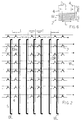
- the memory portion 1 of figure 1 is substantially a block or a sector of memory cells 2, organized into columns, which are called bit line BL, and into rows, called word line WL, according to a traditional structure, so that the cells are selected by standard decoding circuits.
- a plurality of cells 2 and plural decoding devices 3 are present in block 1.
- floating gate MOS devices which form single memory cells 2, and MOS devices 3, which perform the decoding function of the single cells 2, are provided.
- An architecture of the NOR type is proposed; such architecture has a matrix area smaller than the one obtained with an architecture equal to NAND.
- every single non-volatile memory cell 2 comprises a MOS transistor, in which a gate region placed over the channel region is floating, that is such gate region presents a high D.C. impedance towards all the other terminals of the same cell and of the circuit in which the cell is inserted.
- the cell also comprises a second region, called control gate region, which is driven by suitable driving voltages.
- the other transistor electrodes are the usual drain and source terminals.
- the floating gate and control gate regions are formed with respective polysilicon layers, which are insulated one from the other by a dielectric layer.
- control gate regions of cells belonging to the same row are connected with each other through a conduction word line WL.
- Such source and drain regions 4 of the cells are formed by means of some diffusions in active area and are alternatively used as source and drain regions, as it is hereafter described.
- the source and drain regions 4 are in contact with a metal line 5, which forms the bit line BL, for examples every 16 word lines.
- FIG 6 a possible layout of a memory cell 2 is shown. Particularly, on a substrate 2a, for example of the P- type, source and drain regions 4 are formed through, for example, an N+ type implantation into the substrate 2.
- control gate region is also shown; such region is formed by a polysilicon stripe, which is also used to form the word lines.
- the decoding MOS devices 3 comprise a Yn transistor connected with each matrix column. Such Yn transistors are therefore connected with a Ym pass transistor depending on the number of the matrix outputs.
- a second Yna transistor is connected with each matrix column. Such Yna transistors are therefore connected with a second Yma pass transistor.
- the complete memory matrix provides with a plurality of blocks 1. Such blocks 1 are divided by at least an insulation layer 7, as shown in figure 2.
- this insulation layer 7 is a field oxide layer, which is formed between a block and the adjacent one. In such a way cells belonging to adjacent blocks are avoided to be in series. In this embodiment, it is possible to avoid to introduce selection transistors, which would be otherwise necessary to univocally identify a memory cell.
- FIG 2 a preferred embodiment is shown.
- two insulation stripes 7 are arranged, and referring cells 8 are inserted between the two stripes 7.
- the memory blocks 1 are delimited by non-used cell columns, called DUMMY columns.
- this nth cell 2 is obtained by simultaneously connecting the nth bit-line to the circuitry 3 of the column decoding, and therefore to the reading circuitry, as it happens in the prior art and by short-circuiting the ground 1-nth bit line.
- bit line n becomes the drain region of the selected cell 2, while the bit line n- 1 becomes the source region of the same cell.
- the word lines WL are formed in polysilicon and are horizontally placed at a distance equal to the lithographic minimum, with a length equal to the lithographic minimum (min), as shown in figure 6.
- L also indicates the length of the cell 2.
- bit lines BL which are formed through the metal line 5 are vertically placed and are in contact with the active area, which is below each n lines, for example 16 word lines. Also the below active area is vertically placed, without solution of continuity, the whole array long, and forms the cell source or drain regions, depending on the bias voltages.
- bit line BL has been made out of metal and operates as a conductive shunt of the active area layer, therefore improving the resistivety of such layer.
- the vertical stripes of active area have dimensions equal to the lithographic minimum and a distance determined by the desired features of the non-volatile memory cell; such stripes operate as source or drain of the selected cells.
- the matrix decoding method is hereafter described according to the invention.
- the nth cell indicated in figure 1 should be considered as an example.
- Such cell comprises a drain, constituted by the Yn bit line, and of a source, constituted by the Yn- 1 bit line.
- the cell selection is made when for example two decoding levels are used, by enabling a Ym pass transistor of the Yn bit line through the traditional decoding with the Yn signal and by short-circuiting the Yn- 1 bit line through another Yna transistor, which is connected to the second Yma pass transistor, the latter in its turn ground connected.
- Such Yna transistors and the second Yma pass transistor are placed in the bit line area opposite to the column decoding, with the gate region connected to the Yn signal, which is the same signal used in the column decoder.
- the simultaneous selection of the drains and the connection to ground of the cell source are obtained.
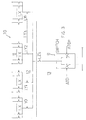
- a particular row decoding circuitry 10 has been advantageously provided. Such circuitry will be hereafter described, making reference to a more general decoding case presenting three levels.
- the switch 9 is driven by the well known ATD (Address Transition Detection) signal, which is always present in a non-volatile memory, and by the complement ATDn signal.
- ATD Address Transition Detection
- the decoding circuitry 10 comprises N-Channel transistors driven on each level by respective Lx, Ly, Lz decoding signals, which have to be suitably boosted as regards to the Vdd supply, during the reading operation, so that the transfer of the total supply to the selected row is allowed.
- the proposed decoding can be formed with only a matallization level and can be particularly used in submicrometric technologies.
- an ATD pulse is generated; such ATD pulse is normally used also to synchronize many operations inside the memory device.
- the ATD signal is also applied to the switch 9, in order to have this switch 9 turning on towards the ground.
- the ground potential is applied on all the word lines, by means of a abilitation of the respective decoding levels 11, 12, 13 through the Lx, Ly, Lz signals.
- the ATDn complement signal forces indeed the switch 9 to the switching, towards the Vdd supply.
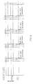
- the switching time duration is schematically shown in figure 4.
- the supply of the Lx, Ly, Lz signals is guaranteed by a charge pump, not shown since it is conventional, which allows a total driving of the pass-transistors to the considered Vdd voltage.
- Each of the decoding signals of the "L" type is obtained by the series of a pair of logic gates.
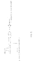
- FIG 5 it is shown a possible circuital structure comprising a gate NOR 14 having two inputs and to which an inverter 15 is cascade connected.
- a first input of the gate NOR 14 receives the ATD signal, while the other input receives an L signal from a pre-decoder, which is not shown since it is conventional.
- the memory matrix according to the invention allows to form a very compact matrix, avoiding the use of the selection transistors and introducing some insulation stripes between the blocks, with a great reduction of the total space.
- the selection of the single memory cells occurs in a simple and effective way, thanks to a pass-transistor decoding circuitry.
- the architecture according to the invention leads to a considerable efficiency gain of the memory cells, since the metal line 5 contacts the source and drain regions every 16 word lines.
- the selection transistors are indeed placed every 64 word lines, with a clear decay of the memory cells performances.
- the source and drain region resistance of the memory cell is advantageously the same.
Landscapes
- Engineering & Computer Science (AREA)
- Microelectronics & Electronic Packaging (AREA)
- Read Only Memory (AREA)
- Non-Volatile Memory (AREA)
- Semiconductor Memories (AREA)
Abstract
Description
- figure 1 shows an electric diagram of a memory matrix block, forming an EPROM or a FLASH-EPROM device according to the invention;
- figure 2 shows an electric diagram of a particular located between two memory matrix blocks according to the invention;
- figure 3 shows a schematic view of a decoding circuitry, which is associated with the matrix of figure 1;
- figure 4 shows a diagram as a function of the time of an ATD signal, which is present in the matrix of figure 1;
- figure 5 shows a particular of the decoding circuitry of figure 3;
- figure 6 shows a possible layout of a matrix memory cell according to the invention.
Claims (12)
- Non-volatile memory matrix architecture with virtual ground monolithically integrated on semiconductor, and of the type comprising a plurality of memory cells (2), each cell having respective source and drain regions (4), which are organized into matrix blocks or sectors placed on rows (WL) and columns (BL) with associated row and column decoding circuits, characterized in that said cell blocks or sectors are separated from each other by at least a insulation stripe, which is parallel to the columns (BL) and in that said source and drain regions are interchangeable.
- Non-volatile memory matrix architecture according to claim 1, charaterized in that said blocks or sectors are separated by two insulation stripes (7) in reciprocal spaced relation.
- Non-volatile memory matrix architecture according to claim 2, characterized in that it comprises referring cells (8), formed between the two insulation stripes (7).
- Non-volatile memory matrix architecture according to any of the previous claims, characterized in that said insulation stripes (7) are made of silicon oxide.
- Non-volatile memory matrix architecture according to claim 1, characterized in that it is a NOR type architecture.
- Non-volatile memory matrix architecture according to claim 1, characterized in that it comprises a pass-transistor row decoding circuitry (10), having a number of levels depending on the number of rows to select.
- Non-volatile memory matrix architecture according to claim 6, characterized in that a selecting switch (9) driven by an ATD signal is associated to said decoding circuitry (10).
- Non-volatile memory matrix architecture according to claim 6, characterized in that said pass-transistors are N-Channel and are driven on each level by respective (Lx, Ly, Lz) signals, which derive from an ATD signal.
- Non-volatile memory matrix architecture according to claim 8, characterized in that said signals are obtained by the ATD signal downstream of a logic gate (14, 15) cascade.
- Non-volatile memory matrix architecture according to claim 1, characterized in that each column (BL) of the matrix is the head of a selection (Ym) pass-transistor, and in that the columns of a block or sector are the heads of a (Ym) pass-transistor of a block selection.
- Non-volatile memory matrix architecture according to claim 1, characterized in that said matrix columns comprise a conductive stripe (5), which is in contact with said source or drain regions (4) every 16 rows.
- Method to select a non-volatile memory cell (2), comprised in a non-volatile memory matrix architecture with virtual ground monolithically integrated on semiconductor, said matrix comprising a plurality of transistor cells (2), with respective source and drain regions, which are organized on rows or word lines (WL), and columns or bit lines (BL) of matrix blocks or sectors, with associated row and column decoding circuits, characterized in that the selection of said cell (2) is obtained by connecting the respective bit lines to corresponding column decoding circuits (3), and simultaneously connecting an adjacent bit line to a reference potential, in such a way that said respective bit line becomes the drain region of the selected cell (2), while the adjacent bit line becomes the source region of the same cell.
Priority Applications (2)
| Application Number | Priority Date | Filing Date | Title |
|---|---|---|---|
| EP00204838A EP1170798B1 (en) | 2000-07-04 | 2000-12-14 | Non-volatile memory matrix architecture |
| US09/898,744 US6466479B2 (en) | 2000-07-04 | 2001-07-03 | Non-volatile memory matrix architecture with vertical insulation strips between adjacent memory blocks |
Applications Claiming Priority (3)
| Application Number | Priority Date | Filing Date | Title |
|---|---|---|---|
| EP00830468 | 2000-07-04 | ||
| EP00830468 | 2000-07-04 | ||
| EP00204838A EP1170798B1 (en) | 2000-07-04 | 2000-12-14 | Non-volatile memory matrix architecture |
Publications (2)
| Publication Number | Publication Date |
|---|---|
| EP1170798A1 true EP1170798A1 (en) | 2002-01-09 |
| EP1170798B1 EP1170798B1 (en) | 2006-09-06 |
Family
ID=26072930
Family Applications (1)
| Application Number | Title | Priority Date | Filing Date |
|---|---|---|---|
| EP00204838A Expired - Lifetime EP1170798B1 (en) | 2000-07-04 | 2000-12-14 | Non-volatile memory matrix architecture |
Country Status (2)
| Country | Link |
|---|---|
| US (1) | US6466479B2 (en) |
| EP (1) | EP1170798B1 (en) |
Families Citing this family (5)
| Publication number | Priority date | Publication date | Assignee | Title |
|---|---|---|---|---|
| JP3906177B2 (en) * | 2002-05-10 | 2007-04-18 | 株式会社東芝 | Nonvolatile semiconductor memory device |
| US7623118B2 (en) * | 2005-03-14 | 2009-11-24 | Palm, Inc. | Actuation mechanism for use with keyboards on mobile computing devices |
| EP1845532B1 (en) * | 2006-04-12 | 2009-04-01 | STMicroelectronics S.r.l. | A column decoding system for semiconductor memory devices implemented with low voltage transistors |
| JP2010056443A (en) * | 2008-08-29 | 2010-03-11 | Toshiba Corp | Nonvolatile semiconductor memory and method of manufacturing the same |
| US20150071020A1 (en) * | 2013-09-06 | 2015-03-12 | Sony Corporation | Memory device comprising tiles with shared read and write circuits |
Citations (5)
| Publication number | Priority date | Publication date | Assignee | Title |
|---|---|---|---|---|
| US5200350A (en) * | 1988-11-10 | 1993-04-06 | Texas Instruments Incorporated | Floating-gate memory array with silicided buried bitlines |
| EP0552531A1 (en) * | 1992-01-22 | 1993-07-28 | Macronix International Co., Ltd. | Non-volatile memory cell and array architecture |
| WO1996008840A1 (en) * | 1994-09-13 | 1996-03-21 | Macronix International Co., Ltd. | A flash eprom transistor array and method for manufacturing the same |
| EP0854514A1 (en) * | 1997-01-15 | 1998-07-22 | Macronix International Co., Ltd. | An asymmetric cell for a semiconductor memory array and a manufacturing method therefor |
| US6040234A (en) * | 1996-07-30 | 2000-03-21 | Nec Corporation | Method of manufacturing semiconductor device without bird beak effect |
Family Cites Families (4)
| Publication number | Priority date | Publication date | Assignee | Title |
|---|---|---|---|---|
| US5428621A (en) * | 1992-09-21 | 1995-06-27 | Sundisk Corporation | Latent defect handling in EEPROM devices |
| US5748535A (en) * | 1994-10-26 | 1998-05-05 | Macronix International Co., Ltd. | Advanced program verify for page mode flash memory |
| US5646886A (en) * | 1995-05-24 | 1997-07-08 | National Semiconductor Corporation | Flash memory having segmented array for improved operation |
| US5787039A (en) * | 1997-03-06 | 1998-07-28 | Macronix International Co., Ltd. | Low current floating gate programming with bit-by-bit verification |
-
2000
- 2000-12-14 EP EP00204838A patent/EP1170798B1/en not_active Expired - Lifetime
-
2001
- 2001-07-03 US US09/898,744 patent/US6466479B2/en not_active Expired - Lifetime
Patent Citations (5)
| Publication number | Priority date | Publication date | Assignee | Title |
|---|---|---|---|---|
| US5200350A (en) * | 1988-11-10 | 1993-04-06 | Texas Instruments Incorporated | Floating-gate memory array with silicided buried bitlines |
| EP0552531A1 (en) * | 1992-01-22 | 1993-07-28 | Macronix International Co., Ltd. | Non-volatile memory cell and array architecture |
| WO1996008840A1 (en) * | 1994-09-13 | 1996-03-21 | Macronix International Co., Ltd. | A flash eprom transistor array and method for manufacturing the same |
| US6040234A (en) * | 1996-07-30 | 2000-03-21 | Nec Corporation | Method of manufacturing semiconductor device without bird beak effect |
| EP0854514A1 (en) * | 1997-01-15 | 1998-07-22 | Macronix International Co., Ltd. | An asymmetric cell for a semiconductor memory array and a manufacturing method therefor |
Also Published As
| Publication number | Publication date |
|---|---|
| US6466479B2 (en) | 2002-10-15 |
| US20020021582A1 (en) | 2002-02-21 |
| EP1170798B1 (en) | 2006-09-06 |
Similar Documents
| Publication | Publication Date | Title |
|---|---|---|
| US6285574B1 (en) | Symmetric segmented memory array architecture | |
| US6570810B2 (en) | Contactless flash memory with buried diffusion bit/virtual ground lines | |
| US5432730A (en) | Electrically programmable read only memory array | |
| US6218695B1 (en) | Area efficient column select circuitry for 2-bit non-volatile memory cells | |
| US5590068A (en) | Ultra-high density alternate metal virtual ground ROM | |
| KR100304750B1 (en) | Semiconductor memory device | |
| US5596523A (en) | Electrically erasable programmable read-only memory with an array of one-transistor memory cells | |
| US5233559A (en) | Row redundancy for flash memories | |
| US6760267B2 (en) | Segmented non-volatile memory array with multiple sources having improved source line decode circuitry | |
| WO1996008824A1 (en) | Eprom array segmented for high performance and method for controlling same | |
| EP0880144A2 (en) | Read only memory | |
| US5105385A (en) | Cell array pattern layout for eeprom device | |
| US6031771A (en) | Memory redundancy circuit using single polysilicon floating gate transistors as redundancy elements | |
| US5313420A (en) | Programmable semiconductor memory | |
| US5355332A (en) | Electrically erasable programmable read-only memory with an array of one-transistor memory cells | |
| EP1170798B1 (en) | Non-volatile memory matrix architecture | |
| EP0035646B1 (en) | Integrated semiconductor memory matrix using one-fet cells | |
| US6215688B1 (en) | Electronic memory circuit and related manufacturing method | |
| EP0946988B1 (en) | Memory redundancy circuit using single polysilicon floating gate transistors as redundancy elements | |
| JPH0762960B2 (en) | Semiconductor circuit | |
| US5663903A (en) | Flat-cell read-only memory | |
| EP0508552B1 (en) | Programmable semiconductor memory | |
| US5245566A (en) | Programmable semiconductor | |
| KR100666289B1 (en) | Integrated Circuit Memory with Partitioned Well Structure | |
| JPH0673240B2 (en) | Read-only semiconductor memory |
Legal Events
| Date | Code | Title | Description |
|---|---|---|---|
| PUAI | Public reference made under article 153(3) epc to a published international application that has entered the european phase |
Free format text: ORIGINAL CODE: 0009012 |
|
| AK | Designated contracting states |
Kind code of ref document: A1 Designated state(s): DE FR GB IT Kind code of ref document: A1 Designated state(s): AT BE CH CY DE DK ES FI FR GB GR IE IT LI LU MC NL PT SE TR |
|
| AX | Request for extension of the european patent |
Free format text: AL;LT;LV;MK;RO;SI |
|
| 17P | Request for examination filed |
Effective date: 20020315 |
|
| AKX | Designation fees paid |
Free format text: DE FR GB IT |
|
| 17Q | First examination report despatched |
Effective date: 20021011 |
|
| GRAP | Despatch of communication of intention to grant a patent |
Free format text: ORIGINAL CODE: EPIDOSNIGR1 |
|
| GRAS | Grant fee paid |
Free format text: ORIGINAL CODE: EPIDOSNIGR3 |
|
| GRAA | (expected) grant |
Free format text: ORIGINAL CODE: 0009210 |
|
| AK | Designated contracting states |
Kind code of ref document: B1 Designated state(s): DE FR GB IT |
|
| REG | Reference to a national code |
Ref country code: GB Ref legal event code: FG4D |
|
| REF | Corresponds to: |
Ref document number: 60030546 Country of ref document: DE Date of ref document: 20061019 Kind code of ref document: P |
|
| PG25 | Lapsed in a contracting state [announced via postgrant information from national office to epo] |
Ref country code: DE Free format text: LAPSE BECAUSE OF FAILURE TO SUBMIT A TRANSLATION OF THE DESCRIPTION OR TO PAY THE FEE WITHIN THE PRESCRIBED TIME-LIMIT Effective date: 20061207 |
|
| ET | Fr: translation filed | ||
| PLBE | No opposition filed within time limit |
Free format text: ORIGINAL CODE: 0009261 |
|
| STAA | Information on the status of an ep patent application or granted ep patent |
Free format text: STATUS: NO OPPOSITION FILED WITHIN TIME LIMIT |
|
| 26N | No opposition filed |
Effective date: 20070607 |
|
| PGFP | Annual fee paid to national office [announced via postgrant information from national office to epo] |
Ref country code: IT Payment date: 20071211 Year of fee payment: 8 |
|
| PGFP | Annual fee paid to national office [announced via postgrant information from national office to epo] |
Ref country code: GB Payment date: 20081125 Year of fee payment: 9 |
|
| PGFP | Annual fee paid to national office [announced via postgrant information from national office to epo] |
Ref country code: FR Payment date: 20081224 Year of fee payment: 9 |
|
| GBPC | Gb: european patent ceased through non-payment of renewal fee |
Effective date: 20091214 |
|
| REG | Reference to a national code |
Ref country code: FR Ref legal event code: ST Effective date: 20100831 |
|
| PG25 | Lapsed in a contracting state [announced via postgrant information from national office to epo] |
Ref country code: FR Free format text: LAPSE BECAUSE OF NON-PAYMENT OF DUE FEES Effective date: 20091231 |
|
| PG25 | Lapsed in a contracting state [announced via postgrant information from national office to epo] |
Ref country code: GB Free format text: LAPSE BECAUSE OF NON-PAYMENT OF DUE FEES Effective date: 20091214 |
|
| PG25 | Lapsed in a contracting state [announced via postgrant information from national office to epo] |
Ref country code: IT Free format text: LAPSE BECAUSE OF NON-PAYMENT OF DUE FEES Effective date: 20081214 |