EP1170273A1 - Alkynic compounds, their use as monomers in vacuum deposition polymerisation, thin films formed from these polymers and their use in electroluminescent devices - Google Patents
Alkynic compounds, their use as monomers in vacuum deposition polymerisation, thin films formed from these polymers and their use in electroluminescent devices Download PDFInfo
- Publication number
- EP1170273A1 EP1170273A1 EP01100286A EP01100286A EP1170273A1 EP 1170273 A1 EP1170273 A1 EP 1170273A1 EP 01100286 A EP01100286 A EP 01100286A EP 01100286 A EP01100286 A EP 01100286A EP 1170273 A1 EP1170273 A1 EP 1170273A1
- Authority
- EP
- European Patent Office
- Prior art keywords
- thin film
- irradiation
- layer
- vacuum deposition
- polymerization
- Prior art date
- Legal status (The legal status is an assumption and is not a legal conclusion. Google has not performed a legal analysis and makes no representation as to the accuracy of the status listed.)
- Granted
Links
- 239000010409 thin film Substances 0.000 title claims abstract description 48
- 238000001771 vacuum deposition Methods 0.000 title claims abstract description 32
- 229920000642 polymer Polymers 0.000 title claims abstract description 13
- 150000001875 compounds Chemical class 0.000 title description 10
- 239000000178 monomer Substances 0.000 title description 2
- 238000006116 polymerization reaction Methods 0.000 claims abstract description 52
- 238000009281 ultraviolet germicidal irradiation Methods 0.000 claims abstract description 25
- 125000002534 ethynyl group Chemical group [H]C#C* 0.000 claims abstract description 22
- 150000002894 organic compounds Chemical class 0.000 claims abstract description 21
- 238000005401 electroluminescence Methods 0.000 claims abstract description 16
- 239000000758 substrate Substances 0.000 claims abstract description 15
- 238000010438 heat treatment Methods 0.000 claims abstract description 12
- 238000000151 deposition Methods 0.000 claims description 33
- 238000001029 thermal curing Methods 0.000 claims description 23
- 230000005525 hole transport Effects 0.000 claims description 11
- 230000000379 polymerizing effect Effects 0.000 claims description 9
- 229910052751 metal Inorganic materials 0.000 claims description 5
- 239000002184 metal Substances 0.000 claims description 5
- 125000004435 hydrogen atom Chemical group [H]* 0.000 claims description 4
- 229930195733 hydrocarbon Natural products 0.000 claims description 2
- UHOVQNZJYSORNB-UHFFFAOYSA-N Benzene Chemical compound C1=CC=CC=C1 UHOVQNZJYSORNB-UHFFFAOYSA-N 0.000 description 48
- 239000010410 layer Substances 0.000 description 38
- 230000008021 deposition Effects 0.000 description 28
- QGICIDGCKPUALM-UHFFFAOYSA-N 4-ethynyl-n,n-bis(4-ethynylphenyl)aniline Chemical compound C1=CC(C#C)=CC=C1N(C=1C=CC(=CC=1)C#C)C1=CC=C(C#C)C=C1 QGICIDGCKPUALM-UHFFFAOYSA-N 0.000 description 23
- RTZKZFJDLAIYFH-UHFFFAOYSA-N Diethyl ether Chemical compound CCOCC RTZKZFJDLAIYFH-UHFFFAOYSA-N 0.000 description 20
- BPOXHIPLBUUYGO-UHFFFAOYSA-N 2,7-diethynyl-9h-fluorene Chemical compound C#CC1=CC=C2C3=CC=C(C#C)C=C3CC2=C1 BPOXHIPLBUUYGO-UHFFFAOYSA-N 0.000 description 18
- QTZDQTKYFDGVDN-UHFFFAOYSA-N 2-ethynyl-9h-fluorene Chemical compound C1=CC=C2C3=CC=C(C#C)C=C3CC2=C1 QTZDQTKYFDGVDN-UHFFFAOYSA-N 0.000 description 17
- 239000011541 reaction mixture Substances 0.000 description 17
- OKKJLVBELUTLKV-UHFFFAOYSA-N Methanol Chemical compound OC OKKJLVBELUTLKV-UHFFFAOYSA-N 0.000 description 15
- 238000000034 method Methods 0.000 description 15
- HEDRZPFGACZZDS-UHFFFAOYSA-N Chloroform Chemical compound ClC(Cl)Cl HEDRZPFGACZZDS-UHFFFAOYSA-N 0.000 description 12
- XEKOWRVHYACXOJ-UHFFFAOYSA-N Ethyl acetate Chemical compound CCOC(C)=O XEKOWRVHYACXOJ-UHFFFAOYSA-N 0.000 description 12
- VLKZOEOYAKHREP-UHFFFAOYSA-N n-Hexane Chemical compound CCCCCC VLKZOEOYAKHREP-UHFFFAOYSA-N 0.000 description 12
- 239000002904 solvent Substances 0.000 description 12
- 239000012153 distilled water Substances 0.000 description 11
- XLYOFNOQVPJJNP-UHFFFAOYSA-N water Chemical compound O XLYOFNOQVPJJNP-UHFFFAOYSA-N 0.000 description 11
- UAOMVDZJSHZZME-UHFFFAOYSA-N diisopropylamine Chemical compound CC(C)NC(C)C UAOMVDZJSHZZME-UHFFFAOYSA-N 0.000 description 9
- 238000002360 preparation method Methods 0.000 description 9
- 239000002243 precursor Substances 0.000 description 8
- 238000002329 infrared spectrum Methods 0.000 description 7
- -1 poly(p-xylylene) Polymers 0.000 description 7
- 238000012643 polycondensation polymerization Methods 0.000 description 7
- 150000003254 radicals Chemical class 0.000 description 7
- CWMFRHBXRUITQE-UHFFFAOYSA-N trimethylsilylacetylene Chemical group C[Si](C)(C)C#C CWMFRHBXRUITQE-UHFFFAOYSA-N 0.000 description 7
- QTBSBXVTEAMEQO-UHFFFAOYSA-N Acetic acid Chemical compound CC(O)=O QTBSBXVTEAMEQO-UHFFFAOYSA-N 0.000 description 6
- WYURNTSHIVDZCO-UHFFFAOYSA-N Tetrahydrofuran Chemical compound C1CCOC1 WYURNTSHIVDZCO-UHFFFAOYSA-N 0.000 description 6
- 238000000862 absorption spectrum Methods 0.000 description 6
- HFACYLZERDEVSX-UHFFFAOYSA-N benzidine Chemical compound C1=CC(N)=CC=C1C1=CC=C(N)C=C1 HFACYLZERDEVSX-UHFFFAOYSA-N 0.000 description 6
- 239000012043 crude product Substances 0.000 description 6
- 238000000921 elemental analysis Methods 0.000 description 6
- 239000010408 film Substances 0.000 description 6
- 125000000040 m-tolyl group Chemical group [H]C1=C([H])C(*)=C([H])C(=C1[H])C([H])([H])[H] 0.000 description 6
- 239000002244 precipitate Substances 0.000 description 6
- ORILYTVJVMAKLC-UHFFFAOYSA-N adamantane Chemical compound C1C(C2)CC3CC1CC2C3 ORILYTVJVMAKLC-UHFFFAOYSA-N 0.000 description 5
- 238000001938 differential scanning calorimetry curve Methods 0.000 description 5
- WVOIHKKFEONCBV-UHFFFAOYSA-N n-[4-[4-(4-bromo-n-(3-methylphenyl)anilino)phenyl]phenyl]-n-(4-bromophenyl)-3-methylaniline Chemical compound CC1=CC=CC(N(C=2C=CC(Br)=CC=2)C=2C=CC(=CC=2)C=2C=CC(=CC=2)N(C=2C=CC(Br)=CC=2)C=2C=C(C)C=CC=2)=C1 WVOIHKKFEONCBV-UHFFFAOYSA-N 0.000 description 5
- KWYUFKZDYYNOTN-UHFFFAOYSA-M Potassium hydroxide Chemical compound [OH-].[K+] KWYUFKZDYYNOTN-UHFFFAOYSA-M 0.000 description 4
- VYPSYNLAJGMNEJ-UHFFFAOYSA-N Silicium dioxide Chemical compound O=[Si]=O VYPSYNLAJGMNEJ-UHFFFAOYSA-N 0.000 description 4
- 229910001573 adamantine Inorganic materials 0.000 description 4
- 239000006227 byproduct Substances 0.000 description 4
- 238000004440 column chromatography Methods 0.000 description 4
- GBRBMTNGQBKBQE-UHFFFAOYSA-L copper;diiodide Chemical compound I[Cu]I GBRBMTNGQBKBQE-UHFFFAOYSA-L 0.000 description 4
- YNHIGQDRGKUECZ-UHFFFAOYSA-N dichloropalladium;triphenylphosphanium Chemical compound Cl[Pd]Cl.C1=CC=CC=C1[PH+](C=1C=CC=CC=1)C1=CC=CC=C1.C1=CC=CC=C1[PH+](C=1C=CC=CC=1)C1=CC=CC=C1 YNHIGQDRGKUECZ-UHFFFAOYSA-N 0.000 description 4
- DMBHHRLKUKUOEG-UHFFFAOYSA-N diphenylamine Chemical compound C=1C=CC=CC=1NC1=CC=CC=C1 DMBHHRLKUKUOEG-UHFFFAOYSA-N 0.000 description 4
- 229940093499 ethyl acetate Drugs 0.000 description 4
- 235000019439 ethyl acetate Nutrition 0.000 description 4
- 239000011521 glass Substances 0.000 description 4
- 238000000655 nuclear magnetic resonance spectrum Methods 0.000 description 4
- 238000003847 radiation curing Methods 0.000 description 4
- 239000004065 semiconductor Substances 0.000 description 4
- 239000000741 silica gel Substances 0.000 description 4
- 229910002027 silica gel Inorganic materials 0.000 description 4
- TVIVIEFSHFOWTE-UHFFFAOYSA-K tri(quinolin-8-yloxy)alumane Chemical compound [Al+3].C1=CN=C2C([O-])=CC=CC2=C1.C1=CN=C2C([O-])=CC=CC2=C1.C1=CN=C2C([O-])=CC=CC2=C1 TVIVIEFSHFOWTE-UHFFFAOYSA-K 0.000 description 4
- IEZMHEVAKUKLKB-UHFFFAOYSA-N 2-(4-ethynylphenyl)-1,3,4-oxadiazole Chemical compound C(#C)C1=CC=C(C=C1)C1=NN=CO1 IEZMHEVAKUKLKB-UHFFFAOYSA-N 0.000 description 3
- IIPDKVKBZNLDMD-UHFFFAOYSA-N 9,10-diethynylanthracene Chemical compound C1=CC=C2C(C#C)=C(C=CC=C3)C3=C(C#C)C2=C1 IIPDKVKBZNLDMD-UHFFFAOYSA-N 0.000 description 3
- KFZMGEQAYNKOFK-UHFFFAOYSA-N Isopropanol Chemical compound CC(C)O KFZMGEQAYNKOFK-UHFFFAOYSA-N 0.000 description 3
- XUIMIQQOPSSXEZ-UHFFFAOYSA-N Silicon Chemical compound [Si] XUIMIQQOPSSXEZ-UHFFFAOYSA-N 0.000 description 3
- ZMANZCXQSJIPKH-UHFFFAOYSA-N Triethylamine Chemical compound CCN(CC)CC ZMANZCXQSJIPKH-UHFFFAOYSA-N 0.000 description 3
- 150000001491 aromatic compounds Chemical class 0.000 description 3
- 229940043279 diisopropylamine Drugs 0.000 description 3
- RMBPEFMHABBEKP-UHFFFAOYSA-N fluorene Chemical compound C1=CC=C2C3=C[CH]C=CC3=CC2=C1 RMBPEFMHABBEKP-UHFFFAOYSA-N 0.000 description 3
- 239000011229 interlayer Substances 0.000 description 3
- 238000004519 manufacturing process Methods 0.000 description 3
- 239000000203 mixture Substances 0.000 description 3
- NIHNNTQXNPWCJQ-UHFFFAOYSA-N o-biphenylenemethane Natural products C1=CC=C2CC3=CC=CC=C3C2=C1 NIHNNTQXNPWCJQ-UHFFFAOYSA-N 0.000 description 3
- 230000003287 optical effect Effects 0.000 description 3
- NLKNQRATVPKPDG-UHFFFAOYSA-M potassium iodide Chemical compound [K+].[I-] NLKNQRATVPKPDG-UHFFFAOYSA-M 0.000 description 3
- 229910052710 silicon Inorganic materials 0.000 description 3
- 239000010703 silicon Substances 0.000 description 3
- 239000000243 solution Substances 0.000 description 3
- YLQBMQCUIZJEEH-UHFFFAOYSA-N tetrahydrofuran Natural products C=1C=COC=1 YLQBMQCUIZJEEH-UHFFFAOYSA-N 0.000 description 3
- 238000002411 thermogravimetry Methods 0.000 description 3
- AVXFJPFSWLMKSG-UHFFFAOYSA-N 2,7-dibromo-9h-fluorene Chemical compound BrC1=CC=C2C3=CC=C(Br)C=C3CC2=C1 AVXFJPFSWLMKSG-UHFFFAOYSA-N 0.000 description 2
- NVWPJCSJDSNVON-UHFFFAOYSA-N 2-(9h-fluoren-1-yl)ethynyl-trimethylsilane Chemical compound C1C2=CC=CC=C2C2=C1C(C#C[Si](C)(C)C)=CC=C2 NVWPJCSJDSNVON-UHFFFAOYSA-N 0.000 description 2
- VNYQUOAQPXGXQO-UHFFFAOYSA-N 2-iodo-9h-fluorene Chemical compound C1=CC=C2C3=CC=C(I)C=C3CC2=C1 VNYQUOAQPXGXQO-UHFFFAOYSA-N 0.000 description 2
- WWJQYSYANNGAAC-UHFFFAOYSA-N 4-(2-trimethylsilylethynyl)-n,n-bis[4-(2-trimethylsilylethynyl)phenyl]aniline Chemical compound C1=CC(C#C[Si](C)(C)C)=CC=C1N(C=1C=CC(=CC=1)C#C[Si](C)(C)C)C1=CC=C(C#C[Si](C)(C)C)C=C1 WWJQYSYANNGAAC-UHFFFAOYSA-N 0.000 description 2
- ZRXVCYGHAUGABY-UHFFFAOYSA-N 4-bromo-n,n-bis(4-bromophenyl)aniline Chemical compound C1=CC(Br)=CC=C1N(C=1C=CC(Br)=CC=1)C1=CC=C(Br)C=C1 ZRXVCYGHAUGABY-UHFFFAOYSA-N 0.000 description 2
- SQTLUXJWUCHKMT-UHFFFAOYSA-N 4-bromo-n,n-diphenylaniline Chemical compound C1=CC(Br)=CC=C1N(C=1C=CC=CC=1)C1=CC=CC=C1 SQTLUXJWUCHKMT-UHFFFAOYSA-N 0.000 description 2
- CSCPPACGZOOCGX-UHFFFAOYSA-N Acetone Chemical compound CC(C)=O CSCPPACGZOOCGX-UHFFFAOYSA-N 0.000 description 2
- WKBOTKDWSSQWDR-UHFFFAOYSA-N Bromine atom Chemical compound [Br] WKBOTKDWSSQWDR-UHFFFAOYSA-N 0.000 description 2
- LFQSCWFLJHTTHZ-UHFFFAOYSA-N Ethanol Chemical compound CCO LFQSCWFLJHTTHZ-UHFFFAOYSA-N 0.000 description 2
- KDLHZDBZIXYQEI-UHFFFAOYSA-N Palladium Chemical compound [Pd] KDLHZDBZIXYQEI-UHFFFAOYSA-N 0.000 description 2
- QAOWNCQODCNURD-UHFFFAOYSA-N Sulfuric acid Chemical compound OS(O)(=O)=O QAOWNCQODCNURD-UHFFFAOYSA-N 0.000 description 2
- 238000010521 absorption reaction Methods 0.000 description 2
- 229910052782 aluminium Inorganic materials 0.000 description 2
- XAGFODPZIPBFFR-UHFFFAOYSA-N aluminium Chemical compound [Al] XAGFODPZIPBFFR-UHFFFAOYSA-N 0.000 description 2
- 150000001499 aryl bromides Chemical class 0.000 description 2
- 150000001503 aryl iodides Chemical class 0.000 description 2
- GDTBXPJZTBHREO-UHFFFAOYSA-N bromine Substances BrBr GDTBXPJZTBHREO-UHFFFAOYSA-N 0.000 description 2
- 229910052794 bromium Inorganic materials 0.000 description 2
- 239000003054 catalyst Substances 0.000 description 2
- 238000006243 chemical reaction Methods 0.000 description 2
- 238000011109 contamination Methods 0.000 description 2
- 239000003989 dielectric material Substances 0.000 description 2
- NROKBHXJSPEDAR-UHFFFAOYSA-M potassium fluoride Chemical compound [F-].[K+] NROKBHXJSPEDAR-UHFFFAOYSA-M 0.000 description 2
- 239000011698 potassium fluoride Substances 0.000 description 2
- 230000005855 radiation Effects 0.000 description 2
- 239000007787 solid Substances 0.000 description 2
- 238000001757 thermogravimetry curve Methods 0.000 description 2
- JENARGOADBRORO-UHFFFAOYSA-N trimethyl-[2-[7-(2-trimethylsilylethynyl)-9h-fluoren-2-yl]ethynyl]silane Chemical compound C[Si](C)(C)C#CC1=CC=C2C3=CC=C(C#C[Si](C)(C)C)C=C3CC2=C1 JENARGOADBRORO-UHFFFAOYSA-N 0.000 description 2
- 230000008016 vaporization Effects 0.000 description 2
- XSICYCAIFVIORL-UHFFFAOYSA-N 1,4-diphenyladamantane Chemical compound C1C(C2)CC3CC2(C=2C=CC=CC=2)CC1C3C1=CC=CC=C1 XSICYCAIFVIORL-UHFFFAOYSA-N 0.000 description 1
- UGBVZNXXRZISHN-UHFFFAOYSA-N 2-(4-bromophenyl)-1,3,4-oxadiazole Chemical compound C1=CC(Br)=CC=C1C1=NN=CO1 UGBVZNXXRZISHN-UHFFFAOYSA-N 0.000 description 1
- ZCYVEMRRCGMTRW-UHFFFAOYSA-N 7553-56-2 Chemical compound [I] ZCYVEMRRCGMTRW-UHFFFAOYSA-N 0.000 description 1
- BRUOAURMAFDGLP-UHFFFAOYSA-N 9,10-dibromoanthracene Chemical compound C1=CC=C2C(Br)=C(C=CC=C3)C3=C(Br)C2=C1 BRUOAURMAFDGLP-UHFFFAOYSA-N 0.000 description 1
- PJDSQBCKDSTBJB-UHFFFAOYSA-N Cc(cc1)ccc1-c1nnc(-c(cc2)ccc2-c2nnc(-c(cc3)ccc3C#C)[o]2)[o]1 Chemical compound Cc(cc1)ccc1-c1nnc(-c(cc2)ccc2-c2nnc(-c(cc3)ccc3C#C)[o]2)[o]1 PJDSQBCKDSTBJB-UHFFFAOYSA-N 0.000 description 1
- PCLIMKBDDGJMGD-UHFFFAOYSA-N N-bromosuccinimide Chemical compound BrN1C(=O)CCC1=O PCLIMKBDDGJMGD-UHFFFAOYSA-N 0.000 description 1
- GRYLNZFGIOXLOG-UHFFFAOYSA-N Nitric acid Chemical compound O[N+]([O-])=O GRYLNZFGIOXLOG-UHFFFAOYSA-N 0.000 description 1
- ZYGHJZDHTFUPRJ-UHFFFAOYSA-N O=C1Oc2ccccc2C=C1 Chemical compound O=C1Oc2ccccc2C=C1 ZYGHJZDHTFUPRJ-UHFFFAOYSA-N 0.000 description 1
- 239000004952 Polyamide Substances 0.000 description 1
- 239000004642 Polyimide Substances 0.000 description 1
- 229920002396 Polyurea Polymers 0.000 description 1
- PMZURENOXWZQFD-UHFFFAOYSA-L Sodium Sulfate Chemical compound [Na+].[Na+].[O-]S([O-])(=O)=O PMZURENOXWZQFD-UHFFFAOYSA-L 0.000 description 1
- 239000004809 Teflon Substances 0.000 description 1
- 229920006362 Teflon® Polymers 0.000 description 1
- 239000007983 Tris buffer Substances 0.000 description 1
- 230000015572 biosynthetic process Effects 0.000 description 1
- 125000001246 bromo group Chemical group Br* 0.000 description 1
- 239000011248 coating agent Substances 0.000 description 1
- 238000000576 coating method Methods 0.000 description 1
- SWXVUIWOUIDPGS-UHFFFAOYSA-N diacetone alcohol Natural products CC(=O)CC(C)(C)O SWXVUIWOUIDPGS-UHFFFAOYSA-N 0.000 description 1
- 238000003618 dip coating Methods 0.000 description 1
- 238000001035 drying Methods 0.000 description 1
- 238000001194 electroluminescence spectrum Methods 0.000 description 1
- 238000005516 engineering process Methods 0.000 description 1
- 230000002349 favourable effect Effects 0.000 description 1
- 239000012467 final product Substances 0.000 description 1
- 239000012535 impurity Substances 0.000 description 1
- 229910052740 iodine Inorganic materials 0.000 description 1
- 239000011630 iodine Substances 0.000 description 1
- 125000002346 iodo group Chemical group I* 0.000 description 1
- 239000004973 liquid crystal related substance Substances 0.000 description 1
- 229920002521 macromolecule Polymers 0.000 description 1
- 239000000463 material Substances 0.000 description 1
- 239000008204 material by function Substances 0.000 description 1
- 229910017604 nitric acid Inorganic materials 0.000 description 1
- 229920000620 organic polymer Polymers 0.000 description 1
- 229910052763 palladium Inorganic materials 0.000 description 1
- 239000003415 peat Substances 0.000 description 1
- 239000003208 petroleum Substances 0.000 description 1
- 229920002120 photoresistant polymer Polymers 0.000 description 1
- 229920000052 poly(p-xylylene) Polymers 0.000 description 1
- 229920000553 poly(phenylenevinylene) Polymers 0.000 description 1
- 229920002647 polyamide Polymers 0.000 description 1
- 229920001721 polyimide Polymers 0.000 description 1
- 235000003270 potassium fluoride Nutrition 0.000 description 1
- RUOJZAUFBMNUDX-UHFFFAOYSA-N propylene carbonate Chemical compound CC1COC(=O)O1 RUOJZAUFBMNUDX-UHFFFAOYSA-N 0.000 description 1
- AKHNMLFCWUSKQB-UHFFFAOYSA-L sodium thiosulfate Chemical compound [Na+].[Na+].[O-]S([O-])(=O)=S AKHNMLFCWUSKQB-UHFFFAOYSA-L 0.000 description 1
- 235000019345 sodium thiosulphate Nutrition 0.000 description 1
- 238000001228 spectrum Methods 0.000 description 1
- 238000004528 spin coating Methods 0.000 description 1
- 238000003756 stirring Methods 0.000 description 1
- 238000000859 sublimation Methods 0.000 description 1
- 230000008022 sublimation Effects 0.000 description 1
- 125000000026 trimethylsilyl group Chemical group [H]C([H])([H])[Si]([*])(C([H])([H])[H])C([H])([H])[H] 0.000 description 1
- ODHXBMXNKOYIBV-UHFFFAOYSA-N triphenylamine Chemical compound C1=CC=CC=C1N(C=1C=CC=CC=1)C1=CC=CC=C1 ODHXBMXNKOYIBV-UHFFFAOYSA-N 0.000 description 1
Images



Classifications
-
- C—CHEMISTRY; METALLURGY
- C07—ORGANIC CHEMISTRY
- C07C—ACYCLIC OR CARBOCYCLIC COMPOUNDS
- C07C15/00—Cyclic hydrocarbons containing only six-membered aromatic rings as cyclic parts
- C07C15/40—Cyclic hydrocarbons containing only six-membered aromatic rings as cyclic parts substituted by unsaturated carbon radicals
- C07C15/42—Cyclic hydrocarbons containing only six-membered aromatic rings as cyclic parts substituted by unsaturated carbon radicals monocyclic
- C07C15/48—Cyclic hydrocarbons containing only six-membered aromatic rings as cyclic parts substituted by unsaturated carbon radicals monocyclic the hydrocarbon substituent containing a carbon-to-carbon triple bond
-
- C—CHEMISTRY; METALLURGY
- C07—ORGANIC CHEMISTRY
- C07C—ACYCLIC OR CARBOCYCLIC COMPOUNDS
- C07C13/00—Cyclic hydrocarbons containing rings other than, or in addition to, six-membered aromatic rings
- C07C13/28—Polycyclic hydrocarbons or acyclic hydrocarbon derivatives thereof
- C07C13/32—Polycyclic hydrocarbons or acyclic hydrocarbon derivatives thereof with condensed rings
- C07C13/54—Polycyclic hydrocarbons or acyclic hydrocarbon derivatives thereof with condensed rings with three condensed rings
- C07C13/547—Polycyclic hydrocarbons or acyclic hydrocarbon derivatives thereof with condensed rings with three condensed rings at least one ring not being six-membered, the other rings being at the most six-membered
- C07C13/567—Polycyclic hydrocarbons or acyclic hydrocarbon derivatives thereof with condensed rings with three condensed rings at least one ring not being six-membered, the other rings being at the most six-membered with a fluorene or hydrogenated fluorene ring system
-
- C—CHEMISTRY; METALLURGY
- C07—ORGANIC CHEMISTRY
- C07C—ACYCLIC OR CARBOCYCLIC COMPOUNDS
- C07C15/00—Cyclic hydrocarbons containing only six-membered aromatic rings as cyclic parts
- C07C15/20—Polycyclic condensed hydrocarbons
- C07C15/27—Polycyclic condensed hydrocarbons containing three rings
- C07C15/28—Anthracenes
-
- C—CHEMISTRY; METALLURGY
- C07—ORGANIC CHEMISTRY
- C07C—ACYCLIC OR CARBOCYCLIC COMPOUNDS
- C07C211/00—Compounds containing amino groups bound to a carbon skeleton
- C07C211/43—Compounds containing amino groups bound to a carbon skeleton having amino groups bound to carbon atoms of six-membered aromatic rings of the carbon skeleton
- C07C211/54—Compounds containing amino groups bound to a carbon skeleton having amino groups bound to carbon atoms of six-membered aromatic rings of the carbon skeleton having amino groups bound to two or three six-membered aromatic rings
-
- C—CHEMISTRY; METALLURGY
- C07—ORGANIC CHEMISTRY
- C07D—HETEROCYCLIC COMPOUNDS
- C07D271/00—Heterocyclic compounds containing five-membered rings having two nitrogen atoms and one oxygen atom as the only ring hetero atoms
- C07D271/02—Heterocyclic compounds containing five-membered rings having two nitrogen atoms and one oxygen atom as the only ring hetero atoms not condensed with other rings
- C07D271/10—1,3,4-Oxadiazoles; Hydrogenated 1,3,4-oxadiazoles
- C07D271/107—1,3,4-Oxadiazoles; Hydrogenated 1,3,4-oxadiazoles with two aryl or substituted aryl radicals attached in positions 2 and 5
-
- C—CHEMISTRY; METALLURGY
- C07—ORGANIC CHEMISTRY
- C07D—HETEROCYCLIC COMPOUNDS
- C07D333/00—Heterocyclic compounds containing five-membered rings having one sulfur atom as the only ring hetero atom
- C07D333/02—Heterocyclic compounds containing five-membered rings having one sulfur atom as the only ring hetero atom not condensed with other rings
- C07D333/04—Heterocyclic compounds containing five-membered rings having one sulfur atom as the only ring hetero atom not condensed with other rings not substituted on the ring sulphur atom
- C07D333/06—Heterocyclic compounds containing five-membered rings having one sulfur atom as the only ring hetero atom not condensed with other rings not substituted on the ring sulphur atom with only hydrogen atoms, hydrocarbon or substituted hydrocarbon radicals, directly attached to the ring carbon atoms
- C07D333/14—Radicals substituted by singly bound hetero atoms other than halogen
- C07D333/18—Radicals substituted by singly bound hetero atoms other than halogen by sulfur atoms
-
- C—CHEMISTRY; METALLURGY
- C08—ORGANIC MACROMOLECULAR COMPOUNDS; THEIR PREPARATION OR CHEMICAL WORKING-UP; COMPOSITIONS BASED THEREON
- C08F—MACROMOLECULAR COMPOUNDS OBTAINED BY REACTIONS ONLY INVOLVING CARBON-TO-CARBON UNSATURATED BONDS
- C08F38/00—Homopolymers and copolymers of compounds having one or more carbon-to-carbon triple bonds
-
- H—ELECTRICITY
- H10—SEMICONDUCTOR DEVICES; ELECTRIC SOLID-STATE DEVICES NOT OTHERWISE PROVIDED FOR
- H10K—ORGANIC ELECTRIC SOLID-STATE DEVICES
- H10K71/00—Manufacture or treatment specially adapted for the organic devices covered by this subclass
- H10K71/10—Deposition of organic active material
- H10K71/16—Deposition of organic active material using physical vapour deposition [PVD], e.g. vacuum deposition or sputtering
-
- H—ELECTRICITY
- H10—SEMICONDUCTOR DEVICES; ELECTRIC SOLID-STATE DEVICES NOT OTHERWISE PROVIDED FOR
- H10K—ORGANIC ELECTRIC SOLID-STATE DEVICES
- H10K85/00—Organic materials used in the body or electrodes of devices covered by this subclass
- H10K85/10—Organic polymers or oligomers
- H10K85/141—Organic polymers or oligomers comprising aliphatic or olefinic chains, e.g. poly N-vinylcarbazol, PVC or PTFE
- H10K85/143—Polyacetylene; Derivatives thereof
-
- H—ELECTRICITY
- H10—SEMICONDUCTOR DEVICES; ELECTRIC SOLID-STATE DEVICES NOT OTHERWISE PROVIDED FOR
- H10K—ORGANIC ELECTRIC SOLID-STATE DEVICES
- H10K2102/00—Constructional details relating to the organic devices covered by this subclass
- H10K2102/10—Transparent electrodes, e.g. using graphene
- H10K2102/101—Transparent electrodes, e.g. using graphene comprising transparent conductive oxides [TCO]
- H10K2102/103—Transparent electrodes, e.g. using graphene comprising transparent conductive oxides [TCO] comprising indium oxides, e.g. ITO
-
- H—ELECTRICITY
- H10—SEMICONDUCTOR DEVICES; ELECTRIC SOLID-STATE DEVICES NOT OTHERWISE PROVIDED FOR
- H10K—ORGANIC ELECTRIC SOLID-STATE DEVICES
- H10K50/00—Organic light-emitting devices
- H10K50/10—OLEDs or polymer light-emitting diodes [PLED]
- H10K50/11—OLEDs or polymer light-emitting diodes [PLED] characterised by the electroluminescent [EL] layers
-
- H—ELECTRICITY
- H10—SEMICONDUCTOR DEVICES; ELECTRIC SOLID-STATE DEVICES NOT OTHERWISE PROVIDED FOR
- H10K—ORGANIC ELECTRIC SOLID-STATE DEVICES
- H10K85/00—Organic materials used in the body or electrodes of devices covered by this subclass
- H10K85/30—Coordination compounds
- H10K85/321—Metal complexes comprising a group IIIA element, e.g. Tris (8-hydroxyquinoline) gallium [Gaq3]
- H10K85/324—Metal complexes comprising a group IIIA element, e.g. Tris (8-hydroxyquinoline) gallium [Gaq3] comprising aluminium, e.g. Alq3
-
- H—ELECTRICITY
- H10—SEMICONDUCTOR DEVICES; ELECTRIC SOLID-STATE DEVICES NOT OTHERWISE PROVIDED FOR
- H10K—ORGANIC ELECTRIC SOLID-STATE DEVICES
- H10K85/00—Organic materials used in the body or electrodes of devices covered by this subclass
- H10K85/60—Organic compounds having low molecular weight
- H10K85/615—Polycyclic condensed aromatic hydrocarbons, e.g. anthracene
-
- H—ELECTRICITY
- H10—SEMICONDUCTOR DEVICES; ELECTRIC SOLID-STATE DEVICES NOT OTHERWISE PROVIDED FOR
- H10K—ORGANIC ELECTRIC SOLID-STATE DEVICES
- H10K85/00—Organic materials used in the body or electrodes of devices covered by this subclass
- H10K85/60—Organic compounds having low molecular weight
- H10K85/631—Amine compounds having at least two aryl rest on at least one amine-nitrogen atom, e.g. triphenylamine
-
- H—ELECTRICITY
- H10—SEMICONDUCTOR DEVICES; ELECTRIC SOLID-STATE DEVICES NOT OTHERWISE PROVIDED FOR
- H10K—ORGANIC ELECTRIC SOLID-STATE DEVICES
- H10K85/00—Organic materials used in the body or electrodes of devices covered by this subclass
- H10K85/60—Organic compounds having low molecular weight
- H10K85/649—Aromatic compounds comprising a hetero atom
- H10K85/655—Aromatic compounds comprising a hetero atom comprising only sulfur as heteroatom
-
- H—ELECTRICITY
- H10—SEMICONDUCTOR DEVICES; ELECTRIC SOLID-STATE DEVICES NOT OTHERWISE PROVIDED FOR
- H10K—ORGANIC ELECTRIC SOLID-STATE DEVICES
- H10K85/00—Organic materials used in the body or electrodes of devices covered by this subclass
- H10K85/60—Organic compounds having low molecular weight
- H10K85/649—Aromatic compounds comprising a hetero atom
- H10K85/656—Aromatic compounds comprising a hetero atom comprising two or more different heteroatoms per ring
- H10K85/6565—Oxadiazole compounds
-
- Y—GENERAL TAGGING OF NEW TECHNOLOGICAL DEVELOPMENTS; GENERAL TAGGING OF CROSS-SECTIONAL TECHNOLOGIES SPANNING OVER SEVERAL SECTIONS OF THE IPC; TECHNICAL SUBJECTS COVERED BY FORMER USPC CROSS-REFERENCE ART COLLECTIONS [XRACs] AND DIGESTS
- Y02—TECHNOLOGIES OR APPLICATIONS FOR MITIGATION OR ADAPTATION AGAINST CLIMATE CHANGE
- Y02E—REDUCTION OF GREENHOUSE GAS [GHG] EMISSIONS, RELATED TO ENERGY GENERATION, TRANSMISSION OR DISTRIBUTION
- Y02E10/00—Energy generation through renewable energy sources
- Y02E10/50—Photovoltaic [PV] energy
- Y02E10/549—Organic PV cells
-
- Y—GENERAL TAGGING OF NEW TECHNOLOGICAL DEVELOPMENTS; GENERAL TAGGING OF CROSS-SECTIONAL TECHNOLOGIES SPANNING OVER SEVERAL SECTIONS OF THE IPC; TECHNICAL SUBJECTS COVERED BY FORMER USPC CROSS-REFERENCE ART COLLECTIONS [XRACs] AND DIGESTS
- Y02—TECHNOLOGIES OR APPLICATIONS FOR MITIGATION OR ADAPTATION AGAINST CLIMATE CHANGE
- Y02P—CLIMATE CHANGE MITIGATION TECHNOLOGIES IN THE PRODUCTION OR PROCESSING OF GOODS
- Y02P70/00—Climate change mitigation technologies in the production process for final industrial or consumer products
- Y02P70/50—Manufacturing or production processes characterised by the final manufactured product
-
- Y—GENERAL TAGGING OF NEW TECHNOLOGICAL DEVELOPMENTS; GENERAL TAGGING OF CROSS-SECTIONAL TECHNOLOGIES SPANNING OVER SEVERAL SECTIONS OF THE IPC; TECHNICAL SUBJECTS COVERED BY FORMER USPC CROSS-REFERENCE ART COLLECTIONS [XRACs] AND DIGESTS
- Y10—TECHNICAL SUBJECTS COVERED BY FORMER USPC
- Y10T—TECHNICAL SUBJECTS COVERED BY FORMER US CLASSIFICATION
- Y10T428/00—Stock material or miscellaneous articles
- Y10T428/31504—Composite [nonstructural laminate]
-
- Y—GENERAL TAGGING OF NEW TECHNOLOGICAL DEVELOPMENTS; GENERAL TAGGING OF CROSS-SECTIONAL TECHNOLOGIES SPANNING OVER SEVERAL SECTIONS OF THE IPC; TECHNICAL SUBJECTS COVERED BY FORMER USPC CROSS-REFERENCE ART COLLECTIONS [XRACs] AND DIGESTS
- Y10—TECHNICAL SUBJECTS COVERED BY FORMER USPC
- Y10T—TECHNICAL SUBJECTS COVERED BY FORMER US CLASSIFICATION
- Y10T428/00—Stock material or miscellaneous articles
- Y10T428/31504—Composite [nonstructural laminate]
- Y10T428/31855—Of addition polymer from unsaturated monomers
Definitions
- the present invention relates to an organic compound having acetylene group(s), a thin film formed by vacuum deposition polymerization using said organic compound, vacuum deposition polymerization to form said thin film, and an electroluminescence device containing said thin film. More particularly, the present invention relates to an organic compound having at least one acetylene groups, vacuum deposition polymerization in which said organic compound is deposited on the substrate and simultaneously or then polymerized by thermal and/or UV radiation curing to form a polymer thin film, and an electroluminescence device using at least one layer of said thin film.
- Organic functional thin film is recently used in Thin Film Transistor-Liquid Crystal Device (TFT-LCD), organic polymer electroluminescence devices, piezoelectric devices, optical materials and the like because it is applicable for portable electronics.
- TFT-LCD Thin Film Transistor-Liquid Crystal Device
- Conventional organic thin film can be prepared by wet process such as dip coating or spin coating but it has disadvantages in that a certain polymer which is insoluble in a solvent requires an additional process of coating a precursor and heating to form a thin film. Further, wet process results in problems including easy contamination by a solvent, difficulty in controlling film thickness and film uniformity below 100nm. Also wet process is not favorable for a following process such as a manufacturing process of semiconductors which requires dry process.
- a deposition polymerization is a method to produce an organic thin film by direct polymerization on the substrate by vaporizing a precursor with heat energy under high vacuum.
- Said deposition polymerization can i)produce a thin film through a simple vacuum device without using a catalyst or a solvent, ii)prevent from contamination of impurities, iii)control molecular sequences and film thickness, iv)provide easy preparing of a thin film of inprocessible polymer, and v)form a pattern by using a mask. Therefore, it is very important to develop thin film forming technology by vacuum deposition polymerization which is expected to be essential to various electronic devices in future information industries.
- Radical deposition polymerization is a method to prepare a thin film on the substrate by polymerizing radicals generated by chemical reactions of precursors by thermal and/or UV radiation after vaporizing precursors.
- Different thin films such as poly( p -xylylene) (A. Greiner, Trends in Polymer, 5(1997), 12), poly(naphthalene) (D. W. Smith et al., J. Am. Chem. Soc., 120(1998), 9078), poly(benzocyclobutene) or poly(p-phenylenevinylene) (K. M.
- Vaeth et al., Macromolecules, 31(1998), 6789), and Teflon (T. C. Nason et al., Appl. Phys. Lett., 60(1992), 1866), are prepared by radical deposition polymerization.
- Thin films prepared by said radical deposition polymerization provide excellent thermal stability and low dielectric constant and thus, they are very attractive for applications as interlayer dielectrics of semiconductors.
- condensation polymerization is a method to prepare a thin film by condensation polymerization after two kinds of precursors are simultaneously deposited on the substrate.
- Thin films such as polyimide (Ukishima et al., Thin Solid Films, 308-309(1997), 479), polyamide (A. Kubono et al., Thin Solid Films, 289(1996), 107), and polyurea (F. Fukuda, Key Eng. Mater., 92-93(1994), 143), polyazomethane (S. Tatsuura et al., Appl. Phys. Lett., 62(1993), 2182), are prepared by condensation polymerization.
- Thin films prepared by said condensation polymerization provide excellent electrical and optical properties such as piezoelectricity, non-linear optical property and conductivity and thus, they call the high attention as high-functional materials.
- said radical deposition polymerization has to generate radicals by decomposing precursors at a high temperature over 400°C which is not suitable for the device manufacturing process.
- said condensation polymerization has also disadvantages for producing by-products during condensation polymerization. Therefore, it is urgent to develop vacuum deposition polymerization which does not require thermal curing at a high temperature for decomposing precursors as well as does not produce by-products during polymerization and further, an appropriate precursor for vacuum deposition polymerization.
- An object of the present invention is to provide an organic compound having at least one acetylene group which can be easily polymerized by thermal curing at relatively low temperature or UV irradiation.
- Another object of the present invention is to provide a vacuum deposition polymerization to obtain a thin film having uniform thickness without generating by-products by using said organic compound.
- Another object of the present invention is to provide a thin film prepared by vacuum deposition polymerization having an improved thermal stability.
- Another object of the present invention is to provide an electroluminescent device fabricated by using said thin film.
- Organic compounds having acetylene groups of the present invention is represented in the following formula 1, wherein R 1 is a hydrogen atom or R2 is bond or n is a natural number of 1 or above; and R is selected from the group consisting of where R' is selected from the group consisting of a hydrogen atom and C 1 -C 12 hydrocarbons.
- an aromatic compound having acetylene group(s) is prepared by removal of trimethylsilyl group of an aromatic compound substituted with trimethylsilyl acetylene in the presence of a base or fluoro ion where said aromatic compound substituted with trimethylsilyl acetylene is prepared by reacting aryl iodide (ArI) or aryl bromide (ArBr) with trimethylsilyl acetylene in the presence of palladium catalyst.
- aryl iodide ArI
- ArBr aryl bromide
- deposition and thermal or UV radiation curing can be performed simultaneously or thermal or UV radiation curing can be performed after deposition in a process for preparing organic thin film by vacuum deposition polymerization.
- a polymer thin film on the substrate such as glass or silicon wafer by using vacuum deposition chamber said polymer thin film can be prepared by deposition and simultaneous polymerization by heat treatment or UV irradiation or by deposition and then polymerization. If necessary, thermal curing can be performed again after UV irradiation to complete polymerization.
- Fig. 1 represents a vacuum deposition chamber which is used for deposition polymerization. Because the vacuum deposition chamber is equipped with a heater and a UV lamp for direct heating, a thin film of an organic compound can be obtained by simultaneous deposition and polymerization or sequential deposition and polymerization. It is also possible to deposit simultaneously more than two organic compounds with this vacuum deposition chamber.
- pattern can be easily formed by using a mask.
- the only exposed area through the mask can be cured and the unexposed area is removed under the vacuum or by dissolving in a solvent so that it is possible to form the pattern wanted.
- the thin film formed by vacuum deposition polymerization of the present invention provides improved thermal stability and thus, it can be applied in various fields such as interlayer dielectrics of semiconductors, hole transport layer and emission layer of electroluminescence device, solar cells, drum of copy machine and laser printer, and various sensors.
- Fig. 2 which represents an electroluminescence device prepared by using deposition polymerized thin film, it basically includes ITO electrode, emission layer and metal electrode.
- Said emission layer is a thin film prepared by means of vacuum deposition polymerization of the compound of formula 1 having at least one acetylene group.
- An electroluminescence device can have a hole transport layer under an emission layer. At least either a hole transport layer or an emission layer can be prepared by vacuum deposition polymerization of the present invention.
- an electroluminescence device can, additionally, have an electron transport layer on the emission layer.
- an emission layer a hole transport layer and an electron transport layer, at least one layer is prepared by vacuum deposition polymerization of the present invention.
- Fig. 3 represents NMR spectrum of the final product, 2-ethynylfluorene, and mp was measured to be 85°C.
- the DSC thermogram of 2-ethynyl fluorene as shown in Fig.4 reveals that polymerization of 2-ethynyl fluorene having one acetylene group was started at around 230°C. It indicated that deposition on the substrate and polymerization of 2-ethynylfluorene can be performed simultaneously by controlling a temperature at 230°C.
- the DSC thermogram of 2,7-diethynylfluorene as shown in Fig.4, reveals that polymerization of 2,7-diethynylfluorene having two acetylene groups was started at around 198°C. It indicated that deposition on the substrate and polymerization of 2,7-diethynylfluorene can be simultaneously performed by controlling a temperature around 200°C.
- Fig. 5 Thermal stability of 2,7-diethynylfluorene after thermal curing was examined by TGA analysis as shown in Fig. 5.
- 2-Ethynylfluorene prepared from Example 1 and 2,7-diethynylfluorene prepared from Example 2 were deposited on silicon wafer by vacuum deposition chamber of Fig. 1 in order to confirm by IR spectra whether those compounds having (an) acetylene group(s) were polymerized by heat treatment.
- vacuum level was 2 x 10 -4 torr and deposited thickness was about 1500 ⁇ .
- IR spectra of 2-ethynylfluorene and 2,7-diethynylfluorene before and after thermal curing under N 2 were examined and shown in Figs. 6 and 7.
- 2,7-Diethynylfluorene prepared from Example 2 was deposited on the glass using vacuum deposition chamber of Fig. 1, and was examined UV absorption spectrum during UV irradiation.
- vacuum level was 2 x 10 -4 torr and deposited thickness was about 300 ⁇ .
- Fig. 8 represents changes of UV absorption spectra at different irradiation time. As exposure of UV light increased, the width of maximum absorption peak at 340nm was getting broader and the peak shifted toward longer wavelength. It indicated that the length of double bond was getting increased, that is, a triple bond of the compound having acetylene groups was changed into a double bond by polymerization with UV irradiation.
- the DSC thermogram of tri(4-ethynylphenyl)amine revealed that polymerization of tri(4-ethynylphenyl)amine having three acetylene groups was started at 185 °C. It indicated that deposition on the substrate and polymerization of 2,7-diethynylfluorene can be simultaneously carried out by controlling a temperature around 185°C.
- Fig. 11 a polymer prepared by polymerizing tri(4-ethynylphenyl)amine by thermal curing at 185 °C under N 2 for 30 min was stable up to 375°C.
- Tri(4-ethynylphenyl)amine prepared from Example 3 was deposited on silicon wafer in the vacuum deposition chamber of Fig. 1 to examine by IR spectrum whether those compound having three acetylene groups was polymerized by UV irradiation. During deposition, vacuum level was 2 x 10 -5 torr and deposited thickness was about 1500 ⁇ . IR spectra of tri(4-ethynylphenyl)amine were examined during UV irradiation and shown in Fig. 12. In Fig.
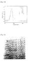
- a pattern was formed by dissolving the unexposed area in chloroform and the picture thereof was shown in Fig. 14.
- the compounds having acetylene groups can be cured by UV irradiation and a pattern thereof using a mask can be also formed.
- the organic compounds of the present invention can be used for preparing a thin film by vacuum deposition polymerization which is appropriate to negative-type photoresists.
- 1,4-di(4-ethynylphenyl)adamantine was prepared by the same procedure of Example 4 with using 5.0g (14.9mmol) of 1,4-di(4-bromophenyl)adamantine, prepared by reacting 5.0g (21.9mmol) of 1,4-diphenyladamantane and bromine, instead of N,N'-bis(3-methylphenyl)-N,N'-di(4-bromophenyl)benzidine.
- Electroluminescence device was fabricated by using a thin film formed by means of vacuum deposition polymerization of tri(4-ethynylphenyl)amine prepared from Example 3 as a hole transport layer and tris(8-hydroxyquinolinato)aluminum (Alq 3 ) as an emission layer.
- ITO glass electrode was placed into a mixture of acetone and isopropyl alcohol and washed several times with ultrasonic cleaner.
- Tri(4-ethynylphenyl)amine was deposited on the ITO electrode by a deposition chamber of Fig. 1 under 2.0 x 10 -5 torr of vacuum level and with 0.5 ⁇ /sec of rate to form a thin film having 80 ⁇ of thickness.
- a hole transport layer was prepared by polymerizing a monomer of tri(4-ethynylphenyl)amine with UV irradiation. After polymerization, an emission layer having 500 ⁇ of thickness was formed by depositing Alq 3 on the hole transport layer with a deposition chamber under 2.0 x 10 -5 torr of vacuum level and with 2.0 ⁇ /sec of rate. Thereafter, aluminum was deposited on the emission layer with a deposition chamber under 2.0 x 10 -5 torr of vacuum level and with 5.0 ⁇ /sec of rate to form a metal electrode layer having 1,500 ⁇ of thickness.
- ITO/tri(4-ethynylphenyl)amine/ Alq 3 /Al electroluminescence device Said ITO was connected with anode and said Al electrode was connected with cathode and also an operating voltage was 3.5V and an electric current was 0.5mA.
- the present invention provides an organic thin film of an organic compound having at least one acetylene group formed by deposition under the vacuum and simultaneous or then polymerization by heat treatment or UV irradiation.
- the process of the present invention does not require high temperature process and does not produce by-products.
- the thin film formed by vacuum deposition polymerization has uniform thickness and excellent thermal stability and further, be applied in various fields such as interlayer dielectric film of semiconductors, electroluminescence devices, solar cells, drum of copy machine and laser printer, and various sensors.
Landscapes
- Chemical & Material Sciences (AREA)
- Organic Chemistry (AREA)
- Engineering & Computer Science (AREA)
- Materials Engineering (AREA)
- Manufacturing & Machinery (AREA)
- Health & Medical Sciences (AREA)
- Chemical Kinetics & Catalysis (AREA)
- Medicinal Chemistry (AREA)
- Polymers & Plastics (AREA)
- Addition Polymer Or Copolymer, Post-Treatments, Or Chemical Modifications (AREA)
- Electroluminescent Light Sources (AREA)
- Organic Low-Molecular-Weight Compounds And Preparation Thereof (AREA)
- Polymerisation Methods In General (AREA)
- Pyridine Compounds (AREA)
- Indole Compounds (AREA)
- Physical Vapour Deposition (AREA)
- Heterocyclic Carbon Compounds Containing A Hetero Ring Having Nitrogen And Oxygen As The Only Ring Hetero Atoms (AREA)
- Pyrane Compounds (AREA)
- Pyrrole Compounds (AREA)
- Nitrogen And Oxygen Or Sulfur-Condensed Heterocyclic Ring Systems (AREA)
Abstract
Description
- The present invention relates to an organic compound having acetylene group(s), a thin film formed by vacuum deposition polymerization using said organic compound, vacuum deposition polymerization to form said thin film, and an electroluminescence device containing said thin film. More particularly, the present invention relates to an organic compound having at least one acetylene groups, vacuum deposition polymerization in which said organic compound is deposited on the substrate and simultaneously or then polymerized by thermal and/or UV radiation curing to form a polymer thin film, and an electroluminescence device using at least one layer of said thin film.
- Organic functional thin film is recently used in Thin Film Transistor-Liquid Crystal Device (TFT-LCD), organic polymer electroluminescence devices, piezoelectric devices, optical materials and the like because it is applicable for portable electronics. Conventional organic thin film can be prepared by wet process such as dip coating or spin coating but it has disadvantages in that a certain polymer which is insoluble in a solvent requires an additional process of coating a precursor and heating to form a thin film. Further, wet process results in problems including easy contamination by a solvent, difficulty in controlling film thickness and film uniformity below 100nm. Also wet process is not favorable for a following process such as a manufacturing process of semiconductors which requires dry process.
- On the other hand, a deposition polymerization is a method to produce an organic thin film by direct polymerization on the substrate by vaporizing a precursor with heat energy under high vacuum. Said deposition polymerization can i)produce a thin film through a simple vacuum device without using a catalyst or a solvent, ii)prevent from contamination of impurities, iii)control molecular sequences and film thickness, iv)provide easy preparing of a thin film of inprocessible polymer, and v)form a pattern by using a mask. Therefore, it is very important to develop thin film forming technology by vacuum deposition polymerization which is expected to be essential to various electronic devices in future information industries.
- There are two types of deposition polymerizations to form a thin film which are radical deposition polymerization and condensation polymerization. Radical deposition polymerization is a method to prepare a thin film on the substrate by polymerizing radicals generated by chemical reactions of precursors by thermal and/or UV radiation after vaporizing precursors. Different thin films such as poly(p-xylylene) (A. Greiner, Trends in Polymer, 5(1997), 12), poly(naphthalene) (D. W. Smith et al., J. Am. Chem. Soc., 120(1998), 9078), poly(benzocyclobutene) or poly(p-phenylenevinylene) (K. M. Vaeth et al., Macromolecules, 31(1998), 6789), and Teflon (T. C. Nason et al., Appl. Phys. Lett., 60(1992), 1866), are prepared by radical deposition polymerization. Thin films prepared by said radical deposition polymerization provide excellent thermal stability and low dielectric constant and thus, they are very attractive for applications as interlayer dielectrics of semiconductors.
- On the other hand, condensation polymerization is a method to prepare a thin film by condensation polymerization after two kinds of precursors are simultaneously deposited on the substrate. Thin films such as polyimide (Ukishima et al., Thin Solid Films, 308-309(1997), 479), polyamide (A. Kubono et al., Thin Solid Films, 289(1996), 107), and polyurea (F. Fukuda, Key Eng. Mater., 92-93(1994), 143), polyazomethane (S. Tatsuura et al., Appl. Phys. Lett., 62(1993), 2182), are prepared by condensation polymerization. Thin films prepared by said condensation polymerization provide excellent electrical and optical properties such as piezoelectricity, non-linear optical property and conductivity and thus, they call the high attention as high-functional materials.
- However, said radical deposition polymerization has to generate radicals by decomposing precursors at a high temperature over 400°C which is not suitable for the device manufacturing process. And said condensation polymerization has also disadvantages for producing by-products during condensation polymerization. Therefore, it is urgent to develop vacuum deposition polymerization which does not require thermal curing at a high temperature for decomposing precursors as well as does not produce by-products during polymerization and further, an appropriate precursor for vacuum deposition polymerization.
- An object of the present invention is to provide an organic compound having at least one acetylene group which can be easily polymerized by thermal curing at relatively low temperature or UV irradiation.
- Another object of the present invention is to provide a vacuum deposition polymerization to obtain a thin film having uniform thickness without generating by-products by using said organic compound.
- Another object of the present invention is to provide a thin film prepared by vacuum deposition polymerization having an improved thermal stability.
- Another object of the present invention is to provide an electroluminescent device fabricated by using said thin film.
-
- Fig. 1 represents a schematic view of vacuum deposition chamber for thermal and UV radiation curing.
- Fig. 2 represents a schematic view of electroluminescence device.
- Fig. 3 represents NMR spectrum of 2-ethynylfluorene.
- Fig. 4 represents DSC thermograms of 2-ethynylfluorene and 2,7-diethynylfluorene.
- Fig. 5 represents TGA thermograms of 2-ethynylfluorene and 2,7-diethynylfluorene after thermal curing.
- Fig. 6 represents IR spectra of 2-ethynylfluorene before and after thermal curing.
- Fig. 7 represents IR spectra of 2,7-diethynylfluorene before and after thermal curing.
- Fig. 8 represents changes of UV absorption spectra of 2,7-diethynylfluorene with UV irradiation.
- Fig. 9 represents NMR spectrum of tri(4-ethynylphenyl)amine.
- Fig. 10 represents DSC thermogram of tri(4-ethynylphenyl)amine.
- Fig. 11 represents TGA thermogram of tri(4-ethynylphenyl)amine after thermal curing.
- Fig. 12 represents changes of IR spectra of tri(4-ethynylphenyl)amine with UV irradiation.
- Fig. 13 represents changes of UV absorption spectra of tri(4-ethynylphenyl)amine with UV irradiation.
- Fig. 14 represents picture of a pattern formed on the thin film of tri(4-ethynylphenyl)amine by UV irradiation through photomask.
- Fig. 15 represents electrophotoluminescene spectra from ITO/ tri(4-ethynylphenyl)amine/Alq3/ Al device.
-
- The present invention is described in detail as set forth hereunder.
- Organic compounds having acetylene groups of the present invention is represented in the following
formula 1,wherein R1 is a hydrogen atom or R2 is bond or
 n is a natural number of 1 or above; and R is selected from the group consisting of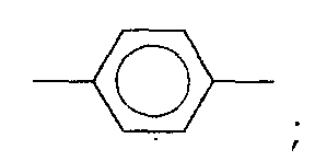





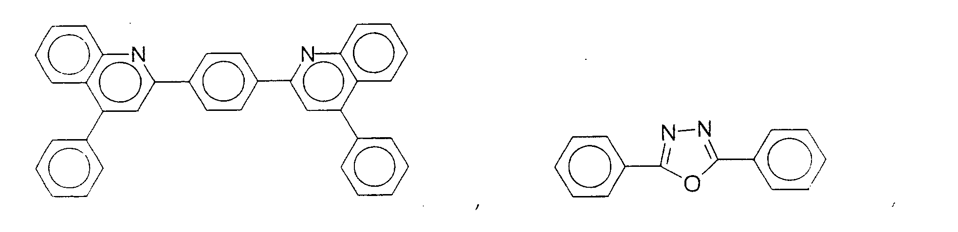

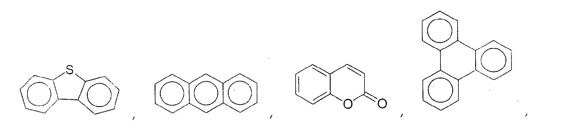
 where R' is selected from the group consisting of a hydrogen atom and C1-C12 hydrocarbons.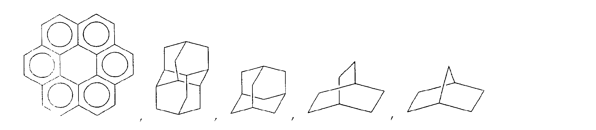
- Generally, as shown in
scheme 1, an aromatic compound having acetylene group(s) is prepared by removal of trimethylsilyl group of an aromatic compound substituted with trimethylsilyl acetylene in the presence of a base or fluoro ion where said aromatic compound substituted with trimethylsilyl acetylene is prepared by reacting aryl iodide (ArI) or aryl bromide (ArBr) with trimethylsilyl acetylene in the presence of palladium catalyst.
- Most of compounds of
formula 1 can be easily prepared from mono, di, tri, or tetra bromo (or iodo) compounds as shown inScheme 1. - Because the compound of
formula 1 having acetylene group(s) is easily cured (or polymerized) by heat treatment or UV radiation, deposition and thermal or UV radiation curing can be performed simultaneously or thermal or UV radiation curing can be performed after deposition in a process for preparing organic thin film by vacuum deposition polymerization. - Therefore, in vacuum deposition polymerization of the compound of
formula 1 to prepare a polymer thin film on the substrate such as glass or silicon wafer by using vacuum deposition chamber, said polymer thin film can be prepared by deposition and simultaneous polymerization by heat treatment or UV irradiation or by deposition and then polymerization. If necessary, thermal curing can be performed again after UV irradiation to complete polymerization. Fig. 1 represents a vacuum deposition chamber which is used for deposition polymerization. Because the vacuum deposition chamber is equipped with a heater and a UV lamp for direct heating, a thin film of an organic compound can be obtained by simultaneous deposition and polymerization or sequential deposition and polymerization. It is also possible to deposit simultaneously more than two organic compounds with this vacuum deposition chamber. - In the formation of a polymer by exposing UV light according to the present invention, pattern can be easily formed by using a mask. The only exposed area through the mask can be cured and the unexposed area is removed under the vacuum or by dissolving in a solvent so that it is possible to form the pattern wanted.
- The thin film formed by vacuum deposition polymerization of the present invention provides improved thermal stability and thus, it can be applied in various fields such as interlayer dielectrics of semiconductors, hole transport layer and emission layer of electroluminescence device, solar cells, drum of copy machine and laser printer, and various sensors.
- As shown in Fig. 2 which represents an electroluminescence device prepared by using deposition polymerized thin film, it basically includes ITO electrode, emission layer and metal electrode. Said emission layer is a thin film prepared by means of vacuum deposition polymerization of the compound of
formula 1 having at least one acetylene group. An electroluminescence device can have a hole transport layer under an emission layer. At least either a hole transport layer or an emission layer can be prepared by vacuum deposition polymerization of the present invention. And further, an electroluminescence device can, additionally, have an electron transport layer on the emission layer. Among an emission layer, a hole transport layer and an electron transport layer, at least one layer is prepared by vacuum deposition polymerization of the present invention. -

- 10g (0.06mol) of fluorene and 15.23g (0.06mol) of iodine were added into 300ml of acetic acid and stirred. 1.2ml of nitric acid and 12ml of sulfuric acid were added dropwise into the reaction mixture. After the reaction mixture was stirred 35°C for 2 h, 2L of distilled water was added to it. Unreacted fluorene was washed out with 100ml of cold acetic acid. Remaining precipitates were washed with 100ml of 5% potassium iodide solution, 100ml of 5% sodium thiosulfate solution and distilled water, successively. Washed precipitates were dried in the air and extracted by petroleum ether soxhlet. Extracted solution was cooled to obtain 7.89g (45%) of yellow needle shape 2-iodofluorene.
- Thereafter, to 150ml of triethylamine were added 7.89g of 2-iodofluorene, 379mg (0.54mmol) of bis[triphenylphosphine]palladium dichloride and 51mg (0.27mmol) of copper iodide. 4.2ml (29.7mmol) of trimethylsilylacetylene was added slowly to the reaction mixture. After the reaction was stirred for 8 h at room temperature, solvent was removed under reduced pressure. The residue was extracted with benzene and the benzene layer was washed with distilled water. The washed benzene layer was concentrated to give 6.02g (85%) of 2-trimethylsilylethynyl fluorene.
- After 6.02g (22.9mmol) of 2-trimethylsilylethynylfluorene was added to 100ml of methanol, 25ml of 1N potassium hydroxide was added dropwise thereto. The reaction mixture was stirred for 3 h at room temperature and solvent was removed under the reduced pressure. The residue was extracted with ether and the ether layer was washed with distilled water. The washed ether layer was dried over anhydrous sodium sulfate and concentrated under the reduced pressure to give crude product. The crude product was purified by column chromatography on silica gel by eluting hexane/ethylacetate(15/1) and further purified by sublimation at 60°C/2torr to give 3.71g (87%) of 2-ethynylfluorene. Fig. 3 represents NMR spectrum of the final product, 2-ethynylfluorene, and mp was measured to be 85°C.
- The DSC thermogram of 2-ethynyl fluorene as shown in Fig.4 reveals that polymerization of 2-ethynyl fluorene having one acetylene group was started at around 230°C. It indicated that deposition on the substrate and polymerization of 2-ethynylfluorene can be performed simultaneously by controlling a temperature at 230°C.
- Thermal stability of 2-ethynylfluorene after thermal curing was examined by TGA analysis and the result was shown in Fig. 5. As shown in Fig. 5, a polymer prepared by polymerizing 2-ethynylfluorene by thermal curing at 230°C under N2 was stable up to 260°C.
-

- To 100ml of propylene carbonate were added 10g (0.06mol) of fluorene and 22.43g (0.126mol) of N-bromosuccinimide (NBS). After the reaction mixture was stirred at 75°C for 6 h, 200ml of distilled water was added to obtain precipitate. The obtained precipitate was recrystallized from ethylacetate several times to give 10.89g (56%) of 2,7-dibromofluorene.
- Thereafter, to 150ml of diisopropylamine were dissolved 10.89g (33.6mmol) of 2,7-dibromofluorene obtained above, 941mg (0.67mmol) of bis[triphenylphosphine]palladium dichloride, and 128mg (0.67mmol) of copper iodide. After the reaction mixture was stirred for 2 h at room temperature, 10.45ml (73.9mmol) of trimethylsilyl acetylene was added dropwise to it. The reaction mixture was refluxed for 8 h and cooled. Solvent was removed under reduced pressure. The residue was extracted with benzene and the benzene layer was washed with distilled water. The washed benzene layer was concentrated to give 10.12g(85%) of 2,7-di(trimethylsilylethynyl)fluorene.
- Thereafter, 60ml of 1N potassium hydroxide solution was slowly added to 10.12g(28.2mmol) of 2,7-di(trimethylsilylethynyl)fluorene dissolved in 150ml of methanol. The reaction mixture was stirred for 3 h at room temperature and solvent was removed. Residue was extracted with ether and the ether layer was washed with distilled water. The washed ether layer was concentrated. The crude product was purified by column chromatography on silica gel by eluting with hexane/ethylacetate (15/1) to give 1.35g (72%) of 2,7-diethynylfluorene of which mp was 125°C.
- The DSC thermogram of 2,7-diethynylfluorene, as shown in Fig.4, reveals that polymerization of 2,7-diethynylfluorene having two acetylene groups was started at around 198°C. It indicated that deposition on the substrate and polymerization of 2,7-diethynylfluorene can be simultaneously performed by controlling a temperature around 200°C.
- Thermal stability of 2,7-diethynylfluorene after thermal curing was examined by TGA analysis as shown in Fig. 5. In Fig. 5 a polymer prepared by polymerizing 2,7-diethynylfluorene by thermal curing at 198°C for 3 h under N2 was stable up to 385°C.
- 2-Ethynylfluorene prepared from Example 1 and 2,7-diethynylfluorene prepared from Example 2 were deposited on silicon wafer by vacuum deposition chamber of Fig. 1 in order to confirm by IR spectra whether those compounds having (an) acetylene group(s) were polymerized by heat treatment. During deposition, vacuum level was 2 x 10⁻⁴ torr and deposited thickness was about 1500 Å. IR spectra of 2-ethynylfluorene and 2,7-diethynylfluorene before and after thermal curing under N2 were examined and shown in Figs. 6 and 7. Thermal curing of each 2-ethynylfluorene and 2,7-diethynylfluorene was carried out at 230°C and at 198°C, respectively, for 30 min. In Figs. 6 and 7, both 2-ethynylfluorene and 2,7-diethynylfluorene show strong peak of stretching vibration at 3283 cm-1 for ≡ C-H and a weak peak of stretching vibration at 2099 cm-1 for C ≡ C before thermal curing. After thermal curing for 30 min, both stretching peaks for ≡ C-H and C ≡ C were disappeared and a peak of stretching vibration at between 1600 and 1700 cm-1 for C=C was appeared. This indicated that after thermal curing both 2-ethynylfluorene and 2,7-diethynylfluorene having (an) acetylene group(s) were polymerized by changing a triple bond, C ≡ C, to a double bond, C=C.
- 2,7-Diethynylfluorene prepared from Example 2 was deposited on the glass using vacuum deposition chamber of Fig. 1, and was examined UV absorption spectrum during UV irradiation. During deposition, vacuum level was 2 x 10⁻⁴ torr and deposited thickness was about 300 Å. Fig. 8 represents changes of UV absorption spectra at different irradiation time. As exposure of UV light increased, the width of maximum absorption peak at 340nm was getting broader and the peak shifted toward longer wavelength. It indicated that the length of double bond was getting increased, that is, a triple bond of the compound having acetylene groups was changed into a double bond by polymerization with UV irradiation.
-
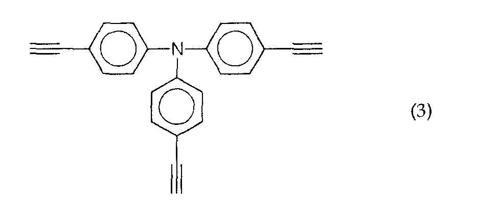
- 10g (0.0408mol) of triphenylamine was added to 150ml of chloroform with stirring. 19.54g (0.122mol) of bromine dissolved in chloroform was added to the reaction mixture and stirred for 2 h at room temperature. 400ml of hot ethanol was added to the reaction mixture and left at room temperature to produce precipitates. Said precipitates was extracted by methanol soxhlet to give 15.54g (79%) of tri(4-bromophenyl)amine
- Thereafter, to 200ml of diisopropylamine were added 15.54g (0.032mol) of tri(4-bromophenyl)amine, 1.35g (1.92mmol) of bis[triphenylphosphin]palladium dichloride and 9.43g (0.96mmol) of copper iodide. After the reaction mixture was stirred for 2 h at room temperature, 9.43g (96mmol) of trimethylsilyl acetylene was slowly added to the reaction mixture. The reaction mixture was refluxed for 8 h and cooled. Solvent was removed under the reduced pressure. The residue was extracted with benzene and the benzene layer was washed with distilled water. The washed benzene layer was concentrated to give 13.84g (81%) of tri(4-trimethylsilylethynylphenyl)amine.
- To a mixture of 180ml of tetrahydrofuran (THF) and 240ml of methanol were added 13.84g (0.026mol) of tri(4-trimethylsilylethynylphenyl)amine and 4.53g (0.078mol) of potassium fluoride. The reaction mixture was heated at 50°C for 5 h, cooled down to room temperature, and solvent was removed under the reduced pressure. The residue was extracted with ether and the ether layer was washed with distilled water. The washed ether layer was concentrated to give crude product. The crude product was purified by column chromatography on silica gel by eluting with hexane to give 6.182g (75%) of tri(4-ethynylphenyl)amine of which NMR spectrum was shown in Fig. 9 and mp was 115°C.
- The DSC thermogram of tri(4-ethynylphenyl)amine, as shown in Fig. 10, revealed that polymerization of tri(4-ethynylphenyl)amine having three acetylene groups was started at 185 °C. It indicated that deposition on the substrate and polymerization of 2,7-diethynylfluorene can be simultaneously carried out by controlling a temperature around 185°C.
- Thermal stability of tri(4-ethynylphenyl)amine after thermal curing was examined by TGA analysis and the result was shown in Fig. 11. In Fig. 11 a polymer prepared by polymerizing tri(4-ethynylphenyl)amine by thermal curing at 185 °C under N2 for 30 min was stable up to 375°C.
- Tri(4-ethynylphenyl)amine prepared from Example 3 was deposited on silicon wafer in the vacuum deposition chamber of Fig. 1 to examine by IR spectrum whether those compound having three acetylene groups was polymerized by UV irradiation. During deposition, vacuum level was 2 x 10⁻⁵ torr and deposited thickness was about 1500 Å. IR spectra of tri(4-ethynylphenyl)amine were examined during UV irradiation and shown in Fig. 12. In Fig. 12, tri(4-ethynylphenyl)amine showed a strong peak of stretching vibration at 3277 cm-1 for ≡ C-H and a weak peak of stretching vibration at 2102 cm-1 for C ≡ C before thermal curing. After thermal curing, both peaks for ≡ C-H and C ≡ C were disappeared and a peak of stretching vibration at between 1600 and 1700 cm-1 for C=C was appeared. This indicated that tri(4-ethynylphenyl)amine having three acetylene groups was polymerized with UV irradiation by changing a triple bond, C≡ C, to a double bond, C=C.
- And polymerization of tri(4-ethynylphenyl)amine with UV light was also clarified by UV absorption spectrum. During deposition, vacuum level was 2 x 10⁻⁴ torr and deposited thickness was about 300 Å. Fig. 13 showed changes of UV absorption spectra with irradiation time. As exposure time of UV light increased, the width of maximum absorption peat at 340nm was getting broader and the peak was shifted toward longer wavelength. It indicated that the length of double bond was getting increased, that is, a triple bond of the compound having acetylene group was changed to a double bond by polymerization with UV light.
- On the other hand, after exposing UV light at 254 nm or 320nm of wavelength by using a mask on the substrate of the glass deposited with tri(4-ethynylphenyl)amine, a pattern was formed by dissolving the unexposed area in chloroform and the picture thereof was shown in Fig. 14. The compounds having acetylene groups can be cured by UV irradiation and a pattern thereof using a mask can be also formed. The organic compounds of the present invention can be used for preparing a thin film by vacuum deposition polymerization which is appropriate to negative-type photoresists.
-

- To 50ml of diisopropylamine were added 3.3g (4.89mmol) of N,N-bis(3-methylphenyl)-N,N-di(4-bromophenyl)benzidine, 137mg (0.196mmol) of bis[triphenylphosphine]palladium dichloride and 18.7mg (0.098mmol) of copper iodide. After the reaction mixture was stirred for 2 h at room temperature, 0.96mg (9.78mmol) of trimethylsilylacetylene was slowly added to it. The reaction mixture was refluxed for 8 h. The solvent was removed under the reduced pressure. The residue was extracted with benzene and the benzene layer was washed with distilled water. The washed benzene layer was concentrated to dryness to give 2.705g (78%) of N,N-bis(3-methylphenyl)-N,N-di(4-trimethylsilylethynylphenyl)benzidine.
- To a mixture of 60ml of THF and 80ml of methanol were dissolved 2.705g (3.814mmol) of N,N-bis(3-methylphenyl)-N,N-di(4-trimethylsilylethynylphenyl)benzidine and 0.443g(7.628mmol) of KF. After the reaction mixture was stirred for 5 h at 50°C, it was cooled to room temperature and the solvent was removed to dryness. The residue was extracted with chloroform and the chloroform layer was washed with distilled water. The washed chloroform layer was concentrated to dryness to give crude product which was further purified by column chromatography on silica gel by eluting with hexane/ethylacetate (9/1) to give 1.852g (86%) of N,N-bis(3-methylphenyl)-N,N-di(4-ethynylphenyl)benzidine.
Elemental Analysis of N,N-bis(3-methylphenyl)-N,N-di(4-ethynylphenyl)benzidine C H N Found 89.27% 5.77% 4.94% Calculated 89.33% 5.71% 4.96% -

- 1.503g (71%) of 4-(ethynylphenyl)diphnylamine was prepared by the same procedure of Example 4 with using 3.0g (9.25mmol) of (4-bromophenyl)diphenylamine(4-bromophenyl)diphenylamine instead of N,N'-bis(3-methylphenyl)-N,N'-di(4-bromophenyl)benzidine.
Elemental Analysis of 4-(ethynylphenyl)diphenylamine C H N Found 89.16% 5.70% 5.14% Calculated 89.19% 5.61% 5.20% -
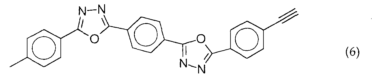
- 1.75g (65%) of 1,3-di(5-(4-ethynylphenyl)-1,3,4-oxadiazole)benzene was prepared by the same procedure of Example 4 with using 5.0g (9.54mmol) of 1,3-di(5-(4-bromophenyl)-1,3,4-oxadiazole)benzene instead of N,N'-bis(3-methylphenyl)-N,N'-di(4-bromophenyl)benzidine.
Elemental Analysis of 1,3-di(5-(4-ethynylphenyl)-1,3,4-oxadiazole)benzene C H N Found 75.29% 3.44% 13.49% Calculated 76.65% 3.41% 13.52% -

- 2.37g (65%) of 5,5-diethynyl-2,2:5,2-terthiophene was prepared by the same procedure of Example 4 with using 5.0g (12.3mmol) of 5,5-dibromo-2,2:5,2-terthiophene instead of N,N'-bis(3-methylphenyl)-N,N'-di(4-bromophenyl)benzidine.
Elemental Analysis of 5,5-diethynyl-2,2:5,2-terthiophene C H Found 64.8 % 2.76% Calculated 64.83% 2.72% -

- 2.42g (72%) of 9,10-diethynylanthracene was prepared by the same procedure of Example 4 with using 5.0g (14.9mmol) of 9,10-dibromoanthracene instead of N,N'-bis(3-methylphenyl)-N,N'-di(4-bromophenyl)benzidine.
Elemental Analysis of 9,10-diethynylanthracene C H Found 95.53% 4.47% Calculated 95.55 % 4.45 % -

- 2.63g (70%) of 1,4-di(4-ethynylphenyl)adamantine was prepared by the same procedure of Example 4 with using 5.0g (14.9mmol) of 1,4-di(4-bromophenyl)adamantine, prepared by reacting 5.0g (21.9mmol) of 1,4-diphenyladamantane and bromine, instead of N,N'-bis(3-methylphenyl)-N,N'-di(4-bromophenyl)benzidine.
Elemental Analysis of 1,4-di(4-ethynylphenyl)adamantine C H Found 92.78% 7.22% Calculated 92.81% 7.19% - Electroluminescence device was fabricated by using a thin film formed by means of vacuum deposition polymerization of tri(4-ethynylphenyl)amine prepared from Example 3 as a hole transport layer and tris(8-hydroxyquinolinato)aluminum (Alq3) as an emission layer. ITO glass electrode was placed into a mixture of acetone and isopropyl alcohol and washed several times with ultrasonic cleaner. Tri(4-ethynylphenyl)amine was deposited on the ITO electrode by a deposition chamber of Fig. 1 under 2.0 x 10⁻⁵ torr of vacuum level and with 0.5 Å /sec of rate to form a thin film having 80 Å of thickness. During deposition, a hole transport layer was prepared by polymerizing a monomer of tri(4-ethynylphenyl)amine with UV irradiation. After polymerization, an emission layer having 500 Å of thickness was formed by depositing Alq3 on the hole transport layer with a deposition chamber under 2.0 x 10⁻⁵ torr of vacuum level and with 2.0 Å /sec of rate. Thereafter, aluminum was deposited on the emission layer with a deposition chamber under 2.0 x 10⁻⁵ torr of vacuum level and with 5.0 Å /sec of rate to form a metal electrode layer having 1,500 Å of thickness. Fig. 5 showed an electroluminescence spectra of ITO/tri(4-ethynylphenyl)amine/ Alq3/Al electroluminescence device. Said ITO was connected with anode and said Al electrode was connected with cathode and also an operating voltage was 3.5V and an electric current was 0.5mA.
- As described above in detail, the present invention provides an organic thin film of an organic compound having at least one acetylene group formed by deposition under the vacuum and simultaneous or then polymerization by heat treatment or UV irradiation. The process of the present invention does not require high temperature process and does not produce by-products. The thin film formed by vacuum deposition polymerization has uniform thickness and excellent thermal stability and further, be applied in various fields such as interlayer dielectric film of semiconductors, electroluminescence devices, solar cells, drum of copy machine and laser printer, and various sensors.
Claims (9)
- An organic compound having acetylene group expressed in formula 1,wherein
 R1 is a hydrogen atom or
 R2 is bond or
 n is a natural number of 1 or above; andR is selected from the group consisting of




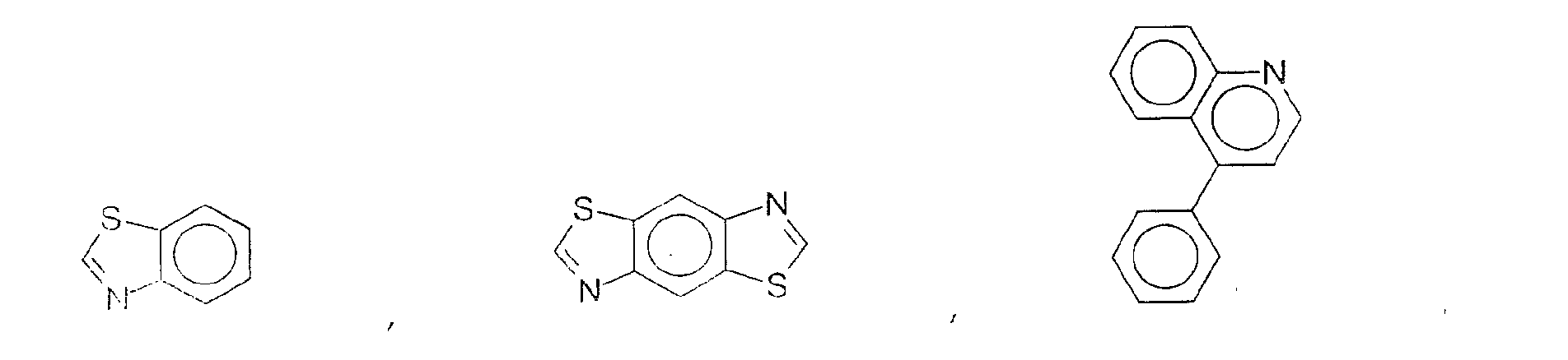


 where R' is selected from the group consisting of a hydrogen atom and C1-C12 hydrocarbons.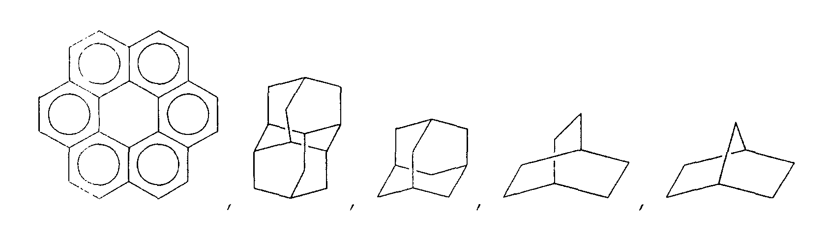
- A vacuum deposition polymerization in which at least one of said organic compounds of claim 1 is/are deposited on the substrate and simultaneously or then polymerized by heat treatment and/or UV irradiation to form a polymer thin film.
- The vacuum deposition polymerization according to claim 2, wherein additional thermal curing is performed after said UV irradiation.
- The vacuum deposition polymerization according to claims 2 and 3, wherein said UV light is exposed through a patterned photo mask to form pattern by removing an unexposed area.
- A thin film formed by depositing at least one of said organic compound having acetylene group of claim 1 on the substrate under vacuum and simultaneously or then polymerizing by means of heat treatment or UV irradiation.
- The thin film according to claim 5, wherein an additional thermal curing is performed after said UV irradiation.
- An electroluminescence device comprising ITO electrode layer, emission layer and metal electrode layer, wherein said emission layer is a thin film formed by depositing at least one of said organic compounds of claim 1 on the substrate and simultaneously or then polymerizing by heat treatment and/or UV irradiation.
- An electroluminescence device comprising ITO electrode layer, hole transport layer, emission layer and metal electrode layer, wherein at least one of said hole transport layer and said emission layer is/are thin film(s) formed by depositing at least one of said organic compounds of claim 1 on the substrate and simultaneously or then polymerizing by heat treatment or UV irradiation.
- An electroluminescence device comprising ITO electrode layer, hole transport layer, emission layer, electron transport layer and metal electrode layer, wherein at least one of said hole transport layer, said emission layer and said electron transport layer is/are thin film(s) formed by depositing at least one of said organic compounds of claim 1 on the substrate and simultaneously or then polymerizing by heat treatment or UV irradiation.
Applications Claiming Priority (2)
| Application Number | Priority Date | Filing Date | Title |
|---|---|---|---|
| KR1020000037784A KR100360308B1 (en) | 2000-07-03 | 2000-07-03 | Organic compounds comprising acetylene group, Vacuum deposition polymerization method using the compounds, Thin film prepared by the method, and Electroluminous element employing the film |
| KR2000037784 | 2000-07-03 |
Publications (2)
| Publication Number | Publication Date |
|---|---|
| EP1170273A1 true EP1170273A1 (en) | 2002-01-09 |
| EP1170273B1 EP1170273B1 (en) | 2003-05-28 |
Family
ID=19675953
Family Applications (1)
| Application Number | Title | Priority Date | Filing Date |
|---|---|---|---|
| EP01100286A Expired - Lifetime EP1170273B1 (en) | 2000-07-03 | 2001-01-04 | Alkynic compounds, their use as monomers in vacuum deposition polymerisation, thin films formed from these polymers and their use in electroluminescent devices |
Country Status (5)
| Country | Link |
|---|---|
| US (1) | US6682782B2 (en) |
| EP (1) | EP1170273B1 (en) |
| JP (1) | JP2002069013A (en) |
| KR (1) | KR100360308B1 (en) |
| DE (1) | DE60100307T2 (en) |
Cited By (8)
| Publication number | Priority date | Publication date | Assignee | Title |
|---|---|---|---|---|
| WO2004003102A3 (en) * | 2002-07-01 | 2004-08-26 | Merck Patent Gmbh | Polymerizable, luminescent compounds and mixtures, luminescent polymer materials and their use |
| EP1388548A3 (en) * | 2002-08-06 | 2004-09-08 | Matsushita Electric Industrial Co., Ltd. | Interlayer insulating film, method for forming the same and polymer composition |
| WO2004096783A1 (en) * | 2003-04-15 | 2004-11-11 | 3M Innovative Properties Company | Ethynyl containing electron transport agents and their use in organic luminescent devices |
| US7271406B2 (en) | 2003-04-15 | 2007-09-18 | 3M Innovative Properties Company | Electron transport agents for organic electronic devices |
| US7282275B2 (en) | 2002-04-19 | 2007-10-16 | 3M Innovative Properties Company | Materials for organic electronic devices |
| EP1537187A4 (en) * | 2002-09-05 | 2008-03-05 | Nanosys Inc | Transfer of Charge to or from Nanostructures to Perfecting Organic Species |
| US7572393B2 (en) | 2002-09-05 | 2009-08-11 | Nanosys Inc. | Organic species that facilitate charge transfer to or from nanostructures |
| CN114315608A (en) * | 2022-01-07 | 2022-04-12 | 大连理工大学盘锦产业技术研究院 | A kind of method for preparing tris (4-ethynyl phenyl) amine from triphenylamine |
Families Citing this family (39)
| Publication number | Priority date | Publication date | Assignee | Title |
|---|---|---|---|---|
| KR20010104215A (en) * | 2000-05-12 | 2001-11-24 | 야마자끼 순페이 | A method of manufacturing a light emitting device |
| SG2009086778A (en) * | 2000-12-28 | 2016-11-29 | Semiconductor Energy Lab Co Ltd | Luminescent device |
| TW545080B (en) * | 2000-12-28 | 2003-08-01 | Semiconductor Energy Lab | Light emitting device and method of manufacturing the same |
| TW518909B (en) * | 2001-01-17 | 2003-01-21 | Semiconductor Energy Lab | Luminescent device and method of manufacturing same |
| TW519770B (en) * | 2001-01-18 | 2003-02-01 | Semiconductor Energy Lab | Light emitting device and manufacturing method thereof |
| US20020139303A1 (en) * | 2001-02-01 | 2002-10-03 | Shunpei Yamazaki | Deposition apparatus and deposition method |
| SG118110A1 (en) | 2001-02-01 | 2006-01-27 | Semiconductor Energy Lab | Organic light emitting element and display device using the element |
| US20030010288A1 (en) * | 2001-02-08 | 2003-01-16 | Shunpei Yamazaki | Film formation apparatus and film formation method |
| TW582121B (en) * | 2001-02-08 | 2004-04-01 | Semiconductor Energy Lab | Light emitting device |
| US7432116B2 (en) * | 2001-02-21 | 2008-10-07 | Semiconductor Energy Laboratory Co., Ltd. | Method and apparatus for film deposition |
| SG118118A1 (en) * | 2001-02-22 | 2006-01-27 | Semiconductor Energy Lab | Organic light emitting device and display using the same |
| JP2003137933A (en) * | 2001-11-01 | 2003-05-14 | Nichia Chem Ind Ltd | Polyacetylene having thiophene ring in side chain and organic electroluminescent device using the same |
| US20030143332A1 (en) * | 2002-01-31 | 2003-07-31 | Sumitomo Chemical Company, Limited | Coating solution for forming insulating film |
| US6931132B2 (en) * | 2002-05-10 | 2005-08-16 | Harris Corporation | Secure wireless local or metropolitan area network and related methods |
| JP2004071777A (en) * | 2002-08-06 | 2004-03-04 | Fujitsu Ltd | Method for manufacturing organic insulating film, method for manufacturing semiconductor device, and method for manufacturing TFT substrate |
| KR100694364B1 (en) * | 2002-09-03 | 2007-03-12 | 캠브리지 디스플레이 테크놀로지 리미티드 | Optical devices |
| JP2004103401A (en) * | 2002-09-10 | 2004-04-02 | Konica Minolta Holdings Inc | Device and method for manufacturing the device |
| JP4637830B2 (en) * | 2003-04-02 | 2011-02-23 | ダウ グローバル テクノロジーズ インコーポレイティド | Multifunctional, substituted monomers and polyarylene compositions thereof |
| US7092206B2 (en) * | 2003-06-25 | 2006-08-15 | Hitachi Global Storage Technologies Netherlands B.V. | Magnetic head with magnetic layers of differing widths and third pole with reduced thickness |
| CN1738069A (en) * | 2004-08-17 | 2006-02-22 | 国际商业机器公司 | Electronic device manufacturing method and electronic device whose electrodes have enhanced injection characteristics |
| JP2006339049A (en) * | 2005-06-02 | 2006-12-14 | Tokki Corp | Sealing film forming device |
| WO2007043748A1 (en) * | 2005-10-14 | 2007-04-19 | Lg Life Sciences, Ltd. | Method of manufacturing plastic substrate using plasma process and plastic substrate manufactured using the method |
| KR101481933B1 (en) * | 2005-12-29 | 2015-01-14 | 쓰리엠 이노베이티브 프로퍼티즈 컴파니 | Method for atomizing material for coating processes |
| US20070190235A1 (en) * | 2006-02-10 | 2007-08-16 | Semiconductor Energy Laboratory Co., Ltd. | Film forming apparatus, film forming method, and manufacturing method of light emitting element |
| JP2007257897A (en) * | 2006-03-20 | 2007-10-04 | Seiko Epson Corp | LIGHT EMITTING DEVICE MANUFACTURING METHOD, LIGHT EMITTING DEVICE MANUFACTURING METHOD, AND ELECTRONIC DEVICE MANUFACTURING METHOD |
| DE102007017743A1 (en) * | 2007-04-12 | 2008-10-16 | Friedrich-Schiller-Universität Jena | New substituted 4,4'-diethinyltriphenylamine polymers useful as photoactive material in polymer photovoltaic cells, photodiodes, photodetectors and photosensors |
| JP2009170138A (en) * | 2008-01-11 | 2009-07-30 | Sony Corp | Display device manufacturing method, display device manufacturing composition, and display device |
| JP5297046B2 (en) * | 2008-01-16 | 2013-09-25 | キヤノントッキ株式会社 | Deposition equipment |
| WO2009093537A1 (en) | 2008-01-25 | 2009-07-30 | Nippon Chemical Works Co., Ltd. | Fluorescent agent having ethynyl group |
| US9401493B2 (en) | 2010-01-26 | 2016-07-26 | Unified Innovative Technology, Llc | Organic electroluminescent element, method for manufacturing same, and organic electroluminescent display device |
| WO2012005045A1 (en) * | 2010-07-06 | 2012-01-12 | シャープ株式会社 | Illumination device and manufacturing method thereof |
| KR101504443B1 (en) * | 2010-10-20 | 2015-03-19 | 가부시키가이샤 알박 | Apparatus for organic film formation and method for organic film formation |
| KR20130089039A (en) | 2012-02-01 | 2013-08-09 | 삼성디스플레이 주식회사 | Deposition source, deposition apparatus and method of manufacturing organic light emitting display apparatus |
| US9163307B2 (en) * | 2012-03-27 | 2015-10-20 | Massachusetts Institute Of Technology | Three-dimensional photoresists via functionalization of polymer thin films fabricated by iCVD |
| KR102052075B1 (en) | 2013-03-28 | 2020-01-09 | 삼성디스플레이 주식회사 | Deposition apparatus, method for forming thin film using the same, organic light emitting display apparatus and method for manufacturing the same |
| DE102014112038B4 (en) * | 2014-08-22 | 2018-06-14 | Fraunhofer-Gesellschaft zur Förderung der angewandten Forschung e.V. | Organic electronic component having a crosslinked organic-electronic functional layer and alkynyl ethers which can be used for producing this component |
| WO2016204022A1 (en) * | 2015-06-16 | 2016-12-22 | 株式会社アルバック | Film forming method and film forming device |
| US10115586B2 (en) * | 2016-05-08 | 2018-10-30 | Tokyo Electron Limited | Method for depositing a planarization layer using polymerization chemical vapor deposition |
| KR102296794B1 (en) * | 2016-07-28 | 2021-08-31 | 삼성에스디아이 주식회사 | Polymer, organic layer composition, and method of forming patterns |
Family Cites Families (5)
| Publication number | Priority date | Publication date | Assignee | Title |
|---|---|---|---|---|
| US4258079A (en) * | 1979-12-13 | 1981-03-24 | International Business Machines Corporation | Preparation of continuous films of diacetylenic polymers |
| JP2980521B2 (en) * | 1994-07-08 | 1999-11-22 | 三菱電機株式会社 | Organic thin film material and method for producing the same |
| EP0950254A4 (en) * | 1996-12-23 | 2002-11-27 | Univ Princeton | LUMINESCENT ORGANIC DEVICE CONTAINING A PROTECTIVE LAYER |
| KR0176336B1 (en) * | 1996-12-31 | 1999-04-01 | 박원훈 | Floren-based Alternating Copolymer Containing Acetylene Group and Electroluminescent Device Using the Same |
| KR100245841B1 (en) * | 1997-12-29 | 2000-03-02 | 박호군 | Floren composite hybrid copolymer containing multiple luminophores and electroluminescent device using same |
-
2000
- 2000-07-03 KR KR1020000037784A patent/KR100360308B1/en not_active Expired - Fee Related
-
2001
- 2001-01-03 US US09/752,555 patent/US6682782B2/en not_active Expired - Fee Related
- 2001-01-04 DE DE60100307T patent/DE60100307T2/en not_active Expired - Fee Related
- 2001-01-04 EP EP01100286A patent/EP1170273B1/en not_active Expired - Lifetime
- 2001-06-07 JP JP2001171926A patent/JP2002069013A/en active Pending
Non-Patent Citations (4)
| Title |
|---|
| "The Merck Index (12th edition)", 1996, MERCK & CO, WHITEHOUSE STATION, XP002178237 * |
| H. TANI ET AL: "Oligomers and Polymers Containing Triple Bonds. I. Derivatives of Ethynylbiphenyl and Ethynylfluorene", BULLETIN OF THE CHEMICAL SOCIETY OF JAPAN., vol. 36, no. 4, April 1963 (1963-04-01), JAPAN PUBLICATIONS TRADING CO. TOKYO., JP, pages 391 - 396, XP002178234, ISSN: 0009-2673 * |
| J. LEWIS ET AL: "Synthesis and characterisation of new acetylide-functionalised oligothiophenes and their dinuclear platinum complexes", JOURNAL OF THE CHEMICAL SOCIETY, DALTON TRANSACTIONS., 1997, CHEMICAL SOCIETY. LETCHWORTH., GB, pages 4283 - 4288, XP002178235, ISSN: 1472-7773 * |
| R. SKOWRONSKI ET AL: "Hydrocarbures benzéniques et anthracéniques à chaines latérales insaturées", BULLETIN DE LA SOCIETE CHIMIQUE DE FRANCE., no. 11, 1967, SOCIETE FRANCAISE DE CHIMIE. PARIS., FR, pages 4235 - 4243, XP002178236, ISSN: 0037-8968 * |
Cited By (17)
| Publication number | Priority date | Publication date | Assignee | Title |
|---|---|---|---|---|
| US7282275B2 (en) | 2002-04-19 | 2007-10-16 | 3M Innovative Properties Company | Materials for organic electronic devices |
| WO2004003102A3 (en) * | 2002-07-01 | 2004-08-26 | Merck Patent Gmbh | Polymerizable, luminescent compounds and mixtures, luminescent polymer materials and their use |
| EP1388548A3 (en) * | 2002-08-06 | 2004-09-08 | Matsushita Electric Industrial Co., Ltd. | Interlayer insulating film, method for forming the same and polymer composition |
| US7960489B2 (en) * | 2002-08-06 | 2011-06-14 | Panasonic Corporation | Interlayer insulating film, method for forming the same and polymer compositon |
| CN1310322C (en) * | 2002-08-06 | 2007-04-11 | 松下电器产业株式会社 | Layer insulated film and its forming method and polymer composition |
| US7232874B2 (en) * | 2002-08-06 | 2007-06-19 | Matsushita Electric Industrial Co., Ltd. | Interlayer insulating film, method for forming the same and polymer composition |
| EP1537187A4 (en) * | 2002-09-05 | 2008-03-05 | Nanosys Inc | Transfer of Charge to or from Nanostructures to Perfecting Organic Species |
| US7438833B2 (en) | 2002-09-05 | 2008-10-21 | Nanosys, Inc. | Organic species that facilitate charge transfer to or from nanostructures |
| US7572393B2 (en) | 2002-09-05 | 2009-08-11 | Nanosys Inc. | Organic species that facilitate charge transfer to or from nanostructures |
| US7572395B2 (en) | 2002-09-05 | 2009-08-11 | Nanosys, Inc | Organic species that facilitate charge transfer to or from nanostructures |
| US7943064B2 (en) | 2002-09-05 | 2011-05-17 | Nanosys, Inc. | Organic species that facilitate charge transfer to or from nanostructures |
| US8562867B2 (en) | 2002-09-05 | 2013-10-22 | Nanosys, Inc. | Organic species that facilitate charge transfer to or from nanostructures |
| US7271406B2 (en) | 2003-04-15 | 2007-09-18 | 3M Innovative Properties Company | Electron transport agents for organic electronic devices |
| US7192657B2 (en) | 2003-04-15 | 2007-03-20 | 3M Innovative Properties Company | Ethynyl containing electron transport dyes and compositions |
| WO2004096783A1 (en) * | 2003-04-15 | 2004-11-11 | 3M Innovative Properties Company | Ethynyl containing electron transport agents and their use in organic luminescent devices |
| CN114315608A (en) * | 2022-01-07 | 2022-04-12 | 大连理工大学盘锦产业技术研究院 | A kind of method for preparing tris (4-ethynyl phenyl) amine from triphenylamine |
| CN114315608B (en) * | 2022-01-07 | 2024-05-28 | 大连理工大学盘锦产业技术研究院 | A method for preparing tri(4-ethynylphenyl)amine from triphenylamine |
Also Published As
| Publication number | Publication date |
|---|---|
| DE60100307T2 (en) | 2004-04-29 |
| DE60100307D1 (en) | 2003-07-03 |
| EP1170273B1 (en) | 2003-05-28 |
| JP2002069013A (en) | 2002-03-08 |
| KR20020003770A (en) | 2002-01-15 |
| US20020018912A1 (en) | 2002-02-14 |
| KR100360308B1 (en) | 2002-11-18 |
| US6682782B2 (en) | 2004-01-27 |
Similar Documents
| Publication | Publication Date | Title |
|---|---|---|
| US6682782B2 (en) | Organic compound having an acetylene group, vacuum deposition polymerization thereof, deposited polymerized thin film, and electroluminescence device containing same | |
| TWI642675B (en) | Coating composition and organic light emitting device | |
| JP5274745B2 (en) | Materials that can be structured, methods of manufacturing the same, and uses thereof | |
| CN1330614C (en) | Diphenyl anthracene derivate and organic electroluminescent apparatus using diphenyl anthracene derivate | |
| Bacher et al. | Photo-cross-linked triphenylenes as novel insoluble hole transport materials in organic LEDs | |
| CN100508237C (en) | Electronic devices comprising an organic conductor and semiconductor as well as an intermediate buffer layer made of a crosslinked polymer | |
| JP4714153B2 (en) | Crosslinkable substituted fluorene compounds | |
| EP0449125B1 (en) | Thin film electroluminescence device and process for production thereof | |
| KR101711402B1 (en) | Organic electroluminescent device | |
| US5929194A (en) | Crosslinkable or chain extendable polyarylpolyamines and films thereof | |
| US6355773B1 (en) | Functional polymer and organic electroluminescence element, optical memory, and hole transport element using the same | |
| CN101903345A (en) | Hole Transport Polymers for Electronic Devices | |
| JP3643433B2 (en) | Triphenylamine-containing polyetherketone, process for producing the same, and organic EL device using the same | |
| Magaldi et al. | Hole transporting materials for perovskite solar cells: molecular versus polymeric carbazole-based derivatives | |
| CN108912329A (en) | Preparation method and application of patterned two-dimensional conjugated microporous polymer | |
| CN106575719B (en) | Organic electronic components with cross-linked organic electronic functional layers and alkyne ethers useful for the manufacture of the components | |
| JP3939533B2 (en) | Electroluminescent polymer introduced with fluorene and electroluminescent device using the same | |
| CN117924671A (en) | Polymer semiconductor material containing benzene or pyridine ethynyl triphenylamine, hole transport material formed by crosslinking of polymer semiconductor material and application of hole transport material | |
| CN113861050B (en) | Photosensitive compound, anti-solvent type hole transport layer material prepared from photosensitive compound and application of photosensitive compound | |
| KR102735402B1 (en) | Highly fluorinated polymer photoresist containing Si atoms and method for manufacturing organic electronic device using the same | |
| Usluer | New spirobifluorene-based hole-transporting semiconductors for electroluminescent devices | |
| US7659009B2 (en) | Thermally crosslinkable materials and multi-layered devices therefrom | |
| CN115716787B (en) | An alkyl fluorene small molecule compound and its preparation method and application | |
| KR102329345B1 (en) | Compounds comprising benzophenone group, Organic electronic device comprising organic layers comprising the photo-cured of the monomer compounds | |
| WO2006001874A1 (en) | Linear polysiloxanes, silicone composition, and organic light-emitting diode |
Legal Events
| Date | Code | Title | Description |
|---|---|---|---|
| PUAI | Public reference made under article 153(3) epc to a published international application that has entered the european phase |
Free format text: ORIGINAL CODE: 0009012 |
|
| AK | Designated contracting states |
Kind code of ref document: A1 Designated state(s): DE ES FR GB IT Kind code of ref document: A1 Designated state(s): AT BE CH CY DE DK ES FI FR GB GR IE IT LI LU MC NL PT SE TR |
|
| AX | Request for extension of the european patent |
Free format text: AL;LT;LV;MK;RO;SI |
|
| 17P | Request for examination filed |
Effective date: 20020123 |
|
| 17Q | First examination report despatched |
Effective date: 20020524 |
|
| AKX | Designation fees paid |
Free format text: DE ES FR GB IT |
|
| GRAH | Despatch of communication of intention to grant a patent |
Free format text: ORIGINAL CODE: EPIDOS IGRA |
|
| RIC1 | Information provided on ipc code assigned before grant |
Free format text: 7C 08F 38/00 A, 7H 05B 33/02 B |
|
| GRAH | Despatch of communication of intention to grant a patent |
Free format text: ORIGINAL CODE: EPIDOS IGRA |
|
| GRAA | (expected) grant |
Free format text: ORIGINAL CODE: 0009210 |
|
| AK | Designated contracting states |
Designated state(s): DE ES FR GB IT |
|
| PG25 | Lapsed in a contracting state [announced via postgrant information from national office to epo] |
Ref country code: IT Free format text: LAPSE BECAUSE OF FAILURE TO SUBMIT A TRANSLATION OF THE DESCRIPTION OR TO PAY THE FEE WITHIN THE PRESCRIBED TIME-LIMIT;WARNING: LAPSES OF ITALIAN PATENTS WITH EFFECTIVE DATE BEFORE 2007 MAY HAVE OCCURRED AT ANY TIME BEFORE 2007. THE CORRECT EFFECTIVE DATE MAY BE DIFFERENT FROM THE ONE RECORDED. Effective date: 20030528 |
|
| REG | Reference to a national code |
Ref country code: GB Ref legal event code: FG4D |
|
| REG | Reference to a national code |
Ref country code: IE Ref legal event code: FG4D |
|
| REF | Corresponds to: |
Ref document number: 60100307 Country of ref document: DE Date of ref document: 20030703 Kind code of ref document: P |
|
| PG25 | Lapsed in a contracting state [announced via postgrant information from national office to epo] |
Ref country code: ES Free format text: LAPSE BECAUSE OF FAILURE TO SUBMIT A TRANSLATION OF THE DESCRIPTION OR TO PAY THE FEE WITHIN THE PRESCRIBED TIME-LIMIT Effective date: 20030908 |
|
| ET | Fr: translation filed | ||
| PLBE | No opposition filed within time limit |
Free format text: ORIGINAL CODE: 0009261 |
|
| STAA | Information on the status of an ep patent application or granted ep patent |
Free format text: STATUS: NO OPPOSITION FILED WITHIN TIME LIMIT |
|
| 26N | No opposition filed |
Effective date: 20040302 |
|
| REG | Reference to a national code |
Ref country code: IE Ref legal event code: MM4A |
|
| PGFP | Annual fee paid to national office [announced via postgrant information from national office to epo] |
Ref country code: DE Payment date: 20061229 Year of fee payment: 7 |
|
| PGFP | Annual fee paid to national office [announced via postgrant information from national office to epo] |
Ref country code: GB Payment date: 20070103 Year of fee payment: 7 |
|
| PGFP | Annual fee paid to national office [announced via postgrant information from national office to epo] |
Ref country code: FR Payment date: 20070109 Year of fee payment: 7 |
|
| GBPC | Gb: european patent ceased through non-payment of renewal fee |
Effective date: 20080104 |
|
| PG25 | Lapsed in a contracting state [announced via postgrant information from national office to epo] |
Ref country code: DE Free format text: LAPSE BECAUSE OF NON-PAYMENT OF DUE FEES Effective date: 20080801 |
|
| REG | Reference to a national code |
Ref country code: FR Ref legal event code: ST Effective date: 20081029 |
|
| PG25 | Lapsed in a contracting state [announced via postgrant information from national office to epo] |
Ref country code: GB Free format text: LAPSE BECAUSE OF NON-PAYMENT OF DUE FEES Effective date: 20080104 |
|
| PG25 | Lapsed in a contracting state [announced via postgrant information from national office to epo] |
Ref country code: FR Free format text: LAPSE BECAUSE OF NON-PAYMENT OF DUE FEES Effective date: 20080131 |