EP1168645A2 - Transmitter-receiver circuit - Google Patents
Transmitter-receiver circuit Download PDFInfo
- Publication number
- EP1168645A2 EP1168645A2 EP01109681A EP01109681A EP1168645A2 EP 1168645 A2 EP1168645 A2 EP 1168645A2 EP 01109681 A EP01109681 A EP 01109681A EP 01109681 A EP01109681 A EP 01109681A EP 1168645 A2 EP1168645 A2 EP 1168645A2
- Authority
- EP
- European Patent Office
- Prior art keywords
- voltage
- components
- control logic
- transmit
- supply voltage
- Prior art date
- Legal status (The legal status is an assumption and is not a legal conclusion. Google has not performed a legal analysis and makes no representation as to the accuracy of the status listed.)
- Granted
Links
Images


Classifications
-
- H—ELECTRICITY
- H04—ELECTRIC COMMUNICATION TECHNIQUE
- H04B—TRANSMISSION
- H04B1/00—Details of transmission systems, not covered by a single one of groups H04B3/00 - H04B13/00; Details of transmission systems not characterised by the medium used for transmission
- H04B1/38—Transceivers, i.e. devices in which transmitter and receiver form a structural unit and in which at least one part is used for functions of transmitting and receiving
- H04B1/40—Circuits
-
- H—ELECTRICITY
- H04—ELECTRIC COMMUNICATION TECHNIQUE
- H04B—TRANSMISSION
- H04B1/00—Details of transmission systems, not covered by a single one of groups H04B3/00 - H04B13/00; Details of transmission systems not characterised by the medium used for transmission
- H04B1/06—Receivers
- H04B1/16—Circuits
- H04B1/1607—Supply circuits
- H04B1/1615—Switching on; Switching off, e.g. remotely
-
- H—ELECTRICITY
- H04—ELECTRIC COMMUNICATION TECHNIQUE
- H04W—WIRELESS COMMUNICATION NETWORKS
- H04W52/00—Power management, e.g. TPC [Transmission Power Control], power saving or power classes
- H04W52/02—Power saving arrangements
- H04W52/0209—Power saving arrangements in terminal devices
- H04W52/0261—Power saving arrangements in terminal devices managing power supply demand, e.g. depending on battery level
- H04W52/0274—Power saving arrangements in terminal devices managing power supply demand, e.g. depending on battery level by switching on or off the equipment or parts thereof
- H04W52/028—Power saving arrangements in terminal devices managing power supply demand, e.g. depending on battery level by switching on or off the equipment or parts thereof switching on or off only a part of the equipment circuit blocks
-
- Y—GENERAL TAGGING OF NEW TECHNOLOGICAL DEVELOPMENTS; GENERAL TAGGING OF CROSS-SECTIONAL TECHNOLOGIES SPANNING OVER SEVERAL SECTIONS OF THE IPC; TECHNICAL SUBJECTS COVERED BY FORMER USPC CROSS-REFERENCE ART COLLECTIONS [XRACs] AND DIGESTS
- Y02—TECHNOLOGIES OR APPLICATIONS FOR MITIGATION OR ADAPTATION AGAINST CLIMATE CHANGE
- Y02D—CLIMATE CHANGE MITIGATION TECHNOLOGIES IN INFORMATION AND COMMUNICATION TECHNOLOGIES [ICT], I.E. INFORMATION AND COMMUNICATION TECHNOLOGIES AIMING AT THE REDUCTION OF THEIR OWN ENERGY USE
- Y02D30/00—Reducing energy consumption in communication networks
- Y02D30/70—Reducing energy consumption in communication networks in wireless communication networks
Definitions
- the present invention relates to transmission / reception circuits and in particular to transmission / reception circuits for cordless telephones, data transmission devices such as e.g. Data transmission devices of the DECT and Bluetooth standards, mobile phones, such as GSM, DCS, PCS mobile phones, and ISM band data transfers.
- data transmission devices such as e.g. Data transmission devices of the DECT and Bluetooth standards
- mobile phones such as GSM, DCS, PCS mobile phones, and ISM band data transfers.
- the power consumption during operation of the transmission / reception circuit is reduced by using entire systems, which comprise several blocks, e.g. Send or receive path, included, switched on or off or put into a standby mode.
- entire systems which comprise several blocks, e.g. Send or receive path, included, switched on or off or put into a standby mode.
- a mixer, an intermediate frequency amplifier and a frequency modulation detection circuit or an FM detector can be deactivated during transmission.
- a transmission output stage and a preamplifier can be switched off during a reception process.
- the synthesizer or the frequency generation circuit is required both during the transmission and the reception process and can consequently only be put into a standby (standby) operating state if neither transmission nor reception is carried out.
- some currently available transmission / reception circuits have a continuous, dynamic control of the amplification of the intermediate frequency amplifier and of the transmission output stage, which are dynamically regulated during operation.
- RSSI Receive Signal Strength Indicator
- AGC Automatic Gain Control
- a disadvantage of the existing transmit / receive systems is that many function blocks are oversized for the actual tasks during operation and consequently require too much power loss. The reason for this is that the individual components must be designed for the worst reception and transmission conditions, i.e. for the "worst case" case with maximum adjacent channel interference and minimal reception power.
- the received signal strength can vary, for example, between -94 dBm and +10 dBm, with the received power minimum value of -94 dBm being reached only in the rarest of cases.
- the adjacent channel interferers rarely reach the maximum values specified in the specifications, if they exist at all.
- the object of the present invention is one To create transmit / receive circuit in which the operating power consumption is lower.
- a transmission / reception circuit has a plurality of electronic components which are connected in order to cooperate for the transmission and reception of data, the components being controllable by control signals.
- the transmit / receive circuit also has control logic, which is connected to the plurality of electronic components, for monitoring current operating parameters of the transmit / receive circuit and for outputting control signals to the plurality of electronic components depending on the current operating parameters, the control signals being at the components comprise at least two parameters from a group of parameters consisting of the supply voltage, the amplification, a filter selection and a clock speed with which at least one of the components is operated.
- a transmission / reception circuit comprises a transmission part, a reception part and a synthesizer circuit or frequency generation circuit.
- the control logic controls a plurality of voltage regulators via voltage signals depending on the received signal strength or similar signals, such as, for example, battery charge status information, received signal interference information and signals from a baseband processor, which are connected to corresponding electronic components of the transmit / receive circuit.
- the transmit / receive circuit further comprises a plurality of intermediate frequency filters, from which the control logic can select a filter which is adapted to the current operating parameters and which, on the one hand, has a sufficiently narrow frequency bandwidth and, on the other hand, the lowest possible insertion loss.
- the signal / receive circuit uses the received signal strength as the current operating parameters, Battery level information, receive signal interference information, and signals from a baseband processor, indicating whether there is a transmit or receive operation to control the electronic components such that the supply voltage and gain reduce in response to an increase in input signal strength, the supply voltage and gain in response a decrease in the battery state of charge is further reduced, a filter with a lower insertion loss and a wider pass frequency band is selected when reception signal interference decreases, and the clock speed is reduced in response to a decrease in the data rate transmission rate.
- Voltage regulators such as linear and switching regulators are used to control the amplification and the supply voltage.
- An advantage of the present invention is that by using the current operating parameters, e.g. the reception conditions or the battery charge state, an adapted operating state of the transmission / reception circuit can be ensured.
- the individual subsystems e.g. activate or deactivate the transmission or reception path, or only dynamically regulate the intermediate frequency amplifier or the transmission output stage, in the present invention, through the dynamic control, configuration and supply of individual components in accordance with the current operating parameters during operation, a highly efficient, performance-optimized operation of the total transmission / reception circuit achieved.
- the separate power supply of the individual electronic components of the circuit by means of the various voltage regulators ensures that all components are decoupled.
- strong changes in load such as the switching on or off of one or more components, do not have the effect of a fluctuation in the supply voltage, as is the case when the electronic Components would be connected directly to the same power supply.
- the voltage regulators can be used to place the electronic components in a standby mode, in which no supply voltage is supplied to the electronic components, and consequently leakage currents are avoided, and the voltage regulators themselves require a minimal supply current. In this way, the operating time of a battery-operated transceiver unit can be extended.
- the transmission / reception circuit which intelligently, dynamically supplies, controls and configures the individual electronic components, (a) the operating time of a battery-operated transmitting / receiving unit can be extended, (b) the operating capacity of the battery and thus its maximum capacity Volume or their weight is reduced, and (c) the power loss consumed in the transmitter / receiver unit is reduced, and in turn the expensive heat sink is reduced, as a result of which the total volume of a device containing the transmitter / receiver circuit can be reduced.
- a transmission / reception circuit is designed according to current operating parameters, e.g. Ambient conditions or reception conditions, or intelligently supplied, controlled and configured according to the resulting requirements.
- current operating parameters e.g. Ambient conditions or reception conditions
- intelligently supplied controlled and configured according to the resulting requirements.
- a minimal power consumption is always guaranteed.
- this supply, control and configuration is carried out by a power management module which consists of control logic, a plurality of digitally adjustable linear and switching regulators and a variable clock generator.
- the control logic reads in signals that characterize the requirements for the overall system or the current operating parameters.
- control signals are then generated and output in accordance with these signals, which ensure low-power, optimized operation of the individual system blocks or of the individual electronic components and of the entire system.
- These control signals regulate the output voltages of the adjustable linear and switching regulators and thus control the supply and indirectly the function of the individual blocks.
- SAW intermediate frequency surface wave
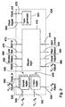
- the mixer 50 mixes the signal received by the antenna 10, filtered by the RF filter 20 and amplified by the low noise input amplifier LNA 40 during a reception process with a signal which it receives from a synthesizer circuit 120.
- the synthesizer circuit 120 is connected to the mixer 50 via a transmit (TX) filter 130, a transmit / receive (T / R) switch 140 and a phase shifter 150, which are connected in series.
- the synthesizer circuit 120, the transmission filter 130, the T / R switch 140, a preamplifier 160, a transmission filter 170, a power amplifier (PA) are a in the transmission / reception circuit of FIG Output matching filter 190, T / R switch 30, RF filter 20 and antenna 10 connected in series.
- the synthesizer circuit 120 comprises two inputs 200 and 210, ie a transmit (TX) data input 210 and a PLL-TX control bus input.
- the synthesizer circuit 120 further includes a compensation circuit 220, a transmit (TX) data filter 230, a phase lock circuit PLL 240 with a phase detector, a loop filter 250, a voltage controlled oscillator 260 and a frequency doubler 270.
- the transmit data filter 230 and the compensation circuit 220 is connected to the transmission data input 210 in order to receive the data to be transmitted via the same.
- the oscillator 260 is connected to the compensation circuit 220 via the loop filter 250 and the PLL 240.
- the oscillator 260 is via a feedback path also connected directly to the PLL 240 to form a phase locked loop with the loop filter 250 and the PLL.
- the PLL 240 is also connected at one of its inputs to the PLL-TX control bus input 200, via which it receives input control signals for the phase-locked loop.
- the oscillator 260 is also connected to the transmit data filter 230 to receive filtered transmit data therefrom.
- the output of the oscillator 260 is connected to the frequency Doppler 270, which in turn is connected to the transmission filter 130 and outputs the output signal of the synthesizer circuit 120.
- the transmit / receive circuit of FIG. 1 is supplied by a battery voltage V b . While some components of the transmit / receive circuit of FIG. 1 are powered directly by the battery voltage V b , some components are powered by separate voltage regulators.
- the low-noise input amplifier LNA 40, the power amplifier and the transmission output stage PA 180, the two intermediate frequency amplifiers IF-Amp1 + IF-Amp2 80 and 90, the voltage-controlled oscillator VCO 260 and the digital components of the synthesizer circuit 120 , ie the frequency doubler 270, the TX data filter 230, the compensation circuit 220 and the PLL 240 with the phase detector, are supplied by separate voltage regulators, which in turn are connected to the battery voltage V b .
- the bias voltage or the input bias of the LNA 40 and the PA 180 are further Voltage regulator 333 or 336 regulated.
- voltage regulators 280-310 and 330-336 are connected to battery voltage V b and each have an adjustment input.
- the adjust input of the voltage regulators 280-310 and 330-336 is used, as will be described in the following, to set the supply voltages or the bias voltage and thus the function of the corresponding electronic components in accordance with certain current operating parameters of the transmit / receive circuit.
- a selected filter 70 is connected in series in the reception path of the transmission / reception circuit.
- a selector circuit selects a suitable filter from a plurality of filters 70a and 70b in accordance with certain instantaneous operating parameters of the transmitting / receiving circuit.
- this selector circuit has an input Filter Select 340.
- the RSSI value ie the received signal strength
- LNA 40 the low-noise input amplifier
- VCO 260 the power amplifier 180 and the intermediate frequency amplifiers 80 and 90
- the LNA 40 can be regulated via its supply voltage or via the input bias (bias voltage). By reducing this voltage, the gain is reduced and the power loss is reduced.
- the control of the supply voltage is carried out via the voltage regulator 280 and the control of the bias voltage via the voltage regulator 333, both of which are dynamically adjustable DC-DC converters (DC-DC converters).
- the voltage regulator 280 is also used to place the LNA 40 in a standby mode. During standby mode, the LNA 40 is deactivated by interrupting its supply voltage. This avoids leakage currents that would normally arise during the actual standby operation of the LNA 40, ie if it were directly connected to the battery voltage V b .
- the voltage regulator 280 has its own standby operating state, in which it requires only a minimal supply current.
- the power amplifier 180, the intermediate frequency amplifiers 80 and 90 and the oscillator 260 are supplied by a voltage regulator 290, 300 and 310 with the lowest possible supply voltage, the power loss being reduced when the supply voltage is reduced and in a standby mode Leakage currents can be avoided.
- An advantage of using separate voltage regulators 280-310 and 330 for the individual components is that the individual components are thereby decoupled from one another. Supply voltage fluctuations, which would be caused by strong load changes, such as switching on or off one or more components, if all function blocks or electronic components without a controller directly with the same supply voltage would be avoided by this decoupling. Since these fluctuations also influence the actual receive and transmit signals, the signal-to-noise ratio is consequently improved.
- the VCO 260 oscillator can be controlled directly via its supply voltage. With a strong input signal, i.e. a high RSSI value, a higher phase noise of the oscillator 260 can be tolerated. Interferers or interference frequencies are mixed more strongly into the reception band, but this is harmless if the desired signal is sufficiently high.
- the power amplifier or the transmitting output stage can also be controlled by means of the RSSI value via its supply voltage, which is supplied by the voltage regulator 290, or via its bias voltage, which is supplied by the voltage regulator 336.
- the consideration of using the received signal strength to regulate the output gain is that it is assumed that a high RSSI value suggests a good radio connection to the opposite station or base station (not shown) and consequently the transmission power can be reduced ,
- a second RSSI measurement before the intermediate frequency filter 70 and a comparison with the actual RSSI value, which is measured after this filter 70, and a comparison of the two values can be used to infer the presence of interferers or interference frequencies.
- a broadband filter 70 can be selected from the plurality of filters 70a and 70b with a lower insertion loss via the control line Filter Select 340, as will be described below, thereby reducing the subsequent gain and power consumption can.
- the supply voltage of the digital components 320 of the Synthesizers 120 ie the frequency doubler 270, the transmit data filter 230, the compensation circuit 220 and the phase lock circuit 240, cannot be reduced directly, since the correct functioning of a digital circuit can no longer be guaranteed above a certain minimum voltage.
- the clock for the digital components is reduced if the performance is reduced or the capacity is reduced, since the switching delay caused by a reduction in the supply voltage can be tolerated due to the lower processing speed when the clock is reduced.
- the mixer supply could also be reduced when the input signal is high and the power consumption of the mixer reduced.
- the power management module 400 includes one Logic circuit 410, a clock generator 420, a plurality of switching regulators 430 and a plurality of linear regulators 440.
- the switching regulators 430 and linear regulators 440 correspond to the voltage regulators 280-310 and 330-336 shown in FIG. 1, it being noted that in the choice Which voltage regulator 280-310 and 330-336 is a switching regulator or a linear regulator, especially the efficiency and the output noise as well as the transient response must be considered.
- the voltage regulators 280 and 310 are preferably designed as linear regulators, since they have to take care of a low noise of the supply voltage. The same approach is used to select the other DC-DC converters.
- the control logic 410 of FIG. 2 has four inputs 450, 460, 470 and 475, in which the control logic 410 has four different instantaneous operating parameters, ie the received signal strength RSSI, received signal interference information (blocker detect), battery charge status information (low. Bat) and receives information about whether there is a transmission or a reception process, which are explained in more detail below.
- the control logic 410 Based on the current operating parameters received, the control logic 410 generates corresponding control signals which it outputs at a plurality of outputs 480, two outputs 490 and 500 and a plurality of outputs 510.
- the plurality of outputs 480 and 510 are connected to the plurality of voltage regulators 430 and 440 at their respective inputs 520 and 530, respectively.
- control logic 410 can control the supply voltages or the bias voltages of electronic components of the transmit / receive circuit are connected to outputs 540 and 550 of the plurality of voltage regulators 430 and 440, respectively, in such a way that the total power consumption of the transmitting / receiving circuit is reduced or minimized in accordance with the current operating parameters.
- the output 490 (clock adjust) is connected to an input 560 of the clock generator 420, which outputs an output 570 for the digital circuit components of the transmit / receive circuit (320 in FIG. 1).
- the plurality of switching regulators 430 also have an input Clock_in 580, via which they receive an internal clock for controlling the output voltage.
- the control logic 410 outputs a signal which, as will be explained in more detail below, depends on the input signals at the inputs 450-475 from the plurality of filters 70a and 70b (FIG. 1), a tolerable filter with less Select insertion loss.
- the operation of the control logic 410 will be described in more detail using a specific example, it is pointed out that, although only seven voltage regulators are shown in FIG. 1, the power management module 400 may include more or fewer voltage regulators that are suitable electronic components of the transmission / reception circuit are connected.
- 3 shows a dashed line voltage management module 600 that includes control logic 610 shown with a dashed line, a plurality of voltage regulators 620, 625, 630, 635, 640, 650, 660 and 670, and a clock generator 690.
- the control logic 610 comprises a plurality of control logic units 700, 710, 720, 730 and 740 and a correction circuit 750.
- the voltage management module comprises 600 of FIG. 3 four inputs Bat_IN, BLD_IN, RSSI_IN and RX / TX 760, 770, 780 and 785.
- the voltage management module 600 also includes ten outputs 790, 795, 800, 805, 810, 820, 830, 840, 850 and 860 ,
- control logic 610 The operation of the control logic 610 and the wiring of the voltage management module 600 and the connection of the outputs 790-860 to the respective electronic components of the transmission / reception circuit of FIG. 1 will now be described below.
- the LNA control logic unit 700 has an input connected to the RSSI_IN input of the voltage management module 600 in order to receive a value for the received signal strength.
- the LNA control logic unit 700 has an output connected to the LNA voltage regulator 620, which in turn is connected to the output LNA_OUT and outputs the supply voltage there to the low-noise input amplifier LNA 40 from FIG. 1.
- the LNA control logic unit 700 is connected at a further output to the voltage regulator 625, which in turn is connected to the output LNA_Bias and outputs the bias voltage to the low-noise input amplifier LNA 40 there.
- Control logic unit 700 is designed to, depending on the RSSI value received, output control signals to voltage regulators 620 and 625 such that they decrease the supply voltage and bias voltage for LNA 40 as the RSSI value increases. This takes into account that a high input signal strength requires less amplification. As a result, the gain is reduced and the power loss is reduced in order to save the power consumption by reducing the supply voltage and the bias voltage. In the present example, the supply voltage and the bias voltage are reduced in such a way that the lowest possible but sufficient amplification value results with low noise at the same time. However, it can be provided that either the supply voltage or the bias voltage of the LNA 40 is controlled and not both, in which case either the voltage regulator 625 (or 333 in FIG. 1) or the voltage regulator 620 (or 280 in FIG. 1) could be missing.
- the control logic unit 700 is also designed to put the LNA into a standby mode, e.g. if the transmission / reception circuit is in a transmission process.
- the LNA control logic unit 700 is connected to the input RX / TX 785, at which it receives a signal from a baseband processor (not shown) which indicates whether there is a transmission or reception process. If the LNA control logic unit 700 puts the LNA into a standby mode, the LNA control logic unit 700 outputs a corresponding control signal to the voltage regulator 620, which then generates 0 volts at its output and then is in its own standby or standby operating state is located, in which the standby mode requires only a minimal supply current.
- the LNA 40 (FIG. 1) is deactivated by interrupting the supply voltage.
- the advantage is that all leakage currents that would normally arise in the actual standby mode of the LNA 40 with an uninterrupted supply voltage are avoided.
- an MX control logic unit 710 is provided in the voltage management module 600 of FIG. 3, which is connected at one input to the RSSI_IN input 780 in order to receive the RSSI value, and at an output to the MXI Voltage regulator 630 is connected.
- the MX voltage regulator 630 is in turn connected to the intermediate frequency mixer 50 via the MX_OUT 800 output.
- the MX control logic unit 710 is designed to set the supply voltage of the mixer 50 according to the RSSI value via the MX voltage regulator 630.
- the MX control logic unit 710 reduces the mixer 50 supply voltage at a higher input signal strength value. For this purpose, the control logic 710 issues a corresponding control signal to the voltage regulator 630.
- the MX control logic unit provides a reduction in the gain and power consumption of the mixer 50 and thus a reduction in the total power consumption.
- the MX control logic 710 also performs the task of placing the mixer 50 in a standby mode when there is a transmit, as described above with reference to the LNA control logic unit.
- the control logic unit 710 like the LNA control logic unit 700, is connected to the input RX / TX in addition to the input RSSI_IN in order to receive information about the presence of a receiving or transmitting operation.
- the PA control logic unit 720 receives the RSSI value at an input from the input RSSI_IN 780 in order to output control signals to the PA voltage regulator 640 or the voltage regulator 635 at two outputs.
- the PA voltage regulator 640 is connected to the power amplifier PA 180 via the output PA_OUT 810 in order to supply the same with the supply voltage in accordance with the control signal from the PA control logic unit 720.
- the voltage regulator 635 is connected to the power amplifier PA 180 via the output PA_Bias 805 in order to supply the bias voltage to it according to the control signal from the PA control logic unit 720.
- the PA control logic unit 720 is designed to control the voltage regulators 635 and 640 via the control signals in such a way that the power amplifier 180 is supplied with a lower supply voltage and / or bias voltage when the RSSI value is higher.
- This mode of operation is based on the assumption that a high RSSI value indicates a good radio connection to the opposite station or base station (not shown), and consequently the amplification or the transmission power can be reduced.
- only the voltage regulator 635 (or 336 in FIG. 1) or the can also be used for the power management of the PA 180 Voltage regulator 640 (or 290 in FIG. 1) can be provided to regulate either the supply voltage or the bias voltage.
- the PA control logic unit 720 also takes on the task of putting the PA 180 into a standby mode when there is a receive operation.
- the control logic unit 720 is connected to the input RX / TX in addition to the input RSSI_IN in order to receive information about the presence of a reception or transmission process.
- the control logic unit 730 is connected to two inputs of the voltage management module 600, the BLD_IN and the RSSI_IN.
- Noise control logic unit 730 receives a second RSSI value via input BLD_IN, which is measured before intermediate frequency filter 70.
- a correction circuit 750 is connected between the noise control logic unit 730 and the input BLD_IN, which corrects the second RSSI value with the insertion loss of the currently selected filter 70.
- Noise control logic unit 730 has an output connected to VCO voltage regulator 650, which in turn is connected to oscillator VCO via output VCO_OUT 820.
- the noise control logic unit 730 outputs a control signal to the voltage regulator 650 such that the oscillator is supplied with a lower supply voltage by the voltage regulator 650 when the two RSSI values are essentially the same or a higher phase noise is tolerable, and is supplied with a higher supply voltage if the two RSSI values are further apart.
- the noise control logic unit 730 is also designed to further reduce the supply voltage to the VCO if the RSSI value increases because higher signal noise in the oscillator can generally be tolerated with a strong signal input strength. In this case, interferers are mixed more strongly into the reception band, but this is harmless if the desired signal is sufficiently high.
- the noise control logic unit 730 is also designed to output a control signal to the output 840 Filter_Out, which is connected to a selector circuit (not shown in Fig. 1) based on the comparison between the two RSSI values, such that a broadband filter is inserted into the filter Receive path of the transmit / receive circuit is switched if the RSSI values essentially match. Since a broadband filter has a lower insertion loss, this can also reduce power consumption.
- the output of the noise control logic unit 730 which is connected to the Filter_OUT output, is also connected to an input of the correction circuit 750.
- the noise control logic unit 730 is also connected at an output to the IF-Amp voltage regulator 660, which is connected via the output IF-Amp_OUT 830 to the two intermediate frequency amplifiers 80 and 90 (FIG. 1).
- the noise control logic unit 730 is designed to reduce the supply voltage of the intermediate frequency amplifiers 80 and 90 in the event that the RSSI values are essentially the same, since the intermediate frequency amplifiers 80 and 90 have a lower gain because of the broadband filter with lower insertion loss that is possible in this case is made possible. For this purpose, the noise control logic unit 730 in turn outputs a suitable control signal to the voltage regulator 660, and this in turn saves power loss. Like those described above Control logic units 700-720, control logic unit 730 is also connected to input RX / TX 785 in order to obtain information about whether a transmission or reception process is currently taking place, for example the supply voltage of IF-Amp voltage regulator 660 being switched off when a transmission process is present can.
- the control logic unit 740 is connected to the RSSI_IN and RX / TX inputs, and is designed to determine the supply voltage and the clock for the digital components 320, ie the PLL 240, based on the RSSI value and the information from the baseband processor Frequency Doppler 270, the compensation circuit 220 and the TX data filter 230 to set.
- the digital part control logic unit 740 is connected to the voltage regulator 670 at a first output and to the clock generator 690 at a second output.
- the digital part control logic unit 740 sends a corresponding control signal clock generator 690, which indicates that the digital components can be supplied with a reduced clock.
- the clock generator 690 outputs a clock with a lower speed for the digital components at the output CL_dig 850 in accordance with the control signal from the digital part control logic unit 740.
- the supply voltage can also be reduced, since the switching delay caused thereby can be tolerated due to the lower processing speed.
- control logic unit 740 is designed to send a control signal to the voltage regulator 670 in such a case that the digital part 320 (FIG. 1) of the synthesizer circuit 120 is supplied with a lower supply voltage by the voltage regulator 670 via the output Dig_OUT 860, which in turn Power loss is saved.
- the control logic unit 740 is also designed to switch off the supply voltage of any possible individual components depending on the information received from the baseband processor as to whether there is currently a transmission or reception process or neither.
- the BAT_IN 760 input is connected to each control logic unit 700-740 to provide battery charge status information to each control logic unit 700-740.
- the control logic units 700-740 are designed to use this information about the state of charge of the battery (not shown) in addition to the information mentioned above, for example to effect an especially low-loss operating mode while sacrificing the quality of the received data (RX data), to be able to carry out the most important functions of the transmit / receive circuit even when the battery is almost empty.
- FIG. 3 shows a power management module which consists of control logic, a plurality of digitally adjustable linear and switching regulators and a variable clock generator.
- the control logic reads in signals that characterize the requirements for the overall system. In the present case, these are the RSSI signals (RSSI, blocker detected), signals from the baseband processor of the transmission / reception circuit or signals from the battery management system, such as a charge status display or an indication that the charge capacity has fallen below a certain threshold value.
- the logic must process these signals and generate control signals which are then passed on to the adjustable voltage regulators and thus control the output voltages of the same. As a result, the supply voltage is adjusted, and thus indirectly the control of the function of the individual blocks.
- signals for setting the clock frequency, for selecting the filters and for regulating the gains are generated in accordance with the measured input signals of the control logic. In this way, a low-performance, optimized operation of the individual system blocks or electronic components as well as the entire system can be guaranteed.
- control logic can, for example, have further inputs through which it receives further signals from the baseband processor.
- number of outputs can vary, with further or fewer parameters being able to be controlled in accordance with the current operating parameters.
- the present invention is directed to transmit / receive circuits for cordless telephones, data transmission devices such as e.g. Data transmission devices of the DECT and Bluetooth standards, mobile phones, such as GSM, DCS, PCS mobile phones, and ISM band data transmissions applicable.
- control logic units of Fig. 3 are designed by the circuit design to perform the operation described above or that they each additionally have a look-up table in which responses to certain input signals to the control logic units are stored. It is also noted that the control logic may be formed using a single look-up table in which a set of values for each voltage regulator, clock generator and filter selector circuit for each set of input values are stored at the inputs of the control logic and power management module, respectively is.
- control logic units are constructed in analog or digital form.
- control logic units are constructed digitally, digital control signals being output by the control logic units.
- transceiver part of Fig. 1 is not essential to the present invention.
- individual components can be designed differently, e.g. the voltage regulator.
Abstract
Description
Die vorliegende Erfindung bezieht sich auf Sende/Empfangsschaltungen und insbesondere auf Sende/Empfangsschaltungen für schnurlose Telephone, Datenübertragungsgeräte, wie z.B. Datenübertragungsgeräte des DECT- und Bluetooth-Standards, Mobiltelephone, wie z.B. GSM-, DCS-, PCS-Mobiltelephone, und ISM-Band-Datenübertragungen.The present invention relates to transmission / reception circuits and in particular to transmission / reception circuits for cordless telephones, data transmission devices such as e.g. Data transmission devices of the DECT and Bluetooth standards, mobile phones, such as GSM, DCS, PCS mobile phones, and ISM band data transfers.
Für Sende/Empfangs-Schaltungen, die bei schnurlosen bzw. tragbaren Sende/Empfangs-Einheiten verwendet werden, ist es aufgrund der begrenzten zur Verfügung stehenden Batteriekapazität besonders wichtig, daß dieselben einen niedrigen Leistungsverbrauch aufweisen. Bei den zur Zeit verwendeten Sende/Empfangsschaltungen für die im vorhergehenden erwähnten Geräte wird der Leistungsverbrauch während des Betriebs der Sende/Empfangs-Schaltung verringert, indem durch eine Leistungsverwaltung ganze Systeme, die mehrere Blöcke, wie z.B. Sende- oder Empfangs-Pfad, enthalten, ein- oder ausgeschaltet bzw. in einen Standby-Betrieb versetzt werden. Während des Sendens können beispielsweise ein Mischer, ein Zwischenfrequenzverstärker und eine Frequenzmodulationserfassungsschaltung bzw. ein FM-Detektor, soweit dieselben vorhanden sind, deaktiviert werden. Während eines Empfangsvorgangs können beispielsweise eine Sendeendstufe und ein Vorverstärker ausgeschaltet werden. Der Synthesizer bzw. die Frequenzerzeugungsschaltung ist sowohl während des Sendeals auch des Empfangsvorgangs erforderlich und kann folglich nur dann in einen Standby- (Bereitschafts-) Betriebszustand versetzt werden, wenn weder gesendet noch empfangen wird.For transmission / reception circuits which are used in cordless or portable transmission / reception units, it is particularly important because of the limited available battery capacity that they have a low power consumption. In the transmission / reception circuits currently used for the devices mentioned above, the power consumption during operation of the transmission / reception circuit is reduced by using entire systems, which comprise several blocks, e.g. Send or receive path, included, switched on or off or put into a standby mode. For example, a mixer, an intermediate frequency amplifier and a frequency modulation detection circuit or an FM detector, if present, can be deactivated during transmission. For example, a transmission output stage and a preamplifier can be switched off during a reception process. The synthesizer or the frequency generation circuit is required both during the transmission and the reception process and can consequently only be put into a standby (standby) operating state if neither transmission nor reception is carried out.
Neben diesem Ein- und Ausschalten von einzelnen Komponenten existiert bei einigen derzeit verfügbaren Sende/Empfangsschaltungen eine kontinuierliche, dynamische Steuerung der Verstärkung des Zwischenfrequenzverstärkers sowie der Sendeendstufe, die während des Betriebs dynamisch geregelt werden. Zur Steuerung des Zwischenfrequenzverstärkers wird die Empfangssignalstärke RSSI (RSSI = Receive Signal Strength Indicator) gemessen und die Verstärkung entsprechend dieser Empfangssignalstärke bzw. dem empfangenen Signalpegel eingestellt, was als AGC- (Automatic Gain Control = automatische Verstärkungssteuerung) Steuerung bezeichnet wird.In addition to this switching individual components on and off, some currently available transmission / reception circuits have a continuous, dynamic control of the amplification of the intermediate frequency amplifier and of the transmission output stage, which are dynamically regulated during operation. To control the intermediate frequency amplifier, the received signal strength RSSI (RSSI = Receive Signal Strength Indicator) is measured and the gain is set in accordance with this received signal strength or the received signal level, which is referred to as AGC (Automatic Gain Control) control.
Ein Nachteil der bestehenden Sende/Empfangs-Systeme besteht darin, daß viele Funktionsblöcke während des Betriebs für die eigentlichen Aufgaben überdimensioniert sind und folglich zu viel Verlustleistung erfordern. Der Grund hierfür besteht darin, daß die einzelnen Komponenten für die schlechtesten Empfangs- und Sendebedingungen ausgelegt sein müssen, d.h. für den "Worst-Case"-Fall mit maximalen Nachbarkanalstörern und minimaler Empfangsleistung. Bei DECT-Systemen kann die Empfangssignalstärke jedoch beispielsweise zwischen -94 dBm und +10 dBm variieren, wobei der Empfangsleistungsminimalwert von -94 dBm nur in den seltensten Fällen erreicht wird. Auch die Nachbarkanalstörer erreichen nur selten die in den Spezifikationen angegebenen Maximalwerte, falls sie überhaupt vorhanden sind.A disadvantage of the existing transmit / receive systems is that many function blocks are oversized for the actual tasks during operation and consequently require too much power loss. The reason for this is that the individual components must be designed for the worst reception and transmission conditions, i.e. for the "worst case" case with maximum adjacent channel interference and minimal reception power. In DECT systems, however, the received signal strength can vary, for example, between -94 dBm and +10 dBm, with the received power minimum value of -94 dBm being reached only in the rarest of cases. The adjacent channel interferers rarely reach the maximum values specified in the specifications, if they exist at all.
Folglich sind viele Komponenten von Sende/Empfangsschaltungen durchschnittlich, d.h. den größten Teil der Betriebszeit über, überdimensioniert, was zu einem unnötig hohen Leistungsverbrauch der Schaltung führt. Viel zu hohe Anforderungen werden an das Phasenrauschen des Oszillators (VCO; VCO = Voltage Controlled Oscillator) einer Sende/Empfangs-Schaltung gestellt, die lediglich dann notwendig sind, wenn das Empfangssignal sehr schlecht ist, oder Störsignale starker Leistung empfangen werden. Die rauscharmen Eingangsverstärker und das Zwischenfrequenzfilter sind ebenfalls für widrigste Empfangsbedingungen ausgelegt und somit für die meiste Zeit des Betriebs überdimensioniert.As a result, many components of transmit / receive circuits are average, i.e. over the largest part of the operating time, oversized, which leads to an unnecessarily high power consumption of the circuit. Much too high demands are placed on the phase noise of the oscillator (VCO = VCO = Voltage Controlled Oscillator) of a transmit / receive circuit, which are only necessary if the received signal is very bad or interference signals of high power are received. The low-noise input amplifiers and the intermediate frequency filter are also designed for the most adverse reception conditions and are therefore oversized for most of the time.
Die Aufgabe der vorliegenden Erfindung. besteht darin, eine Sende/Empfangsschaltung zu schaffen, bei der der Betriebsleistungsverbrauch niedriger ist.The object of the present invention. is one To create transmit / receive circuit in which the operating power consumption is lower.
Diese Aufgabe wird durch eine Sende/Empfangsschaltung gemäß Anspruch 1 gelöst.This object is achieved by a transmission / reception circuit according to
Eine erfindungsgemäße Sende/Empfangsschaltung weist eine Mehrzahl von elektronischen Komponenten auf, die verbunden sind, um zum Senden und Empfangen von Daten zusammenzuwirken, wobei die Komponenten durch Steuersignale steuerbar sind. Die Sende/Empfangsschaltung weist ferner eine Steuerlogik, die mit der Mehrzahl von elektronischen Komponenten verbunden ist, zum Überwachen von momentanen Betriebsparametern der Sende/Empfangsschaltung und zum Ausgeben von Steuersignalen an die Mehrzahl von elektronischen Komponenten abhängig von den momentanen Betriebsparametern auf, wobei die Steuersignale bei den Komponenten zumindest zwei Parameter aus einer Gruppe von Parametern umfassen, die aus der Versorgungsspannung, der Verstärkung, einer Filterauswahl und einer Taktgeschwindigkeit, mit der wenigstens eine der Komponenten betrieben wird, besteht.A transmission / reception circuit according to the invention has a plurality of electronic components which are connected in order to cooperate for the transmission and reception of data, the components being controllable by control signals. The transmit / receive circuit also has control logic, which is connected to the plurality of electronic components, for monitoring current operating parameters of the transmit / receive circuit and for outputting control signals to the plurality of electronic components depending on the current operating parameters, the control signals being at the components comprise at least two parameters from a group of parameters consisting of the supply voltage, the amplification, a filter selection and a clock speed with which at least one of the components is operated.
Gemäß einem Ausführungsbeispiel der vorliegenden Erfindung umfaßt eine Sende/Empfangsschaltung einen Sendeteil, einen Empfangsteil und eine Synthesizer-Schaltung bzw. Frequenzerzeugungsschaltung. Die Steuerlogik steuert über Spannungssignale abhängig von der Empfangssignalstärke oder ähnlichen Signalen, wie z.B. Batterieladezustandsinformationen, Empfangssignalstörinformationen und Signale eines Basisband-Prozessors, eine Mehrzahl von Spannungsreglern die mit entsprechenden elektronischen Komponenten der Sende/Empfangsschaltung verbunden sind. Die Sende/Empfangsschaltung umfaßt ferner mehrere Zwischenfrequenzfilter, aus denen die Steuerlogik einen den momentanen Betriebsparametern angepaßtes Filter auswählen kann, das einerseits eine ausreichend schmale Frequenzbandbreite und andererseits einen möglichst niedrigen Einfügeverlust aufweist. Die Signal/Empfangsschaltung verwendet als momentane Betriebsparameter die Empfangssignalstärke, Batterieladezustandsinformationen, Empfangssignalstörinformationen und Signale eines Basisband-Prozessors, die angeben, ob ein Sende- oder Empfangsvorgang vorliegt, um die elektronischen Komponenten derart zu steuern, daß die Versorgungsspannung und die Verstärkung ansprechend auf eine Zunahme der Eingangssignalstärke reduziert, die Versorgungsspannung und die Verstärkung ansprechend auf eine Abnahme des Batterieladezustands weiter reduziert, bei Abnahme von Empfangssignalstörungen ein Filter mit niedrigerer Einfügedämpfung und breiterem Durchlaßfrequenzband ausgewählt, und die Taktgeschwindigkeit ansprechend auf eine Abnahme der Datenratenübertragungsrate reduziert wird. Zur Steuerung der Verstärkung und der Versorgungsspannung werden Spannungsregler, wie z.B. Linear- und Schaltregler, verwendet.According to an exemplary embodiment of the present invention, a transmission / reception circuit comprises a transmission part, a reception part and a synthesizer circuit or frequency generation circuit. The control logic controls a plurality of voltage regulators via voltage signals depending on the received signal strength or similar signals, such as, for example, battery charge status information, received signal interference information and signals from a baseband processor, which are connected to corresponding electronic components of the transmit / receive circuit. The transmit / receive circuit further comprises a plurality of intermediate frequency filters, from which the control logic can select a filter which is adapted to the current operating parameters and which, on the one hand, has a sufficiently narrow frequency bandwidth and, on the other hand, the lowest possible insertion loss. The signal / receive circuit uses the received signal strength as the current operating parameters, Battery level information, receive signal interference information, and signals from a baseband processor, indicating whether there is a transmit or receive operation to control the electronic components such that the supply voltage and gain reduce in response to an increase in input signal strength, the supply voltage and gain in response a decrease in the battery state of charge is further reduced, a filter with a lower insertion loss and a wider pass frequency band is selected when reception signal interference decreases, and the clock speed is reduced in response to a decrease in the data rate transmission rate. Voltage regulators such as linear and switching regulators are used to control the amplification and the supply voltage.
Ein Vorteil der vorliegenden Erfindung besteht darin, daß durch Verwenden der momentanen Betriebsparameter, wie z.B. den Empfangsbedingungen oder dem Batterieladezustand, ein angepaßter Betriebszustand der Sende/Empfangsschaltung sichergestellt werden kann. Anders als bei herkömmlichen Sende/Empfangsschaltungen, die einzelne Teilsysteme, wie z.B. den Sende- oder Empfangspfad, aktivieren oder deaktivieren, oder lediglich den Zwischenfrequenzverstärker oder die Sendeendstufe dynamisch regeln, wird bei der vorliegenden Erfindung durch das dynamische Steuern, Konfigurieren und Versorgen von einzelnen Komponenten entsprechend den momentanen Betriebsparametern während des Betriebes ein höchst effizienter, leistungsoptimierter Betrieb der gesamten Sende/Empfangsschaltung erzielt.An advantage of the present invention is that by using the current operating parameters, e.g. the reception conditions or the battery charge state, an adapted operating state of the transmission / reception circuit can be ensured. In contrast to conventional transmit / receive circuits, the individual subsystems, e.g. activate or deactivate the transmission or reception path, or only dynamically regulate the intermediate frequency amplifier or the transmission output stage, in the present invention, through the dynamic control, configuration and supply of individual components in accordance with the current operating parameters during operation, a highly efficient, performance-optimized operation of the total transmission / reception circuit achieved.
Zudem wird durch die getrennte Leistungsversorgung der einzelnen elektronischen Komponenten der Schaltung durch die verschiedenen Spannungsregler eine Entkopplung aller Komponenten erzielt. Durch diese Entkopplung wirken sich starke Laständerungen, wie z.B. das Ein- oder Ausschalten einer oder mehrerer Komponenten, nicht als eine Schwankung der Versorgungsspannung aus, wie es der Fall ist, wenn die elektronischen Komponenten direkt mit der gleichen Spannungsversorgung verbunden wären. Zudem können die Spannungsregler verwendet werden, um die elektronischen Komponenten in einen Standby-Modus zu versetzen, bei dem den elektronischen Komponenten keine Versorgungsspannung zugeführt wird, und folglich Leckströme vermieden werden, und die Spannungsregler selbst einen minimalen Versorgungsstrom erfordern. Auf diese Weise kann folglich die Betriebszeit einer batteriebetriebenen Sende/Empfängereinheit verlängert werden.In addition, the separate power supply of the individual electronic components of the circuit by means of the various voltage regulators ensures that all components are decoupled. As a result of this decoupling, strong changes in load, such as the switching on or off of one or more components, do not have the effect of a fluctuation in the supply voltage, as is the case when the electronic Components would be connected directly to the same power supply. In addition, the voltage regulators can be used to place the electronic components in a standby mode, in which no supply voltage is supplied to the electronic components, and consequently leakage currents are avoided, and the voltage regulators themselves require a minimal supply current. In this way, the operating time of a battery-operated transceiver unit can be extended.
Folglich kann durch Verwenden der erfindungsgemäßen Sende/Empfangsschaltung, die die einzelnen elektronischen Komponenten intelligent, dynamisch versorgt, steuert und konfiguriert, (a) die Betriebszeit einer batteriebetriebenen Sende/Empfangseinheit verlängert, (b) bei gleichbleibender Betriebszeit die maximale Kapazität der Batterie und somit deren Volumen bzw. deren Gewicht verringert, und (c) die in der Sende/Empfangseinheit verbrauchte Verlustleistung reduziert und somit wiederum die aufwendigen Kühlkörper verkleinert werden, wodurch das gesamte Volumen eines die Sende/Empfangsschaltung enthaltenden Gerätes verringert werden kann.Consequently, by using the transmission / reception circuit according to the invention, which intelligently, dynamically supplies, controls and configures the individual electronic components, (a) the operating time of a battery-operated transmitting / receiving unit can be extended, (b) the operating capacity of the battery and thus its maximum capacity Volume or their weight is reduced, and (c) the power loss consumed in the transmitter / receiver unit is reduced, and in turn the expensive heat sink is reduced, as a result of which the total volume of a device containing the transmitter / receiver circuit can be reduced.
Bevorzugte Ausführungsbeispiele der vorliegenden Erfindung werden nachfolgend bezugnehmend auf die beiliegenden Zeichnungen näher erläutert. Es zeigen:
- Fig. 1
- ein Blockdiagramm eines Sende/Empfangsteils einer Sende/Empfangsschaltung gemäß einem Ausführungsbeispiel der vorliegenden Erfindung;
- Fig. 2
- ein Blockdiagramm eines Leistungsverwaltungsmoduls zur Verwendung bei der Sende/Empfangsschaltung von Fig. 1; und
- Fig. 3
- ein detaillierteres Blockdiagramm eines Leistungsverwaltungsmoduls.
- Fig. 1
- a block diagram of a transmission / reception part of a transmission / reception circuit according to an embodiment of the present invention;
- Fig. 2
- 1 is a block diagram of a power management module for use with the transmit / receive circuit of FIG. 1; and
- Fig. 3
- a more detailed block diagram of a performance management module.
Wie es im folgenden beschrieben werden wird, wird eine erfindungsgemäße Sende/Empfangsschaltung entsprechend momentanen Betriebsparametern, wie z.B. Umgebungsbedingungen bzw. Empfangsbedingungen, oder entsprechend den sich daraus ergebenden Anforderungen intelligent versorgt, gesteuert und konfiguriert. Durch Ermittlung der Anforderungen an die Sende/Empfangsschaltung, wie z.B. einer hohen Anforderung an die Verstärkung und Rauschunterdrückung bei niedriger Eingangssignalstärke, wird immer ein minimaler Leistungsverbrauch gewährleistet. Gemäß den bezugnehmend auf Fig. 1-3 beschriebenen Ausführungsbeispielen wird diese Versorgung, Steuerung und Konfigurierung durch ein Leistungsverwaltungsmodul durchgeführt, das aus einer Steuerlogik, mehreren digital einstellbaren Linear- und Schaltreglern und einem variablen Taktgenerator besteht. Die Steuerlogik liest Signale, die die Anforderungen an das Gesamtsystem charakterisieren, bzw. die momentanen Betriebsparameter ein. Dies können beispielsweise RSSI-Signale, Signale vom Basisband-Prozessor der Sende/Empfangsschaltung oder Signale von einem Batterieverwaltungssystem sein, wie z.B. eine Ladezustandsanzeige. Entsprechend dieser Signale werden dann Steuerungssignale erzeugt und ausgegeben, die einen leistungsarmen, optimierten Betrieb der einzelnen Systemblöcke bzw. der einzelnen elektronischen Komponenten sowie des gesamten Systems sicherstellen. Diese Steuerungssignale regeln die Ausgangsspannungen der einstellbaren Linear- und Schaltregler und steuern somit die Versorgung und indirekt die Funktion der einzelnen Blöcke.As will be described in the following, a transmission / reception circuit according to the invention is designed according to current operating parameters, e.g. Ambient conditions or reception conditions, or intelligently supplied, controlled and configured according to the resulting requirements. By determining the requirements for the transmission / reception circuit, such as A high requirement for the amplification and noise suppression with low input signal strength, a minimal power consumption is always guaranteed. According to the exemplary embodiments described with reference to FIGS. 1-3, this supply, control and configuration is carried out by a power management module which consists of control logic, a plurality of digitally adjustable linear and switching regulators and a variable clock generator. The control logic reads in signals that characterize the requirements for the overall system or the current operating parameters. These can be, for example, RSSI signals, signals from the baseband processor of the transmitting / receiving circuit or signals from a battery management system, such as a charge level indicator. Control signals are then generated and output in accordance with these signals, which ensure low-power, optimized operation of the individual system blocks or of the individual electronic components and of the entire system. These control signals regulate the output voltages of the adjustable linear and switching regulators and thus control the supply and indirectly the function of the individual blocks.
Bezugnehmend auf Fig. 1 wird nun der Sendeteil, der Empfangsteil und die Synthesizer-Schaltung einer Sende/Empfangsschaltung gemäß einem Ausführungsbeispiel der vorliegenden Erfindung beschrieben.1, the transmission part, the reception part and the synthesizer circuit of a transmission / reception circuit according to an embodiment of the present invention will now be described.
Entlang einer Empfangsrichtung sind bei der Sende/Empfangsschaltung von Fig. 1 eine Antenne 10, ein Hochfrequenzfilter (HF-Filter) 20, ein Sende/Empfangsschalter (T/R-Schalter) 30, ein rauscharmer Eingangsverstärker 40 - (LNA; LNA = Low-Noise Amplifier), ein Zwischenfrequenzmischer 50 (IR-Mischer), ein Phasenschieber 60, ein ausgewähltes Zwischenfrequenzfilter 70, wie z.B. ein Zwischenfrequenzoberflächenwellen- (SAW-) Filter, zwei Zwischenfrequenzverstärker 80 und 90 (IF-Amp1 und IF-Amp2), eine Frequenzmodulationserfassungsschaltung bzw. ein FM-Detektor 100 und ein Empfangs-(RX-) Filter 110 in Reihe geschaltet.1, an
Der Mischer 50 mischt das durch die Antenne 10 empfangene, durch das HF-Filter 20 gefilterte und durch den rauscharmen Eingangsverstärker LNA 40 verstärkte Signal während eines Empfangsvorgangs mit einem Signal, das derselbe von einer Synthesizer-Schaltung 120 empfängt. Die Synthesizerschaltung 120 ist mit dem Mischer 50 über ein Sende- (TX-) Filter 130, einen Sende/Empfangs- (T/R-) Schalter 140 und einen Phasenschieber 150, die in Reihe geschaltet sind, verbunden.The
Entlang einer umgekehrten Richtung, d.h. einer Senderichtung, sind bei der Sende/Empfangsschaltung von Fig. 1 die Synthesizerschaltung 120, das Sendefilter 130, der T/R-Schalter 140, ein Vorverstärker 160, ein Sendefilter 170, ein Leistungsverstärker (PA; PA = Power Amplifier) 180, ein Ausgangsanpassungsfilter 190, der T/R-Schalter 30, das HF-Filter 20 und die Antenne 10 in Reihe geschaltet.Along a reverse direction, i.e. 1, the
Die Synthesizerschaltung 120 umfaßt zwei Eingänge 200 und 210, d.h. einen Sende (TX-) Dateneingang 210 und einen PLL-TX-Steuerungsbuseingang. Die Synthesizerschaltung 120 umfaßt ferner eine Kompensationsschaltung 220, ein Sende-(TX-) Datenfilter 230, eine Phasenverriegelungsschaltung PLL 240 mit einem Phasendetektor, ein Schleifen- bzw. Loop-Filter 250, einen spannungsgesteuerten Oszillator 260 und einen Frequenzdoppler 270. Das Sendedatenfilter 230 und die Kompensationsschaltung 220 sind mit dem Sendedateneingang 210 verbunden, um über denselben die zu sendenden Daten zu empfangen. Der Oszillator 260 ist über das Schleifenfilter 250 und die PLL 240 mit der Kompensationsschaltung 220 verbunden. Der Oszillator 260 ist über einen Rückkopplungsweg ferner direkt mit der PLL 240 verbunden, um mit dem Loop-Filter 250 und der PLL einen Phasenregelkreis zu bilden. Die PLL 240 ist an einem ihrer Eingänge ferner mit dem PLL-TX-Steuerungsbuseingang 200 verbunden, über den dieselbe Eingangssteuersignale für den Phasenregelkreis erhält. Der Oszillator 260 ist ferner mit dem Sendedatenfilter 230 verbunden, um von demselben gefilterte Sendedaten zu empfangen. Der Ausgang des Oszillators 260 ist mit dem Frequenzdoppler 270 verbunden, der wiederum mit dem Sendefilter 130 verbunden ist und das Ausgangssignal der Synthesizerschaltung 120 ausgibt.The
Die Sende/Empfangsschaltung von Fig. 1 wird von einer Batteriespannung Vb versorgt. Während einige Komponenten der Sende/Empfangsschaltung von Fig. 1 direkt durch die Batteriespannung Vb versorgt werden, werden einige Komponenten durch getrennte Spannungsregler versorgt. In dem vorliegenden Beispiel von Fig. 1 werden der rauscharme Eingangsverstärker LNA 40, der Leistungsverstärker bzw. die Sendeendstufe PA 180, die beiden Zwischenfrequenzverstärker IF-Amp1 + IF-Amp2 80 und 90, der spannungsgesteuerte Oszillator VCO 260 und die digitalen Komponenten der Synthesizerschaltung 120, d.h. der Frequenzdoppler 270, das TX-Datenfilter 230, die Kompensationsschaltung 220 und die PLL 240 mit dem Phasendetektor, durch getrennte Spannungsregler versorgt, die ihrerseits wiederum mit der Batteriespannung Vb verbunden sind. Insbesondere werden die Versorgungsspannung des rauscharmen Eingangsverstärkers LNA 40 von einem Spannungsregler 280, die Versorgungsspannung des Leistungsverstärkers 180 von einem Spannungsregler 290, die Versorgungsspannung der Zwischenfrequenzverstärker 80 und 90 von einem Spannungsregler 300, die Versorgungsspannung des Oszillators 260 von einem Spannungsregler 310 und die Versorgungsspannung der digitalen Komponenten 320 (d.h. innerhalb des Rahmens mit Strichlinie angezeigt) der digitalen Schaltung 120 von einem Spannungsregler 330 versorgt. Zusätzlich werden bei der in Fig. 1 gezeigten Schaltung die Biasspannung bzw. die Eingangsvorspannung des LNA 40 und des PA 180 über weitere Spannungsregler 333 bzw. 336 geregelt. Wie es zu sehen ist, sind die Spannungsregler 280-310 und 330-336 mit der Batteriespannung Vb verbunden und weisen jeweils einen Einstellungseingang (Adjust) auf. Der Adjust-Eingang der Spannungsregler 280-310 und 330-336 wird, wie es im folgenden beschrieben werden wird, verwendet, um die Versorgungsspannungen bzw. die Biasspannung und somit die Funktion der entsprechenden elektronischen Komponenten entsprechend bestimmten momentanen Betriebsparametern der Sende/Empfangsschaltung einzustellen.1 is supplied by a battery voltage V b . While some components of the transmit / receive circuit of FIG. 1 are powered directly by the battery voltage V b , some components are powered by separate voltage regulators. In the present example from FIG. 1, the low-noise
Wie es bereits im vorhergehenden erwähnt wurde, ist ein ausgewähltes Filter 70 seriell in den Empfangsweg der Sende/Empfangsschaltung geschaltet. Hierzu ist es vorgesehen, daß eine Auswählerschaltung (nicht gezeigt) entsprechend bestimmten momentanen Betriebsparametern der Sende/Empfangsschaltung ein geeignetes Filter aus einer Mehrzahl von Filtern 70a und 70b auswählt. Diese Auswählerschaltung weist hierzu einen Eingang Filter Select 340 auf.As already mentioned above, a selected
Anhand von Fig. 1 wird im folgenden beschrieben auf welche Art und Weise der Sende/Empfangsteil der Sende/Empfangsschaltung von Fig. 1 in Hinblick auf den Leistungsverbrauch gesteuert werden kann. Die Funktionsweise der Sende/Empfangsschaltung in Hinblick auf ihre Funktion als Sender und Empfänger geht für einen Fachmann auf diesem Gebiet aus dem Blockdiagramm von Fig. 1 und der vorhergehenden Beschreibung hervor und wird deshalb im weiteren nicht näher beschrieben.The manner in which the transmission / reception part of the transmission / reception circuit of FIG. 1 can be controlled with regard to the power consumption is described below with reference to FIG. 1. The mode of operation of the transmission / reception circuit with regard to its function as a transmitter and receiver is apparent to a person skilled in the art from the block diagram of FIG. 1 and the preceding description and is therefore not described in more detail below.
Um die Sende/Empfangsschaltung von Fig. 1 immer mit der minimal notwendigen Verlustleistung zu betreiben, müssen möglichst viele Informationen über die an dieselbe gestellten Anforderung zur Verfügung stehen. Die bei dem vorliegenden Ausführungsbeispiel wichtigste Information stellt der RSSI-Wert, d.h. die Empfangssignalstärke, dar, die in dem vorliegenden Fall bei den Zwischenfrequenzverstärkern 80 und 90 abgelesen wird, wie es bei 350 dargestellt ist, und mit dessen Hilfe der rauscharme Eingangsverstärker LNA 40, der Oszillator VCO 260, der Leistungsverstärker 180 und die Zwischenfrequenzverstärker 80 und 90 gesteuert werden können, wie es im folgenden beschrieben werden wird.In order to always operate the transmit / receive circuit of FIG. 1 with the minimum necessary power dissipation, as much information as possible must be available about the request placed on it. The most important information in the present exemplary embodiment is the RSSI value, ie the received signal strength, which is read in the present case from the
Der LNA 40 kann in den meisten Fällen über seine Versorgungsspannung oder über die Eingangsvorspannung (Biasspannung) geregelt werden. So wird durch Reduzierung dieser Spannung die Verstärkung reduziert und die Verlustleistung verringert. Die Steuerung der Versorgungsspannung wird über den Spannungsregler 280 und die Steuerung der Biasspannung über den Spannungsregler 333 durchgeführt, die beide dynamisch einstellbare DC-DC-Wandler (Gleichspannungs-Gleichspannungs-Wandler) sind. Der Spannungsregler 280 wird ferner verwendet, um den LNA 40 in einen Standby-Modus bzw. einen Bereitschaftsmodus zu versetzen. Während des Standby-Modus wird der LNA 40 durch Unterbrechung der Versorgungsspannung desselben deaktiviert. Hierdurch werden Leckströme, die normalerweise bei dem eigentlichen Standby-Betrieb des LNA 40 entstehen würden, d.h. wenn derselbe direkt mit der Batteriespannung Vb verbunden wäre, vermieden. Zudem weist der Spannungsregler 280 einen eigenen Standby-Betriebszustand auf, bei dem derselbe nur einen minimalen Versorgungsstrom erfordert.In most cases, the
Ebenso wie der LNA 40 werden auch der Leistungsverstärker 180, die Zwischenfrequenzverstärker 80 und 90 und der Oszillator 260 von einem Spannungsregler 290, 300 bzw. 310 mit einer möglichst niedrigen Versorgungsspannung versorgt, wobei bei Reduzierung der Versorgungsspannung die Verlustleistung verringert und bei einem Standby-Modus Leckströme vermieden werden. Ein Vorteil der Verwendung von getrennten Spannungsreglern 280-310 und 330 für die einzelnen Komponenten besteht darin, daß die einzelnen Komponenten hierdurch voneinander entkoppelt sind. Versorgungsspannungsschwankungen, die durch starke Laständerungen, wie beispielsweise das Ein- oder Ausschalten einer oder mehrerer Komponenten, hervorgerufen werden würden, wenn alle Funktionsblöcke bzw. elektronischen Komponenten ohne Regler direkt mit der gleichen Versorgungsspannung verbunden wären, werden durch diese Entkopplung vermieden. Da diese Schwankungen auch die eigentlichen Empfangs- und Sendesignale beeinflussen, wird folglich das Signalrauschleistungsverhältnis verbessert.Like the
Der Oszillator VCO 260 kann, wie der LNA 40 auch, direkt über seine Versorgungsspannung gesteuert werden. Bei einem starken Eingangssignal, d.h. einem hohen RSSI-Wert, des Empfängerteils kann ein höheres Phasenrauschen des Oszillators 260 toleriert werden. Störer bzw. Störfrequenzen werden hierbei zwar stärker in das Empfangsband gemischt, jedoch ist dies bei ausreichend hohem Pegel des gewünschten Signals unbedenklich.Like the
Auch der Leistungsverstärker bzw. die Sendeendstufe kann mittels des RSSI-Werts über seine Versorgungsspannung, die durch den Spannungsregler 290 geliefert wird, oder über seine Biasspannung, die durch den Spannungsregler 336 geliefert wird, gesteuert werden. Die Überlegung, die Empfangssignalstärke zu verwenden, um die Ausgangsverstärkung zu regeln, besteht darin, daß angenommen wird, daß ein hoher RSSI-Wert auf eine gute Funkverbindung zur Gegenstation bzw. Basisstation (nicht gezeigt) schließen läßt, und folglich die Sendeleistung reduziert werden kann.The power amplifier or the transmitting output stage can also be controlled by means of the RSSI value via its supply voltage, which is supplied by the
Durch eine zweite RSSI-Messung vor dem Zwischenfrequenzfilter 70 und einen Vergleich mit dem eigentlichen RSSI-Wert, der nach diesem Filter 70 gemessen wird, und einen Vergleich der beiden Werte kann auf das Vorhandensein von Störern bzw. Störfrequenzen geschlossen werden. Abhängig von der Differenz der beiden Werte kann über die Steuerungsleitung Filter Select 340 ein breitbandigeres Filter 70 aus der Mehrzahl von Filtern 70a und 70b mit einer geringeren Einfügedämpfung ausgewählt werden, wie es im folgenden beschrieben werden wird, wodurch die anschließende Verstärkung und der Leistungsverbrauch verringert werden kann.A second RSSI measurement before the
Die Versorgungsspannung der digitalen Komponenten 320 des Synthesizers 120, d.h. des Frequenzdopplers 270, des Sendedatenfilters 230, der Kompensationsschaltung 220 und der Phasenverriegelungsschaltung 240, können nicht direkt verringert werden, da ab einer gewissen Mindestspannung die einwandfreie Funktion einer digitalen Schaltung nicht mehr garantiert werden kann. Wie es im folgenden beschrieben werden wird, wird bei zulässiger Performanceminderung bzw. Leistungsfähigkeitsminderung der Takt für die digitalen Komponenten reduziert, da bei einem reduzierten Takt die durch eine Reduzierung der Versorgungsspannung hervorgerufene Schaltverzögerung aufgrund der geringeren Verarbeitungsgeschwindigkeit tolerierbar ist.The supply voltage of the
Es wird darauf hingewiesen, daß es weitere Möglichkeiten bzw. Parameter gibt, um den Leistungsverbrauch der Schaltung von fig. 1 zu verringern. Bevor bezugnehmend auf Fig. 2 und 3 die Spannungsverwaltung der Sende/Empfangsschaltung von Fig. 1 beschrieben werden wird, wird darauf hingewiesen, daß die in Fig. 1 gezeigte Sende/Empfangsschaltung lediglich ein spezielles Ausführungsbeispiel der vorliegenden Erfindung darstellt, und daß die Sende/Empfangsschaltung von Fig. 1 lediglich deshalb so detailliert dargestellt ist, um die Grundsätze der vorliegenden Erfindung besser veranschaulichen zu können. In Hinblick auf die folgende Erörterung der Spannungsverwaltung dieser Sende/Empfangsschaltung wird darauf hingewiesen, daß ferner weitere elektronische Komponenten außer dem LNA 40, dem Leistungsverstärker 80, den Zwischenfrequenzverstärkern 80 und 90, dem Oszillator 260 und den digitalen Komponenten 320 über einen Spannungsregler versorgt werden können. So könnte beispielsweise auch die Versorgung des Mischers bei einem hohen Eingangssignal ebenfalls verringert und somit die Leistungsaufnahme desselben verringert werden.It should be noted that there are other options or parameters to reduce the power consumption of the circuit of fig. 1 decrease. Before the voltage management of the transmission / reception circuit of FIG. 1 is described with reference to FIGS. 2 and 3, it should be pointed out that the transmission / reception circuit shown in FIG. 1 represents only a specific exemplary embodiment of the present invention, and that the transmission / 1 is only detailed enough to better illustrate the principles of the present invention. With regard to the following discussion of the voltage management of this transmit / receive circuit, it is noted that other electronic components besides the
Es wird nun auf Fig. 2 Bezug genommen, das ein Leistungsverwaltungsmodul zur Durchführung der Leistungsverwaltung für die Sende/Empfangsschaltung von Fig. 1 zeigt. Wie es in Fig. 2 gezeigt ist, umfaßt das Leistungsverwaltungsmodul 400 eine Logikschaltung 410, einen Taktgenerator 420, eine Mehrzahl von Schaltreglern 430 und eine Mehrzahl von Linearreglern 440. Die Schaltregler 430 und Linearregler 440 entsprechen den in Fig. 1 gezeigten Spannungsreglern 280-310 und 330-336, wobei darauf hingewiesen wird, daß bei der Wahl, welcher Spannungsregler 280-310 und 330-336 ein Schaltregler oder ein Linearregler ist, vor allem auf die Effizienz und das Ausgangsrauschen sowie das Einschwingverhalten geachtet werden muß. Da sich Linearregler durch ein geringes Ausgangsrauschen auszeichnen, aber nur effizient sind, wenn die Differenz zwischen Eingangs- und Ausgangsspannung gering ist, und andererseits Schaltregler auch bei größeren Differenzen zwischen Ein- und Ausgangsspannung äußerst effizient sind, aber durch die internen Schaltvorgänge ein gewisses Ausgangsrauschen erzeugen, sind die Spannungsregler 280 und 310 vorzugsweise als Linearregler ausgeführt, da bei denselben auf ein geringes Rauschen der Versorgungsspannung zu achten ist. Dieselbe Betrachtung wird zur Auswahl der anderen DC-DC-Wandler angewendet.Referring now to FIG. 2, which shows a power management module for performing power management for the transmit / receive circuit of FIG. 1. As shown in FIG. 2, the
Wie es zu sehen ist, weist die Steuerlogik 410 von Fig. 2 vier Eingänge 450, 460, 470 und 475 auf, bei denen die Steuerlogik 410 vier verschiedene momentane Betriebsparameter, d.h. die Empfangssignalstärke RSSI, Empfangssignalstörinformationen (Blocker Detect), Batterieladezustandsinformationen (Low. Bat) und Informationen darüber, ob ein Sende- oder ein Empfangsvorgang vorliegt, empfängt, die im folgenden näher erläutert werden. Auf der Grundlage der empfangenen momentanen Betriebsparameter erzeugt die Steuerlogik 410 entsprechende Steuersignale, die dieselbe an einer Mehrzahl von Ausgängen 480, zwei Ausgängen 490 und 500 und einer Mehrzahl von Ausgängen 510 ausgibt. Die Mehrzahl von Ausgängen 480 und 510 sind mit der Mehrzahl von Spannungsreglern 430 und 440 an deren entsprechenden Eingängen 520 bzw. 530 verbunden. Auf diese Weise kann die Steuerlogik 410, wie es im folgenden bezugnehmend auf Fig. 3 detaillierter beschrieben wird, die Versorgungsspannungen bzw. die Biasspannungen von elektronischen Komponenten der Sende/Empfangsschaltung, die mit Ausgängen 540 und 550 der Mehrzahl von Spannungsreglern 430 bzw. 440 verbunden sind, derart einstellen, daß der Gesamtleistungsverbrauch der Sende/Empfangsschaltung entsprechend den momentanen Betriebsparametern verringert oder minimiert wird. Der Ausgang 490 (Clock Adjust = Takteinstellung) ist mit einem Eingang 560 des Taktgenerators 420 verbunden, der an einem Ausgang 570 einen Takt für die digitalen Schaltungskomponenten der Sende/Empfangsschaltung (320 in Fig. 1) ausgibt. Die Mehrzahl von Schaltreglern 430 weisen neben dem Steuereingang 520 ferner einen Eingang Clock_in 580 auf, über den dieselben einen internen Takt zur Steuerung der Ausgangsspannung erhalten. An dem Ausgang 500 gibt die Steuerlogik 410 ein Signal aus, das, wie es im folgenden detaillierter erläutert wird, abhängig von den Eingangssignalen an den Eingängen 450-475 aus der Mehrzahl von Filtern 70a und 70b (Fig. 1) ein tolerierbares Filter mit geringer Einfügedämpfung auswählt.As can be seen, the
Bevor bezugnehmend auf Fig. 3 die Funktionsweise der Steuerlogik 410 anhand eines speziellen Beispiels detaillierter beschrieben werden wird, wird darauf hingewiesen, daß, obwohl in Fig. 1 lediglich sieben Spannungsregler gezeigt sind, das Leistungsverwaltungsmodul 400 mehr oder weniger Spannungsregler umfassen kann, die mit geeigneten elektronischen Komponenten der Sende/Empfangsschaltung verbunden sind.Before referring to FIG. 3, the operation of the
Bezugnehmend auf Fig. 3 wird die Funktionsweise eines speziellen Beispiels des Spannungsverwaltungsmoduls 400 von Fig. 2 detaillierter beschrieben, wobei auf jeweilige Komponenten von Fig. 1 Bezug genommen werden wird. Fig. 3 zeigt ein Spannungsverwaltungsmodul 600 mit einer Strichlinie, das eine Steuerlogik 610, die mit einer Strichpunktlinie gezeigt ist, eine Mehrzahl von Spannungsreglern 620, 625, 630, 635, 640, 650, 660 und 670 und einen Taktgenerator 690 aufweist. Die Steuerlogik 610 umfaßt mehrere Steuerlogikeinheiten 700, 710, 720, 730 und 740 und eine Korrekturschaltung 750. Zur Durchführung der Spannungsverwaltung umfaßt das Spannungsverwaltungsmodul 600 von Fig. 3 vier Eingänge Bat_IN, BLD_IN, RSSI_IN und RX/TX 760, 770, 780 und 785. Das Spannungsverwaltungsmodul 600 umfaßt ferner zehn Ausgänge 790, 795, 800, 805, 810, 820, 830, 840, 850 und 860.3, the operation of a specific example of the
Im folgenden wird nun die Funktionsweise der Steuerlogik 610 sowie die Verdrahtung des Spannungsverwaltungsmoduls 600 und die Verbindung der Ausgänge 790-860 mit jeweiligen elektronischen Komponenten der Sende/Empfangsschaltung von Fig. 1 beschrieben.The operation of the
Die LNA-Steuerlogikeinheit 700 ist an einem Eingang mit dem Eingang RSSI_IN des Spannungsverwaltungsmoduls 600 verbunden, um einen Wert für die Empfangssignalstärke zu empfangen. Die LNA-Steuerlogikeinheit 700 ist an einem Ausgang mit dem LNA-Spannungsregler 620 verbunden, der wiederum mit dem Ausgang LNA_OUT verbunden ist und an demselben die Versorgungsspannung an den rauscharmen Eingangsverstärker LNA 40 von Fig. 1 ausgibt. Die LNA-Steuerlogikeinheit 700 ist an einem weiteren Ausgang mit dem Spannungsregler 625 verbunden, der wiederum mit dem Ausgang LNA_Bias verbunden ist und an demselben die Biasspannung an den rauscharmen Eingangsverstärker LNA 40 ausgibt. Die Steuerlogikeinheit 700 ist entworfen, um abhängig von dem empfangenen RSSI-Wert derartige Steuersignale an die Spannungsregler 620 und 625 auszugeben, daß dieselben die Versorgungsspannung und die Biasspannung für den LNA 40 verringern, wenn der RSSI-Wert zunimmt. Hierdurch wird berücksichtigt, daß eine hohe Eingangssignalstärke eine geringere Verstärkung erfordert. Folglich wird zur Einsparung des Leistungsverbrauchs durch Verringerung der Versorgungsspannung und der Biasspannung die Verstärkung reduziert und die Verlustleistung verringert. In dem vorliegenden Beispiel werden die Versorgungsspannung und die Biasspannung derart verringert, daß sich ein möglichst niedriger, aber ausreichender Verstärkungswert bei gleichzeitig niedrigem Rauschen ergibt. Es kann jedoch vorgesehen sein, daß entweder die Versorgungsspannung oder die Biasspannung des LNA 40 gesteuert wird und nicht beide, wobei in diesem Fall entweder der Spannungsregler 625 (bzw. 333 in Fig. 1) oder der Spannugsregler 620 (bzw. 280 in Fig. 1) fehlen könnte.The LNA
Die Steuerlogikeinheit 700 ist ferner entworfen, um den LNA in einen Standby-Modus zu versetzen, z.B. falls sich die Sende/Empfangsschaltung in einem Sendevorgang befindet. Hierzu ist die LNA-Steuerlogikeinheit 700 mit dem Eingang RX/TX 785 verbunden, an dem dieselbe ein Signal von einem Basisband-Prozessor (nicht gezeigt) empfängt, das anzeigt, ob ein Sende- oder Empfangsvorgang vorliegt. Falls die LNA-Steuerlogikeinheit 700 den LNA in einen Standby-Modus versetzt, gibt die LNA-Steuerlogikeinheit 700 ein entsprechendes Steuersignal an den Spannungsregler 620 aus, der daraufhin an seinem Ausgang 0 Volt erzeugt und sich dann in einem eigenen Standby- oder Bereitschafts-Betriebszustand befindet, wobei derselbe in diesen Bereitschafts-Betriebszustand nur einen minimalen Versorgungsstrom benötigt. Folglich wird mit Hilfe des Spannungsreglers 620 der LNA 40 (Fig. 1) durch Unterbrechung der Versorgungsspannung deaktiviert. Der Vorteil besteht darin, daß alle Leckströme, die normalerweise im eigentlichen Standby-Betrieb des LNAs 40 mit ununterbrochener Versorgungsspannung entstehen würden, vermieden werden.The
Wie zur Spannungsverwaltung des LNA 40 ist bei dem Spannungsverwaltungsmodul 600 von Fig. 3 eine MX-Steuerlogikeinheit 710 vorgesehen, die an einem Eingang mit dem Eingang RSSI_IN 780 verbunden ist, um den RSSI-Wert zu empfangen, und an einem Ausgang mit dem MX-Spannungsregler 630 verbunden ist. Der MX-Spannungsregler 630 ist wiederum über den Ausgang MX_OUT 800 mit dem Zwischenfrequenzmischer 50 verbunden. Die MX-Steuerlogikeinheit 710 ist entworfen, um über den MX-Spannungsregler 630 die Versorgungsspannung des Mischers 50 entsprechend dem RSSI-Wert einzustellen. Die MX-Steuerlogikeinheit 710 verringert die Versorgungsspannung des Mischers 50 bei einem höheren Eingangssignalstärkewert. Hierzu gibt die Steuerlogik 710 ein entsprechendes Steuersignal an den Spannungsregler 630 aus. Folglich sorgt die MX-Steuerlogikeinheit durch Verringerung der Versorgungsspannung für den Mischer 50 für eine Reduzierung der Verstärkung und der Leistungsaufnahme des Mischers 50 und somit für eine Verringerung des gesamten Leistungsverbrauchs. Die MX-Steuerlogik 710 übernimmt ferner die Aufgabe, den Mischer 50 bei Vorliegen eines Sendevorgangs in einen Standby-Modus zu versetzen, wie es im vorhergehenden bezugnehmend auf die LNA-Steuerlogikeinheit beschrieben worden ist. Hierzu ist die Steuerlogikeinheit 710 wie die LNA-Steuerlogikeinheit 700 zusätzlich zu dem Eingang RSSI_IN mit dem Eingang RX/TX verbunden, um Informationen über das Vorliegen eines Empfangs- oder Sendevorgangs zu erhalten.As for voltage management of the
Zur Leistungsverwaltung des Leistungsverstärkers 180 empfängt die PA-Steuerlogikeinheit 720 an einem Eingang von dem Eingang RSSI_IN 780 den RSSI-Wert, um an zwei Ausgängen Steuersignale an den PA-Spannungsregler 640 bzw. den Spannungsregler 635 auszugeben. Der PA-Spannungsregler 640 ist über den Ausgang PA_OUT 810 mit dem Leistungsverstärker PA 180 verbunden, um demselben entsprechend dem Steuersignal von der PA-Steuerlogikeinheit 720 die Versorgungsspannung zuzuführen. Der Spannungsregler 635 ist über den Ausgang PA_Bias 805 mit dem Leistungsverstärker PA 180 verbunden, um demselben entsprechend dem Steuersignal von der PA-Steuerlogikeinheit 720 die Biasspannung zuzuführen. Entsprechend der LNA-Steuerlogikeinheit 700 ist die PA-Steuerlogikeinheit 720 entworfen, um die Spannungsregler 635 und 640 über die Steuersignale derart zu steuern, daß dem Leistungsverstärker 180 bei höherem RSSI-Wert eine niedrigere Versorgungsspannung und/oder Biasspannung zugeführt wird. Dieser Funktionsweise liegt die Annahme zugrunde, daß ein hoher RSSI-Wert auf eine gute Funkverbindung zur Gegenstation bzw. Basisstation (nicht gezeigt) schließen läßt, und folglich die Verstärkung bzw. die Sendeleistung reduziert werden kann. Wie bezüglich der LNA-Steuerlogikeinheit 700 bereits angemerkt kann auch bei der Leistungsverwaltung des PA 180 auch lediglich der Spannungsregler 635 (bzw. 336 in Fig. 1) oder der Spannungsregler 640 (bzw. 290 in Fig. 1) vorgesehen sein, um entweder die Versorgungspannung oder die Biasspannung zu regeln. Die PA-Steuerlogikeinheit 720 übernimmt ähnlich den vorhergehenden Steuerlogikeinheiten 700 und 710 ferner die Aufgabe, den PA 180 bei Vorliegen eines Empfangsvorgangs in einen Standby-Modus zu versetzen. Hierzu ist die Steuerlogikeinheit 720 zusätzlich zu dem Eingang RSSI_IN mit dem Eingang RX/TX verbunden, um Informationen über das Vorliegen eines Empfangs- oder Sendevorgangs zu erhalten.For power management of the
Die Steuerlogikeinheit 730 ist mit zwei Eingängen des Spannungsverwaltungsmoduls 600, dem BLD_IN und dem RSSI_IN, verbunden. Über den Eingang BLD_IN empfängt die Rauschsteuerlogikeinheit 730 einen zweiten RSSI-Wert, der vor dem Zwischenfrequenzfilter 70 gemessen wird. Zwischen der Rauschsteuerlogikeinheit 730 und den Eingang BLD_IN ist eine Korrekturschaltung 750 geschaltet, die den zweiten RSSI-Wert mit der Einfügedämpfung des momentan ausgewählten Filters 70 korrigiert. Die Rauschsteuerlogikeinheit 730 ist entworfen, um basierend auf einem Vergleich dieser beiden RSSI-Werte auf das Vorhandensein von Störern in den Eingangsdaten zu schließen (BLD = Blocker Detect). Nachbarkanalstörer würden durch das Filter 70 unterdrückt werden und somit zu unterschiedlichen Werten der Signalleistung vor und nach dem Filter führen. Bei Gleichheit des korrigierten RSSI-Werts vor dem Filter 70 und dem Wert von RSSI nach dem Filter 70 kann ersehen werden, daß keine Störer vorhanden sind. In einem solchen Fall ist ein noch höheres Phasenrauschen tolerierbar, wie es durch Verringerung der Versorgungsspannung des VCOs und damit durch Verlustleistungsreduzierung entsteht. Die Rauschsteuerlogikeinheit 730 ist an einem Ausgang mit dem VCO-Spannungsregler 650 verbunden, der wiederum über den Ausgang VCO_OUT 820 mit dem Oszillator VCO verbunden ist. Die Rauschsteuerlogikeinheit 730 gibt ein derartiges Steuersignal an den Spannungsregler 650 aus, daß der Oszillator durch den Spannungsregler 650 mit einer niedrigeren Versorgungsspannung versorgt wird, wenn die beiden RSSI-Werte im wesentlichen gleich sind bzw. ein höheres Phasenrauschen tolerierbar ist, und mit einer höheren Versorgungsspannung versorgt wird, falls die beiden RSSI-Werte weiter auseinander liegen. Die Rauschsteuerlogikeinheit 730 ist überdies entworfen, um die Versorgungsspannung zu dem VCO ferner dann zu verringern, falls der RSSI-Wert zunimmt, da bei einer starken Signaleingangsstärke allgemein ein höheres Phasenrauschen des Oszillators toleriert werden kann. Hierbei werden zwar Störer stärker ins Empfangsband gemischt, was bei ausreichend hohem Pegel des gewünschten Signals jedoch unbedenklich ist. Die Rauschsteuerlogikeinheit 730 ist ferner entworfen, um basierend auf dem Vergleich zwischen den beiden RSSI-Werten ein Steuersignal an den Ausgang 840 Filter_Out, der mit einer Auswählerschaltung (nicht gezeigt in Fig. 1) verbunden ist, derart auszugeben, daß ein breitbandigeres Filter in den Empfangspfad der Sende/Empfangsschaltung geschaltet wird, wenn die RSSI-Werte im wesentlichen übereinstimmen. Da ein breitbandigeres Filter eine geringere Einfügedämpfung aufweist, kann hierdurch ebenfalls der Leistungsverbrauch verringert werden. Um die Korrekturschaltung 750 über einen Filterwechsel und damit über eine Änderung des notwendigen Korrekturfaktors für den zweiten RSSI-Wert in Kenntnis zu setzen, ist der Ausgang der Rauschsteuerlogikeinheit 730, der mit Ausgang Filter_OUT verbunden ist, ferner mit einem Eingang der Korrekturschaltung 750 verbunden. Die Rauschsteuerlogikeinheit 730 ist an einem Ausgang ferner mit dem IF-Amp-Spannungsregler 660 verbunden, der über den Ausgang IF-Amp_OUT 830 mit den beiden Zwischenfrequenzverstärkern 80 und 90 (Fig. 1) verbunden ist. Die Rauschsteuerlogikeinheit 730 ist entworfen, um die Versorgungsspannung der Zwischenfrequenzverstärker 80 und 90 in dem Fall zu reduzieren, daß die RSSI-Werte im wesentlichen gleich sind, da wegen des in diesem Fall möglichen breitbandigeren Filters mit geringerer Einfügedämpfung eine geringere Verstärkung der Zwischenfrequenzverstärker 80 und 90 ermöglicht wird. Hierzu gibt die Rauschsteuerlogikeinheit 730 wiederum ein geeignetes Steuersignal an den Spannungsregler 660 aus, und es wird hierdurch wiederum Verlustleistung eingespart. Wie die im vorhergehenden beschriebenen Steuerlogikeinheiten 700-720 ist auch die Steuerlogikeinheit 730 mit dem Eingang RX/TX 785 verbunden, um Informationen darüber zu erhalten, ob momentan ein Sende- oder Empfangsvorgang vorliegt, wobei beispielsweise die Versorgungsspannung des IF-Amp-Spannungsreglers 660 bei Vorliegen eines Sendevorgangs abgeschaltet werden kann.The
Die Steuerlogikeinheit 740 ist mit den Eingängen RSSI_IN und RX/TX verbunden, und ist entworfen, um basierend auf dem RSSI-Wert und den Informationen von dem Basisband-Prozessor die Versorgungsspannung und den Takt für die digitalen Komponenten 320, d.h. die PLL 240, den Frequenzdoppler 270, die Kompensationsschaltung 220 und das TX-Datenfilter 230, einzustellen. Hierzu ist die Digitalteilsteuerlogikeinheit 740 an einem ersten Ausgang mit dem Spannungsregler 670 und an einem zweiten Ausgang mit dem Taktgenerator 690 verbunden. Bei zulässiger Leistungsfähigkeitsverringerung, wie z.B. bei einem Wechsel von einem Betrieb, der eine hohe Informationsdichte bzw. Baudrate erfordert, wie z.B. bei einer Sprachübertragung, in einen Betrieb mit geringer Baudrate, wie z.B. bei Fax-Datenübertragungen, sendet die Digitalteilsteuerlogikeinheit 740 ein entsprechendes Steuersignal an den Taktgenerator 690, das angibt, daß die digitalen Komponenten mit einem reduzierten Takt versorgt werden können. Der Taktgenerator 690 gibt in diesem Fall entsprechend dem Steuersignal von der Digitalteilsteuerlogikeinheit 740 einen Takt mit niedrigerer Geschwindigkeit für die digitalen Komponenten an dem Ausgang CL_dig 850 aus. Bei reduzierter Taktgeschwindigkeit wiederum kann auch die Versorgungsspannung verringert werden, da die dadurch hervorgerufene Schaltverzögerung aufgrund der geringeren Verarbeitungsgeschwindigkeit tolerierbar ist. Folglich ist die Steuerlogikeinheit 740 entworfen, in diesem Fall ein derartiges Steuersignal an den Spannungsregler 670 zu senden, daß der Digitalteil 320 (Fig. 1) der Synthesizerschaltung 120 von dem Spannungsregler 670 über den Ausgang Dig_OUT 860 mit einer niedrigeren Versorgungsspannung versorgt wird, wodurch wiederum Verlustleistung eingespart wird. Wie die im vorhergehenden beschriebenen Steuerlogikeinheiten 700-730 ist auch die Steuerlogikeinheit 740 entworfen, um abhängig von den von dem Basisbandprozessor erhaltenen Informationen darüber, ob momentan ein Sende- oder Empfangsvorgang oder keiner der beiden vorliegt, die Versorgungsspannung von eventuell möglichen einzelnen Komponenten abzuschalten.The
Der Eingang BAT_IN 760 ist mit jeder Steuerlogikeinheit 700-740 verbunden, um jeder Steuerlogikeinheit 700-740 Batterieladezustandsinformationen zuzuführen. Die Steuerlogikeinheiten 700-740 sind entworfen, um diese Informationen über den Ladezustand der Batterie (nicht gezeigt) zusätzlich zu den im vorhergehenden erwähnten Informationen zu verwenden, um beispielsweise unter Einbußen der Güte der Empfangsdaten (RX-Daten) einen besonders verlustleistungsarmen Betriebsmodus zu bewirken, um die wichtigsten Funktionen der Sende/Empfangsschaltung auch bei beinahe leerem Akku noch ausführen zu können.The
Folglich zeigt Fig. 3 ein Leistungsverwaltungsmodul, das aus einer Steuerlogik, mehreren digital einstellbaren Linear- und Schaltreglern und einem variablen Taktgenerator besteht. Die Steuerlogik liest Signale, die die Anforderungen an das Gesamtsystem charakterisieren ein. Dies sind in dem vorliegenden Fall die RSSI-Signale (RSSI, Blockerdetekt), Signale vom Basisband-Prozessor der Sende/Empfangsschaltung oder Signale von dem Batterieverwaltungssystem, wie z.B. eine Ladezustandsanzeige oder eine Anzeige, daß die Ladekapazität einen bestimmten Schwellenwert unterschritten hat. Die Logik muß diese Signale verarbeiten und Steuersignale generieren, die dann an die einstellbaren Spannungsregler weitergeleitet werden und somit die Ausgangsspannungen derselben steuern. Folglich erfolgt eine Einstellung der Versorgungsspannung und hiermit indirekt der Steuerung der Funktion der einzelnen Blöcke. Zusätzlich werden noch Signale zur Einstellung der Taktfrequenz, zur Auswahl der Filter und der Regelung der Verstärkungen entsprechend den gemessenen Eingangssignalen der Steuerlogik erzeugt. Auf diese Weise kann ein leistungsarmer, optimierter Betrieb der einzelnen Systemblöcke bzw. elektronischen Komponenten sowie des gesamten Systems gewährleistet werden.3 shows a power management module which consists of control logic, a plurality of digitally adjustable linear and switching regulators and a variable clock generator. The control logic reads in signals that characterize the requirements for the overall system. In the present case, these are the RSSI signals (RSSI, blocker detected), signals from the baseband processor of the transmission / reception circuit or signals from the battery management system, such as a charge status display or an indication that the charge capacity has fallen below a certain threshold value. The logic must process these signals and generate control signals which are then passed on to the adjustable voltage regulators and thus control the output voltages of the same. As a result, the supply voltage is adjusted, and thus indirectly the control of the function of the individual blocks. In addition, signals for setting the clock frequency, for selecting the filters and for regulating the gains are generated in accordance with the measured input signals of the control logic. In this way, a low-performance, optimized operation of the individual system blocks or electronic components as well as the entire system can be guaranteed.
Es wird darauf hingewiesen, daß im vorhergehenden die vorliegende Erfindung bezugnehmend auf ein spezielles Ausführungsbeispiel beschrieben worden ist. Die genaue Anzahl der Eingänge, sowie die genaue Anzahl der Ausgänge der Steuerlogik können anders gewählt werden. Zusätzlich zu den in Fig. 2 und Fig. 3 gezeigten Eingängen kann die Steuerlogik beispielsweise weitere Eingänge aufweisen, durch die dieselbe weitere Signale von dem Basisband-Prozessor empfängt. Zudem kann die Anzahl von Ausgängen variieren, wobei weitere oder weniger Parameter entsprechend den momentanen Betreibsparametern gesteuert werden können. Die vorliegende Erfindung ist auf Sende/Empfangsschaltungen für schnurlose Telephone, Datenübertragungsgeräte, wie z.B. Datenübertragungsgeräte des DECT- und Bluetooth-Standards, Mobiltelephone, wie z.B. GSM-, DCS-, PCS-Mobiltelephone, und ISM-Band-Datenübertragungen anwendbar.It should be noted that the present invention has been described above with reference to a specific embodiment. The exact number of inputs and the exact number of outputs of the control logic can be selected differently. In addition to the inputs shown in FIGS. 2 and 3, the control logic can, for example, have further inputs through which it receives further signals from the baseband processor. In addition, the number of outputs can vary, with further or fewer parameters being able to be controlled in accordance with the current operating parameters. The present invention is directed to transmit / receive circuits for cordless telephones, data transmission devices such as e.g. Data transmission devices of the DECT and Bluetooth standards, mobile phones, such as GSM, DCS, PCS mobile phones, and ISM band data transmissions applicable.
Bezugnehmend auf die Steuerlogikeinheiten von Fig. 3 wird darauf hingewiesen, daß dieselben durch den Schaltungsentwurf derart entworfen sind, um die im vorhergehende beschriebene Funktionsweise auszuführen, oder daß dieselben zusätzlich jeweils eine Nachschlagtabelle aufweisen, in der Antworten auf bestimmte Eingangssignale zu den Steuerlogikeinheiten gespeichert sind. Es wird ferner darauf hingewiesen, daß die Steuerlogik unter Verwendung einer einzigen Nachschlagtabelle gebildet sein kann, in der jeweils ein Satz von Werten für jeden Spannungsregler, für den Taktgenerator und die Filterauswählerschaltung für jeden Satz von Eingangswerten an den Eingängen der Steuerlogik bzw. des Leistungsverwaltungsmoduls gespeichert ist.Referring to the control logic units of Fig. 3, it is noted that they are designed by the circuit design to perform the operation described above or that they each additionally have a look-up table in which responses to certain input signals to the control logic units are stored. It is also noted that the control logic may be formed using a single look-up table in which a set of values for each voltage regulator, clock generator and filter selector circuit for each set of input values are stored at the inputs of the control logic and power management module, respectively is.
Es wird ferner darauf hingewiesen, daß es für die vorliegende Erfindung nicht wesentlich ist, ob die Steuerlogikeinheiten analog oder digital aufgebaut sind. Vorzugsweise sind die Steuerlogikeinheiten jedoch digital aufgebaut, wobei digitale Steuersignale von den Steuerlogikeinheiten ausgegeben werden.It is further pointed out that it is not essential for the present invention whether the control logic units are constructed in analog or digital form. Are preferred however, the control logic units are constructed digitally, digital control signals being output by the control logic units.
Es wird ferner darauf hingewiesen, daß die genaue Gestaltung des Sende/Empfangsteils von Fig. 1 für die vorliegende Erfindung nicht wesentlich ist. Zudem können die einzelnen Komponenten anders ausgeführt sein, wie z.B. die Spannungsregler.It should also be noted that the precise design of the transceiver part of Fig. 1 is not essential to the present invention. In addition, the individual components can be designed differently, e.g. the voltage regulator.
Claims (8)
Applications Claiming Priority (2)
| Application Number | Priority Date | Filing Date | Title |
|---|---|---|---|
| DE10027869 | 2000-06-06 | ||
| DE10027869A DE10027869C2 (en) | 2000-06-06 | 2000-06-06 | Send / receive circuit |
Publications (3)
| Publication Number | Publication Date |
|---|---|
| EP1168645A2 true EP1168645A2 (en) | 2002-01-02 |
| EP1168645A3 EP1168645A3 (en) | 2004-12-29 |
| EP1168645B1 EP1168645B1 (en) | 2006-12-27 |
Family
ID=7644790
Family Applications (1)
| Application Number | Title | Priority Date | Filing Date |
|---|---|---|---|
| EP01109681A Expired - Lifetime EP1168645B1 (en) | 2000-06-06 | 2001-04-19 | Transmitter-receiver circuit |
Country Status (4)
| Country | Link |
|---|---|
| EP (1) | EP1168645B1 (en) |
| AT (1) | ATE349812T1 (en) |
| DE (3) | DE10027869C2 (en) |
| ES (1) | ES2275579T3 (en) |
Citations (5)
| Publication number | Priority date | Publication date | Assignee | Title |
|---|---|---|---|---|
| EP0522720A1 (en) * | 1991-06-18 | 1993-01-13 | Nokia Mobile Phones Ltd. | Clock frequency adjustment of an electrical circuit |
| US5493717A (en) * | 1993-06-11 | 1996-02-20 | Blaupunkt-Werke Gmbh | Adjacent channel interference detection & suppression circuit |
| EP0792077A1 (en) * | 1996-02-23 | 1997-08-27 | Nokia Mobile Phones Ltd. | Multi-service mobile station |
| US5666355A (en) * | 1994-07-21 | 1997-09-09 | Interdigital Technology Corporation | Power consumption control method and apparatus for a communication system subscriber unit |
| EP0831414A2 (en) * | 1996-09-19 | 1998-03-25 | Nec Corporation | A portable radio terminal |
Family Cites Families (8)
| Publication number | Priority date | Publication date | Assignee | Title |
|---|---|---|---|---|
| JP2795054B2 (en) * | 1991-05-31 | 1998-09-10 | 日本電気株式会社 | Mobile phone |
| DE4208605A1 (en) * | 1992-03-18 | 1993-09-23 | Blaupunkt Werke Gmbh | CIRCUIT ARRANGEMENT FOR NEXT CHANNEL RECOGNITION AND SUPPRESSION IN A BROADCAST RECEIVER |
| FI96656C (en) * | 1992-11-27 | 1996-07-25 | Nokia Telecommunications Oy | radio system |
| JPH0818500A (en) * | 1994-06-30 | 1996-01-19 | Nec Corp | Portable radio device |
| JP2766230B2 (en) * | 1995-10-12 | 1998-06-18 | 埼玉日本電気株式会社 | Receive amplifier |
| EP0927466B1 (en) * | 1996-09-18 | 2000-03-01 | Siemens Aktiengesellschaft | Method and circuit arrangement for the power supply of electrical functional units |
| US6047171A (en) * | 1998-01-08 | 2000-04-04 | Ericsson Inc. | Method and apparatus for combating adjacent channel interference using multiple IF filters |
| US6008698A (en) * | 1998-05-18 | 1999-12-28 | Omnipoint Corporation | Amplifier with dynamically adaptable supply current |
-
2000
- 2000-06-06 DE DE10027869A patent/DE10027869C2/en not_active Expired - Lifetime
- 2000-06-06 DE DE10066103A patent/DE10066103C2/en not_active Expired - Lifetime
-
2001
- 2001-04-19 ES ES01109681T patent/ES2275579T3/en not_active Expired - Lifetime
- 2001-04-19 EP EP01109681A patent/EP1168645B1/en not_active Expired - Lifetime
- 2001-04-19 DE DE50111716T patent/DE50111716D1/en not_active Expired - Lifetime
- 2001-04-19 AT AT01109681T patent/ATE349812T1/en not_active IP Right Cessation
Patent Citations (5)
| Publication number | Priority date | Publication date | Assignee | Title |
|---|---|---|---|---|
| EP0522720A1 (en) * | 1991-06-18 | 1993-01-13 | Nokia Mobile Phones Ltd. | Clock frequency adjustment of an electrical circuit |
| US5493717A (en) * | 1993-06-11 | 1996-02-20 | Blaupunkt-Werke Gmbh | Adjacent channel interference detection & suppression circuit |
| US5666355A (en) * | 1994-07-21 | 1997-09-09 | Interdigital Technology Corporation | Power consumption control method and apparatus for a communication system subscriber unit |
| EP0792077A1 (en) * | 1996-02-23 | 1997-08-27 | Nokia Mobile Phones Ltd. | Multi-service mobile station |
| EP0831414A2 (en) * | 1996-09-19 | 1998-03-25 | Nec Corporation | A portable radio terminal |
Also Published As
| Publication number | Publication date |
|---|---|
| DE10066103C2 (en) | 2003-09-18 |
| EP1168645A3 (en) | 2004-12-29 |
| EP1168645B1 (en) | 2006-12-27 |
| DE50111716D1 (en) | 2007-02-08 |
| DE10027869A1 (en) | 2001-12-20 |
| ES2275579T3 (en) | 2007-06-16 |
| DE10027869C2 (en) | 2003-03-06 |
| ATE349812T1 (en) | 2007-01-15 |
Similar Documents
| Publication | Publication Date | Title |
|---|---|---|
| DE60204094T3 (en) | LNA gain adjustment in a radio frequency receiver to compensate for intermodulation interference | |
| DE4290129B4 (en) | Energy savings in hand-held mobile phones during a receive operation | |
| DE69737000T2 (en) | Radio transmitter Receiver for sending and receiving MF signals in two bands | |
| DE69937093T2 (en) | Transmitter power control controller for use in mobile communication terminals | |
| DE4192408C1 (en) | Radio receiver and method for reducing interference | |
| DE69534121T2 (en) | DUAL-MODE SATELLITE / CELLULAR TELEPHONE WITH A FREQUENCY SYNTHETIZER | |
| DE19850938B4 (en) | Device and method for monitoring the power loss of free channels | |
| DE60034507T2 (en) | Radio transceiver for transmitting and receiving in at least two frequency ranges | |
| DE102005030349B4 (en) | Receiving device and method for adjusting a dynamic range of a receiving device | |
| DE4498745B4 (en) | Radio frequency transceiver and method of operating the same | |
| DE102011053004A1 (en) | For monolithic integration in single-chip systems of suitable polar transmitters | |
| DE102004017527B4 (en) | Transceiver circuit and method for providing local oscillator signals in a transceiver circuit | |
| DE69733000T2 (en) | METHOD AND CIRCUIT FOR REDUCING OFFSET VOLTAGE OF A SIGNAL | |
| DE19735391B4 (en) | Digital radio transmission and reception system | |
| DE102007047263B4 (en) | System for generating a programmable tuning voltage | |
| DE102020104816A1 (en) | COMMUNICATION SYSTEM WITH A WAKE-UP RADIO | |
| EP1407543B1 (en) | Power-controlled transmitter arrangement | |
| EP0438770B1 (en) | Power saving circuit in a mobile device for wireless communication | |
| EP1168645B1 (en) | Transmitter-receiver circuit | |
| DE60211752T2 (en) | Wireless receiver without austomatic gain control | |
| DE60300716T2 (en) | radio transmitter | |
| DE10250612B4 (en) | Automatic power level control circuit for a transceiver | |
| EP1999845B1 (en) | Device and method for setting the amplification which is dependent on operational parameters in radio devices | |
| DE602004007010T2 (en) | PROVISION OF LOCAL OSCILLATOR SIGNALS | |
| DE602004011769T2 (en) | VCO DEVICE |
Legal Events
| Date | Code | Title | Description |
|---|---|---|---|
| PUAI | Public reference made under article 153(3) epc to a published international application that has entered the european phase |
Free format text: ORIGINAL CODE: 0009012 |
|
| AK | Designated contracting states |
Kind code of ref document: A2 Designated state(s): AT BE CH CY DE DK ES FI FR GB GR IE IT LI LU MC NL PT SE TR |
|
| AX | Request for extension of the european patent |
Free format text: AL;LT;LV;MK;RO;SI |
|
| RAP1 | Party data changed (applicant data changed or rights of an application transferred) |
Owner name: FRAUNHOFER-GESELLSCHAFT ZUR FOERDERUNG DERANGEWAND |
|
| PUAL | Search report despatched |
Free format text: ORIGINAL CODE: 0009013 |
|
| AK | Designated contracting states |
Kind code of ref document: A3 Designated state(s): AT BE CH CY DE DK ES FI FR GB GR IE IT LI LU MC NL PT SE TR |
|
| AX | Request for extension of the european patent |
Extension state: AL LT LV MK RO SI |
|
| 17P | Request for examination filed |
Effective date: 20050622 |
|
| AKX | Designation fees paid |
Designated state(s): AT BE CH CY DE DK ES FI FR GB GR IE IT LI LU MC NL PT SE TR |
|
| GRAP | Despatch of communication of intention to grant a patent |
Free format text: ORIGINAL CODE: EPIDOSNIGR1 |
|
| GRAS | Grant fee paid |
Free format text: ORIGINAL CODE: EPIDOSNIGR3 |
|
| GRAA | (expected) grant |
Free format text: ORIGINAL CODE: 0009210 |
|
| AK | Designated contracting states |
Kind code of ref document: B1 Designated state(s): AT BE CH CY DE DK ES FI FR GB GR IE IT LI LU MC NL PT SE TR |
|
| PG25 | Lapsed in a contracting state [announced via postgrant information from national office to epo] |
Ref country code: IE Free format text: LAPSE BECAUSE OF FAILURE TO SUBMIT A TRANSLATION OF THE DESCRIPTION OR TO PAY THE FEE WITHIN THE PRESCRIBED TIME-LIMIT Effective date: 20061227 Ref country code: DK Free format text: LAPSE BECAUSE OF FAILURE TO SUBMIT A TRANSLATION OF THE DESCRIPTION OR TO PAY THE FEE WITHIN THE PRESCRIBED TIME-LIMIT Effective date: 20061227 |
|
| REG | Reference to a national code |
Ref country code: GB Ref legal event code: FG4D Free format text: NOT ENGLISH |
|
| RAP2 | Party data changed (patent owner data changed or rights of a patent transferred) |
Owner name: FRAUNHOFER-GESELLSCHAFT ZUR FOERDERUNG DER ANGEWAN |
|
| REG | Reference to a national code |
Ref country code: IE Ref legal event code: FG4D Free format text: LANGUAGE OF EP DOCUMENT: GERMAN |
|
| REF | Corresponds to: |
Ref document number: 50111716 Country of ref document: DE Date of ref document: 20070208 Kind code of ref document: P |
|
| NLT2 | Nl: modifications (of names), taken from the european patent patent bulletin |
Owner name: FRAUNHOFER-GESELLSCHAFT ZUR Effective date: 20070117 |
|
| REG | Reference to a national code |
Ref country code: SE Ref legal event code: TRGR |
|
| ET | Fr: translation filed | ||
| PG25 | Lapsed in a contracting state [announced via postgrant information from national office to epo] |
Ref country code: PT Free format text: LAPSE BECAUSE OF FAILURE TO SUBMIT A TRANSLATION OF THE DESCRIPTION OR TO PAY THE FEE WITHIN THE PRESCRIBED TIME-LIMIT Effective date: 20070528 |
|
| REG | Reference to a national code |
Ref country code: ES Ref legal event code: FG2A Ref document number: 2275579 Country of ref document: ES Kind code of ref document: T3 |
|
| PLBE | No opposition filed within time limit |
Free format text: ORIGINAL CODE: 0009261 |
|
| STAA | Information on the status of an ep patent application or granted ep patent |
Free format text: STATUS: NO OPPOSITION FILED WITHIN TIME LIMIT |
|
| 26N | No opposition filed |
Effective date: 20070928 |
|
| REG | Reference to a national code |
Ref country code: CH Ref legal event code: PL |
|
| BERE | Be: lapsed |
Owner name: FRAUNHOFER-GESELLSCHAFT ZUR FORDERUNG DER ANGEWAN Effective date: 20070430 |
|
| PG25 | Lapsed in a contracting state [announced via postgrant information from national office to epo] |
Ref country code: CH Free format text: LAPSE BECAUSE OF NON-PAYMENT OF DUE FEES Effective date: 20070430 Ref country code: LI Free format text: LAPSE BECAUSE OF NON-PAYMENT OF DUE FEES Effective date: 20070430 |
|
| PG25 | Lapsed in a contracting state [announced via postgrant information from national office to epo] |
Ref country code: BE Free format text: LAPSE BECAUSE OF NON-PAYMENT OF DUE FEES Effective date: 20070430 |
|
| PG25 | Lapsed in a contracting state [announced via postgrant information from national office to epo] |
Ref country code: GR Free format text: LAPSE BECAUSE OF FAILURE TO SUBMIT A TRANSLATION OF THE DESCRIPTION OR TO PAY THE FEE WITHIN THE PRESCRIBED TIME-LIMIT Effective date: 20070328 |
|
| PG25 | Lapsed in a contracting state [announced via postgrant information from national office to epo] |
Ref country code: AT Free format text: LAPSE BECAUSE OF NON-PAYMENT OF DUE FEES Effective date: 20070419 |
|
| PG25 | Lapsed in a contracting state [announced via postgrant information from national office to epo] |
Ref country code: MC Free format text: LAPSE BECAUSE OF NON-PAYMENT OF DUE FEES Effective date: 20070430 |
|
| PG25 | Lapsed in a contracting state [announced via postgrant information from national office to epo] |
Ref country code: LU Free format text: LAPSE BECAUSE OF NON-PAYMENT OF DUE FEES Effective date: 20070419 Ref country code: CY Free format text: LAPSE BECAUSE OF FAILURE TO SUBMIT A TRANSLATION OF THE DESCRIPTION OR TO PAY THE FEE WITHIN THE PRESCRIBED TIME-LIMIT Effective date: 20061227 |
|
| PG25 | Lapsed in a contracting state [announced via postgrant information from national office to epo] |
Ref country code: TR Free format text: LAPSE BECAUSE OF FAILURE TO SUBMIT A TRANSLATION OF THE DESCRIPTION OR TO PAY THE FEE WITHIN THE PRESCRIBED TIME-LIMIT Effective date: 20061227 |
|
| REG | Reference to a national code |
Ref country code: FR Ref legal event code: PLFP Year of fee payment: 16 |
|
| REG | Reference to a national code |
Ref country code: FR Ref legal event code: PLFP Year of fee payment: 17 |
|
| REG | Reference to a national code |
Ref country code: FR Ref legal event code: PLFP Year of fee payment: 18 |
|
| PGFP | Annual fee paid to national office [announced via postgrant information from national office to epo] |
Ref country code: NL Payment date: 20200420 Year of fee payment: 20 Ref country code: DE Payment date: 20200423 Year of fee payment: 20 Ref country code: FR Payment date: 20200421 Year of fee payment: 20 Ref country code: FI Payment date: 20200417 Year of fee payment: 20 Ref country code: ES Payment date: 20200516 Year of fee payment: 20 |
|
| PGFP | Annual fee paid to national office [announced via postgrant information from national office to epo] |
Ref country code: IT Payment date: 20200423 Year of fee payment: 20 Ref country code: SE Payment date: 20200423 Year of fee payment: 20 Ref country code: GB Payment date: 20200423 Year of fee payment: 20 |
|
| REG | Reference to a national code |
Ref country code: DE Ref legal event code: R071 Ref document number: 50111716 Country of ref document: DE |
|
| REG | Reference to a national code |
Ref country code: NL Ref legal event code: MK Effective date: 20210418 |
|
| REG | Reference to a national code |
Ref country code: GB Ref legal event code: PE20 Expiry date: 20210418 |
|
| REG | Reference to a national code |
Ref country code: FI Ref legal event code: MAE |
|
| REG | Reference to a national code |
Ref country code: SE Ref legal event code: EUG |
|
| PG25 | Lapsed in a contracting state [announced via postgrant information from national office to epo] |
Ref country code: GB Free format text: LAPSE BECAUSE OF EXPIRATION OF PROTECTION Effective date: 20210418 |
|
| REG | Reference to a national code |
Ref country code: ES Ref legal event code: FD2A Effective date: 20220103 |
|
| PG25 | Lapsed in a contracting state [announced via postgrant information from national office to epo] |
Ref country code: ES Free format text: LAPSE BECAUSE OF EXPIRATION OF PROTECTION Effective date: 20210420 |