EP1168534A2 - Verfahren und Vorrichtung zur Verringerung von elektrischen Übersprechungsstörungen und Wellenlängen-chirp für einen Laser mit verteiltem Bragg-Reflektor - Google Patents
Verfahren und Vorrichtung zur Verringerung von elektrischen Übersprechungsstörungen und Wellenlängen-chirp für einen Laser mit verteiltem Bragg-Reflektor Download PDFInfo
- Publication number
- EP1168534A2 EP1168534A2 EP01115077A EP01115077A EP1168534A2 EP 1168534 A2 EP1168534 A2 EP 1168534A2 EP 01115077 A EP01115077 A EP 01115077A EP 01115077 A EP01115077 A EP 01115077A EP 1168534 A2 EP1168534 A2 EP 1168534A2
- Authority
- EP
- European Patent Office
- Prior art keywords
- capacitance
- laser
- set forth
- section
- tuning section
- Prior art date
- Legal status (The legal status is an assumption and is not a legal conclusion. Google has not performed a legal analysis and makes no representation as to the accuracy of the status listed.)
- Withdrawn
Links
Images


Classifications
-
- H—ELECTRICITY
- H04—ELECTRIC COMMUNICATION TECHNIQUE
- H04B—TRANSMISSION
- H04B10/00—Transmission systems employing electromagnetic waves other than radio-waves, e.g. infrared, visible or ultraviolet light, or employing corpuscular radiation, e.g. quantum communication
- H04B10/50—Transmitters
- H04B10/501—Structural aspects
- H04B10/503—Laser transmitters
- H04B10/505—Laser transmitters using external modulation
-
- H—ELECTRICITY
- H01—ELECTRIC ELEMENTS
- H01S—DEVICES USING THE PROCESS OF LIGHT AMPLIFICATION BY STIMULATED EMISSION OF RADIATION [LASER] TO AMPLIFY OR GENERATE LIGHT; DEVICES USING STIMULATED EMISSION OF ELECTROMAGNETIC RADIATION IN WAVE RANGES OTHER THAN OPTICAL
- H01S5/00—Semiconductor lasers
- H01S5/02—Structural details or components not essential to laser action
- H01S5/026—Monolithically integrated components, e.g. waveguides, monitoring photo-detectors, drivers
- H01S5/0265—Intensity modulators
-
- H—ELECTRICITY
- H01—ELECTRIC ELEMENTS
- H01S—DEVICES USING THE PROCESS OF LIGHT AMPLIFICATION BY STIMULATED EMISSION OF RADIATION [LASER] TO AMPLIFY OR GENERATE LIGHT; DEVICES USING STIMULATED EMISSION OF ELECTROMAGNETIC RADIATION IN WAVE RANGES OTHER THAN OPTICAL
- H01S5/00—Semiconductor lasers
- H01S5/06—Arrangements for controlling the laser output parameters, e.g. by operating on the active medium
- H01S5/062—Arrangements for controlling the laser output parameters, e.g. by operating on the active medium by varying the potential of the electrodes
- H01S5/0625—Arrangements for controlling the laser output parameters, e.g. by operating on the active medium by varying the potential of the electrodes in multi-section lasers
- H01S5/06255—Controlling the frequency of the radiation
- H01S5/06256—Controlling the frequency of the radiation with DBR-structure
-
- H—ELECTRICITY
- H04—ELECTRIC COMMUNICATION TECHNIQUE
- H04B—TRANSMISSION
- H04B10/00—Transmission systems employing electromagnetic waves other than radio-waves, e.g. infrared, visible or ultraviolet light, or employing corpuscular radiation, e.g. quantum communication
- H04B10/50—Transmitters
- H04B10/501—Structural aspects
- H04B10/503—Laser transmitters
-
- H—ELECTRICITY
- H04—ELECTRIC COMMUNICATION TECHNIQUE
- H04B—TRANSMISSION
- H04B10/00—Transmission systems employing electromagnetic waves other than radio-waves, e.g. infrared, visible or ultraviolet light, or employing corpuscular radiation, e.g. quantum communication
- H04B10/50—Transmitters
- H04B10/58—Compensation for non-linear transmitter output
-
- H—ELECTRICITY
- H01—ELECTRIC ELEMENTS
- H01S—DEVICES USING THE PROCESS OF LIGHT AMPLIFICATION BY STIMULATED EMISSION OF RADIATION [LASER] TO AMPLIFY OR GENERATE LIGHT; DEVICES USING STIMULATED EMISSION OF ELECTROMAGNETIC RADIATION IN WAVE RANGES OTHER THAN OPTICAL
- H01S5/00—Semiconductor lasers
- H01S5/04—Processes or apparatus for excitation, e.g. pumping, e.g. by electron beams
- H01S5/042—Electrical excitation ; Circuits therefor
- H01S5/0427—Electrical excitation ; Circuits therefor for applying modulation to the laser
Definitions
- the present invention relates to a method and apparatus for reducing the electrical cross-talk between sections of a tuneable electroabsorption modulated laser and the wavelength chirp associated therewith.
- Optical fiber technology is currently utilized in communications systems to transfer information, e.g., voice signals, and data signals, over long distances.
- information e.g., voice signals, and data signals
- optical fiber technology involves the modulation of light, generally a laser light, for use as a carrier to transmit the desired signals along an optical fiber.
- a laser light generally a laser light
- undersea fiber optic telecommunication cables provide intercontinental telecommunication links and the demand for such communication connections is rapidly increasing.
- direct modulation a laser (e.g., a laser diode), is directly modulated by an information signal to generate a modulated laser output.
- a modulator is used to modulate light from a laser source. An information signal is then input to the modulator which in turn modulates the output laser light.
- a minimum level of spectral broadening, or "chirp,” necessarily occurs. Excess chirp can occur when an excess of spectral broadening beyond the spectral width required for modulation occurs. When excess chirp exists, the ability to transmit information over an optical fiber is degraded. Because different wavelengths propagate at different speeds in a dispersive medium, such as an optical fiber, the presence of significant chirp causes greater pulse spreading for a modulated optical signal transmitted across a fiber optic network, thereby causing increased pulse distortion along the length of the fiber. Thus, reducing chirp has long been desired in optical communication.
- External modulation is favored in applications sensitive to chirp, such as long-distance optical communications, where the excessive spectral broadening in the emitted modulated light due to chirp leads to a greater pulse distortion during propagation and a reduction in overall performance.
- the modulator and laser are disposed on separate, discrete substrates.
- the modulator and laser are fabricated as an integrated modulator substrate on a common chip.
- External modulation can also have a secondary source of chirp in addition to the sources mentioned above.
- Chirp can arise from electrical and optical crosstalk between the laser and the modulator.
- the electrical and optical crosstalk between the laser and modulator is significant due to their close proximity to each other. This problem is discussed in Marcuse, D. et al., “Time-Dependent Simulation of a Laser-Modulator Combination,” IEEE J. of Quantum Electron. 30 (12):2743-2755 (December 1994).
- the reduction of chirp in integrated laser arrangements is even more important than in separate laser-modulator arrangements.
- DFB's distributed feedback lasers
- modulators The electrical and optical interactions of distributed feedback lasers (DFB's) and modulators is discussed in Suzuki, M. et al., "Electrical and Optical Interactions Between Integrated InGaAsP/InP DFB Lasers and Electroabsorption Modulators," J. Lightwave Technol. 6(6):779-784 (June 1988).
- RF bypass condensers can be connected to the laser section of an integrated DFB laser modulator to reduce the crosstalk.
- DBR Distributed Bragg Reflector
- the DBR laser can also be integrated with a modulator.
- DBR lasers have a tuning section which can be up to 100 times more sensitive to cross-talk than the laser section of a DFB laser.
- FIG. 1 illustrates the general configuration of a prior art DBR laser.
- a tunable electro-absorption modulator laser 100 includes a laser section 110 and a modulator section 130.
- Laser section 110 includes a tuning section 112 and a gain section 114.
- Other sections may also be included, such as a phase section or an additional tuning section.
- the operating current for the tuning section 112 is provided via electrode 120 and the operating current for the gain section 114 is provided via gain electrode 118.
- An optical waveguide 132 spans the length of the laser section 110 and modulator section 130 providing a path along which the optical signals may travel.
- a grating 122 functions in a well-known manner to set the laser wavelength by adjusting the tuning current.
- An unmodulated (continuous wave or CW) tunable light signal 116 is transmitted along the optical waveguide 132 and is modulated by modulator section 130, thereby outputting a modulated signal 134.
- the unmodulated tunable light signal 116 is encoded with signal information (e.g., the bit pattern that needs to be transmitted) as it travels in the waveguide through the modulator section 130.
- the modulator section 130 is adjacent to the laser section 110. Because of this close proximity, electrical cross talk between the adjacent sections occurs and the AC component of the modulator input 136 (which contains the signal information) provides parasitic voltage and, hence, current modulation to the laser section 110. This parasitic current modulation in the laser section 110, especially in the tuning section 112, leads to parasitic wavelength chirp in the CW signal 116 generated in the laser section 110.
- a shunt capacitor is placed in parallel with the tuning section of a tunable laser, for example, in the tuning section of a tunable electro-absorption modulated Distributed Bragg Reflector (DBR) laser.
- DBR Distributed Bragg Reflector
- chirp is reduced in a tunable laser by placing a capacitance in parallel with the tuning section of the laser.
- the capacitance is fabricated on a single substrate integrally with the tuning section and a modulation section of the laser.
- the capacitance comprises a capacitor integrated into the laser source, and in a third embodiment, the capacitance comprises an external capacitor.
- FIG. 2 illustrates one example of a tunable DBR laser configured in accordance with the present invention.
- a shunt capacitor 250 is placed in parallel with the DBR electrode 220 of tuning section 212 and common ground 215.
- the shunt capacitor 250 must be large enough (i.e., have enough capacitance) to short out AC signals.
- tuning section 212 comprises a forward biased heterostructure diode
- a modulator section 230 comprises a capacitive load connected in series with the tuning section 212.
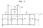
- FIG. 3 illustrates an equivalent circuit model corresponding to the tunable DBR laser illustrated in Figure 2.
- tuning section 212 is illustrated as a parallel capacitance 360 and resistance 362 connected in series with resistance 363 (representing the resistance of the cladding semiconductor).
- Resistance 364 represents the impedance of the circuit driving the tuning section, i.e., an external load.
- the coupling 366 between tuning section 212 and the modulator section 230 is functionally equivalent to a parallel capacitance 368/resistance 370 as shown.
- the modulator section 230 comprises a capacitive load as shown.
- Resistance 372 comprises a chip resistor termination located close to the laser chip to avoid back reflections, and resistance 374 connected in series with the voltage source represents the drive impedance of the voltage source.
- the shunt capacitance of the present invention is illustrated by shunt capacitor 250.
- a value of C>1000 pF for shunt capacitor 250 will give a cross-talk induced value of chirp of less than 0.2 A at 1 GHz.
- Typical values for shunt capacitor 250 range from 100 pF to 100000 pF, depending on the level of chirp reduction desired or required.
- the impedance of the shunt capacitance should be small as compared to the impedance of the coupling 366 between the modulator section 230 and the tuning section 212 over the frequency range of interest.
- shunt capacitor 250 This general requirement places two limitations on the shunt capacitor: its capacitive value should be much larger than that of capacitance 368, so as to shunt high frequencies, and it should be large enough to have a much lower impedance than resistance 370 at lower frequencies.
- the upper limit on the value of shunt capacitor 250 is determined by physical size limitations of the design itself, and the departure of capacitive behavior at high frequencies due to inductive components in the structure of the capacitance.
- the shunt capacitor 250 comprises a capacitor in the 500 - 1,500 pF range. While any capacitor in the range of 100-100,000 pF will suffice, the use of a capacitor in the 500 - 1500 pF range strikes a balance between the desire to shunt high frequencies (i.e., a 1000 pF capacitor is generally much larger in terms of capacitance than the capacitance of the coupling between the tuning section 212 and a modulator section 230, thus shunting high frequencies) and the desire to have good capacitive shunting over a broad frequency range (i.e., high value capacitors tend to deviate from capacitive behavior at high frequencies due to lead inductances and internal resistance).
- a capacitor in the 500 - 1500 pF range strikes a balance between the desire to shunt high frequencies (i.e., a 1000 pF capacitor is generally much larger in terms of capacitance than the capacitance of the coupling between the tuning section 212 and a modulator section 230, thus
- the shunt capacitor is mounted as closely as possible to the laser section 210, generally within a small fraction of an electrical wavelength at the highest frequency of interests, e.g., for 10 Gb/s modulation, at least within a centimeter, and preferably a millimeter or two of the laser section 210.
- any resonance due to bond wires and a capacitor is well beyond one GHz.
- the capacitor 250 suppresses virtually all electrical cross-talk and passes only the DC component of the tuning current.
- the shunt capacitor may be integrated into the substrate on which the tuning section and modulation section are fabricated.
- Fig. 4 illustrates an example of this embodiment, in which shunt capacitor 450, gain section 414, tuning section 412, and modulation section 430 are all integrally formed on substrate 460.
- the fabrication can be performed using conventional fabrication methods; the actual technique used does not, in and of itself, constitute a novel aspect of the present invention.
Landscapes
- Physics & Mathematics (AREA)
- Electromagnetism (AREA)
- Optics & Photonics (AREA)
- Engineering & Computer Science (AREA)
- Computer Networks & Wireless Communication (AREA)
- Signal Processing (AREA)
- Condensed Matter Physics & Semiconductors (AREA)
- General Physics & Mathematics (AREA)
- Nonlinear Science (AREA)
- Semiconductor Lasers (AREA)
- Optical Communication System (AREA)
Applications Claiming Priority (2)
| Application Number | Priority Date | Filing Date | Title |
|---|---|---|---|
| US60679500A | 2000-06-28 | 2000-06-28 | |
| US606795 | 2000-06-28 |
Publications (1)
| Publication Number | Publication Date |
|---|---|
| EP1168534A2 true EP1168534A2 (de) | 2002-01-02 |
Family
ID=24429484
Family Applications (1)
| Application Number | Title | Priority Date | Filing Date |
|---|---|---|---|
| EP01115077A Withdrawn EP1168534A2 (de) | 2000-06-28 | 2001-06-21 | Verfahren und Vorrichtung zur Verringerung von elektrischen Übersprechungsstörungen und Wellenlängen-chirp für einen Laser mit verteiltem Bragg-Reflektor |
Country Status (4)
| Country | Link |
|---|---|
| EP (1) | EP1168534A2 (de) |
| JP (1) | JP2002076508A (de) |
| CN (1) | CN1332531A (de) |
| CA (1) | CA2350092A1 (de) |
Cited By (1)
| Publication number | Priority date | Publication date | Assignee | Title |
|---|---|---|---|---|
| GB2409570A (en) * | 2003-10-10 | 2005-06-29 | Agilent Technologies Inc | A semiconductor optoelectronic component including a distributed Bragg reflector and electro-absorption modulator |
Families Citing this family (2)
| Publication number | Priority date | Publication date | Assignee | Title |
|---|---|---|---|---|
| US7412172B2 (en) * | 2003-12-04 | 2008-08-12 | International Business Machines Corporation | Impedance matching circuit with simultaneous shielding of parasitic effects for transceiver modules |
| CN116318416A (zh) * | 2023-02-13 | 2023-06-23 | 武汉华工正源光子技术有限公司 | 一种差分驱动eml光组件 |
-
2001
- 2001-05-23 CA CA002350092A patent/CA2350092A1/en not_active Abandoned
- 2001-06-21 JP JP2001187912A patent/JP2002076508A/ja active Pending
- 2001-06-21 EP EP01115077A patent/EP1168534A2/de not_active Withdrawn
- 2001-06-28 CN CN01122644A patent/CN1332531A/zh active Pending
Cited By (2)
| Publication number | Priority date | Publication date | Assignee | Title |
|---|---|---|---|---|
| GB2409570A (en) * | 2003-10-10 | 2005-06-29 | Agilent Technologies Inc | A semiconductor optoelectronic component including a distributed Bragg reflector and electro-absorption modulator |
| GB2409570B (en) * | 2003-10-10 | 2007-02-14 | Agilent Technologies Inc | Optoelectronic device having a discrete bragg reflector and an electro-absorption modulator |
Also Published As
| Publication number | Publication date |
|---|---|
| JP2002076508A (ja) | 2002-03-15 |
| CA2350092A1 (en) | 2001-12-28 |
| CN1332531A (zh) | 2002-01-23 |
Similar Documents
| Publication | Publication Date | Title |
|---|---|---|
| US7133576B2 (en) | Traveling-wave optoelectronic wavelength converter | |
| US6437899B1 (en) | Opto-electric conversion semiconductor device | |
| US7869473B2 (en) | Directly modulated laser with isolated modulated gain electrode for improved frequency modulation | |
| US7263244B2 (en) | Optical modulator | |
| US12265286B2 (en) | Broadband electro-absorption optical modulator using on-chip RF input signal termination | |
| US7031612B2 (en) | Optical transponders and transceivers | |
| EP0702436B1 (de) | Lasermodul mit Impedanzanpassungstransformator | |
| US7031558B2 (en) | Low-pass filter transmission line with integral electroabsorption modulator | |
| CN100546132C (zh) | 光调制器模块 | |
| CN100354702C (zh) | 光调制器激励电路 | |
| US8498543B2 (en) | Dispersion tolerant optical system and method | |
| US5781578A (en) | Optical semiconductor device | |
| WO2021210177A1 (ja) | 光半導体チップ | |
| EP1168534A2 (de) | Verfahren und Vorrichtung zur Verringerung von elektrischen Übersprechungsstörungen und Wellenlängen-chirp für einen Laser mit verteiltem Bragg-Reflektor | |
| KR20130056470A (ko) | 송신용 광 모듈 | |
| JP2019033116A (ja) | 半導体光集積素子 | |
| US6990256B2 (en) | Segmented modulator for high-speed opto-electronics | |
| CN112993753B (zh) | 一种单片集成波导装置及其集成半导体芯片 | |
| JP3422279B2 (ja) | 光変調器及び光通信用光源並びにそれを用いる光モジュール、光通信システム | |
| US7570681B2 (en) | Multisectional laser | |
| US20250316956A1 (en) | Differentially-driven electro-absorption modulator | |
| JP2004273584A (ja) | 光半導体素子用駆動回路及び駆動モジュール |
Legal Events
| Date | Code | Title | Description |
|---|---|---|---|
| PUAI | Public reference made under article 153(3) epc to a published international application that has entered the european phase |
Free format text: ORIGINAL CODE: 0009012 |
|
| AK | Designated contracting states |
Kind code of ref document: A2 Designated state(s): AT BE CH CY DE DK ES FI FR GB GR IE IT LI LU MC NL PT SE TR |
|
| AX | Request for extension of the european patent |
Free format text: AL;LT;LV;MK;RO;SI |
|
| STAA | Information on the status of an ep patent application or granted ep patent |
Free format text: STATUS: THE APPLICATION IS DEEMED TO BE WITHDRAWN |
|
| 18D | Application deemed to be withdrawn |
Effective date: 20040103 |