EP1168486A1 - Converter for satellite broadcast reception - Google Patents
Converter for satellite broadcast reception Download PDFInfo
- Publication number
- EP1168486A1 EP1168486A1 EP01303343A EP01303343A EP1168486A1 EP 1168486 A1 EP1168486 A1 EP 1168486A1 EP 01303343 A EP01303343 A EP 01303343A EP 01303343 A EP01303343 A EP 01303343A EP 1168486 A1 EP1168486 A1 EP 1168486A1
- Authority
- EP
- European Patent Office
- Prior art keywords
- waveguide
- converter
- probe
- broadcast reception
- satellite broadcast
- Prior art date
- Legal status (The legal status is an assumption and is not a legal conclusion. Google has not performed a legal analysis and makes no representation as to the accuracy of the status listed.)
- Withdrawn
Links
- 239000000523 sample Substances 0.000 claims abstract description 64
- 238000005452 bending Methods 0.000 claims abstract description 19
- 239000004020 conductor Substances 0.000 claims description 43
- 238000003780 insertion Methods 0.000 claims description 17
- 230000037431 insertion Effects 0.000 claims description 17
- 239000000463 material Substances 0.000 abstract description 3
- 238000010586 diagram Methods 0.000 description 5
- PXHVJJICTQNCMI-UHFFFAOYSA-N Nickel Chemical compound [Ni] PXHVJJICTQNCMI-UHFFFAOYSA-N 0.000 description 4
- NLYAJNPCOHFWQQ-UHFFFAOYSA-N kaolin Chemical compound O.O.O=[Al]O[Si](=O)O[Si](=O)O[Al]=O NLYAJNPCOHFWQQ-UHFFFAOYSA-N 0.000 description 4
- 229910052782 aluminium Inorganic materials 0.000 description 3
- XAGFODPZIPBFFR-UHFFFAOYSA-N aluminium Chemical compound [Al] XAGFODPZIPBFFR-UHFFFAOYSA-N 0.000 description 3
- 229910052751 metal Inorganic materials 0.000 description 3
- 239000002184 metal Substances 0.000 description 3
- 230000010287 polarization Effects 0.000 description 3
- 229910001369 Brass Inorganic materials 0.000 description 2
- YCKRFDGAMUMZLT-UHFFFAOYSA-N Fluorine atom Chemical compound [F] YCKRFDGAMUMZLT-UHFFFAOYSA-N 0.000 description 2
- 239000004698 Polyethylene Substances 0.000 description 2
- 239000004809 Teflon Substances 0.000 description 2
- 229920006362 Teflon® Polymers 0.000 description 2
- HCHKCACWOHOZIP-UHFFFAOYSA-N Zinc Chemical compound [Zn] HCHKCACWOHOZIP-UHFFFAOYSA-N 0.000 description 2
- 239000010951 brass Substances 0.000 description 2
- 238000004512 die casting Methods 0.000 description 2
- 229910052731 fluorine Inorganic materials 0.000 description 2
- 239000011737 fluorine Substances 0.000 description 2
- 238000004519 manufacturing process Methods 0.000 description 2
- 229910052759 nickel Inorganic materials 0.000 description 2
- 230000002093 peripheral effect Effects 0.000 description 2
- -1 polyethylene Polymers 0.000 description 2
- 229920000573 polyethylene Polymers 0.000 description 2
- 229920005989 resin Polymers 0.000 description 2
- 239000011347 resin Substances 0.000 description 2
- 239000011265 semifinished product Substances 0.000 description 2
- 229910000679 solder Inorganic materials 0.000 description 2
- 229910052725 zinc Inorganic materials 0.000 description 2
- 239000011701 zinc Substances 0.000 description 2
- RYGMFSIKBFXOCR-UHFFFAOYSA-N Copper Chemical compound [Cu] RYGMFSIKBFXOCR-UHFFFAOYSA-N 0.000 description 1
- 238000005253 cladding Methods 0.000 description 1
- 239000000470 constituent Substances 0.000 description 1
- 229910052802 copper Inorganic materials 0.000 description 1
- 239000010949 copper Substances 0.000 description 1
- 238000005520 cutting process Methods 0.000 description 1
- 230000000694 effects Effects 0.000 description 1
- 239000007769 metal material Substances 0.000 description 1
- 238000004080 punching Methods 0.000 description 1
Images





Classifications
-
- H—ELECTRICITY
- H04—ELECTRIC COMMUNICATION TECHNIQUE
- H04N—PICTORIAL COMMUNICATION, e.g. TELEVISION
- H04N7/00—Television systems
- H04N7/20—Adaptations for transmission via a GHz frequency band, e.g. via satellite
-
- H—ELECTRICITY
- H01—ELECTRIC ELEMENTS
- H01P—WAVEGUIDES; RESONATORS, LINES, OR OTHER DEVICES OF THE WAVEGUIDE TYPE
- H01P5/00—Coupling devices of the waveguide type
- H01P5/08—Coupling devices of the waveguide type for linking dissimilar lines or devices
- H01P5/10—Coupling devices of the waveguide type for linking dissimilar lines or devices for coupling balanced lines or devices with unbalanced lines or devices
- H01P5/103—Hollow-waveguide/coaxial-line transitions
Definitions
- the present invention relates to a converter for satellite broadcast or communication reception to receive a circularly polarized wave comprising a vertically polarized wave and a horizontally polarized wave.
- FIG. 13 is a perspective view of the conventional converter for satellite broadcast reception
- FIG. 14 is a sectional view taken on line 14-14 in FIG. 13
- FIG. 15 is an enlarged view of a principal portion, explaining a mounted state of a probe
- FIG. 16 is an enlarged view of a principal portion, showing a mounted state of a circuit board.
- a housing 31 and a waveguide 32 are formed integrally using a metallic material such as die-cast aluminum or zinc.
- the housing 31, which is formed in a generally rectangular box shape, comprises a bottom wall 31a, side walls 31b formed upright so as to enclose the bottom wall 31a while allowing an upper side to be open, a receptacle portion 31c enclosed with the side walls 31b, a vertical through hole 31d formed in a position close to one end portion of the bottom wall 31a, and stepped portions 31e formed by cutting out peripheral edges of upper ends of the side walls 31b.
- the waveguide 32 is formed in a cylindrical shape relatively small in diameter and is projected from the bottom wall 31a at the position of the through hole 31d.
- the waveguide 32 comprises a generally cylindrical portion 32b having an opening 32a for introducing a polarized wave, a hollow portion 32c formed centrally in the longitudinal direction of the cylindrical portion, and a holding portion 32d formed as a semi-cylindrical recess within the cylindrical portion 32b, the holding portion 32d extending toward the opening 32a from a peripheral edge position of the through hole 31d formed in the housing 31, as shown in FIG. 15.
- a probe 33 for catching a horizontally polarized wave is made up of a cylindrical insulating portion 33a formed of, for example, a fluorine resin, polyethylene, or Teflon, and a linear central conductor 33b piercing through the center of the insulating portion 33a and formed of a metal such as brass or nickel.
- the central conductor 33b has one end portion 33c which is bent approximately at right angles and an opposite end portion 33d which is rectilinear.
- the insulating portion 33a of the probe 33 is press-fitted into the holding portion 32d of the waveguide 32 and is thereby mounted to the waveguide.
- the opposite end portion 33d of the central conductor 33b is projected to the receptacle portion 31c side of the housing 31, while the bent one end portion 33c is projected up to the center of the hollow portion 32c of the waveguide 32.
- a single rectangular circuit board 34 formed by an insulating board comprises a thin flat plate portion 34a, three vertical through holes 34b formed near a side edge of the flat plate portion 34a, bridge portions 34d and 34e which are formed in T shape, and a small hole 34c formed near the through hole 34b.
- a copper-clad earth conductor 35 is formed on a lower surface of the circuit board 34 except the lower surface portion where the bridge portion 34e is formed.
- a lower surface of the bridge portion 34d functions as a short-circuit rod for the probe 33.
- a probe 36 for catching a vertically polarized wave is formed as a conductive pattern on an upper surface of the flat plate portion, extending from an intersecting point of the bridge portions 34d and 34e toward the flat plate portion 34a, and is connected to a circuit pattern (not shown) formed on an upper surface of the flat plate portion 34a.
- the through hole 31d formed in the housing 31 and the through holes 34b formed in the flat plate portion 34a are opposed to each other and the opposite end portion 33d of the central conductor 33b of the probe 33 is inserted through the hole 34c formed in the flat plate portion 34a.
- the circuit board 34 of the above configuration placed on the bottom wall 31a of the housing 31 and is fixed by a suitable means.
- the opposite end portion 33d of the central conductor 33b projected above the circuit board 34 is soldered to a circuit pattern by solder 37.
- a short-circuit wall 38 is formed in a box shape using a metal such as die-cast aluminum or zinc and is secured to the circuit board 34 by a desired means, e.g., caulking, so as to cover the through holes 34b formed in the circuit board.
- a bottom portion 38a of the short-circuit wall 38 functions as a short-circuit portion for the probe 36.
- a cover 39 which is constituted by a single rectangular metallic plate, is placed on the stepped portions 31e of the side walls 31b of the housing 31 and is fixed by a suitable means.
- the receptacle portion 31c of the housing 31 is hermetically sealed and the interior thereof is shielded electrically.
- the waveguide 32 and the holding portion 32d are formed integrally by die-casting aluminum for example, the material cost is high and it takes a considerable time for the manufacture, that is, the productivity is poor.
- the insulating portion 33a of the probe 33 be press-fitted into the holding portion 32d of the waveguide 32; besides, the press-fitting work is performed in the hollow portion 32c which is narrow. Consequently, a considerable time is required for the manufacture, that is, the productivity is poor.
- a converter for satellite broadcast reception comprising a box-shaped metallic housing, a cylindrical waveguide, and a probe attached to the waveguide, the probe having a cylindrical insulating portion and a central conductor piercing through a central part of the insulating portion, the waveguide being formed by bending a metallic plate and being integrally provided with a holding portion positioned outside the waveguide to hold the insulating portion of the probe.
- the insulating portion of the probe is held grippingly by both an outer surface of the waveguide and the holding portion.
- the holding portion is provided with a retaining piece for locking a free end side of the holding portion to the waveguide.
- the holding portion covers the probe throughout the whole in the longitudinal direction of the insulating portion which is exposed from the waveguide.
- the holding portion covers the probe throughout the whole in the longitudinal direction of the central conductor which is exposed from the waveguide.
- the insulating portion with the central conductor installed therein is formed with a slot in the longitudinal direction thereof, and one end portion of the central conductor is bent along the slot.
- an outer surface of the insulating portion of the probe includes a flat surface, and the probe is held by the holding portion in an abutted state of the flat surface against an outer surface of the waveguide.
- the flat surface formed as a part of the outer surface of the insulating portion is perpendicular to an extending direction of one end of the central conductor, and the probe is held by the holding portion in an abutted state of the flat surface against the outer surface of the waveguide.
- an insertion hole for insertion therein of the central conductor is formed in the waveguide, and with the central conductor inserted into the insertion hole, the insulating portion of the probe is placed on the outer surface of the waveguide so as to straddle the insertion hole.
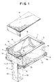
- FIG. 1 is an exploded perspective view of the converter
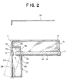
- FIG. 2 is an exploded sectional view thereof
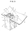
- FIG. 3 is an explanatory diagram showing in what state a waveguide is mounted to a circuit board
- FIG. 4 is a developed view of semi-finished components, showing how to assemble the converter
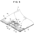
- FIG. 5 is an enlarged view of the circuit board
- FIGS. 6 and 7 are explanatory diagrams showing in what state a probe is mounted
- FIG. 8 is a perspective view showing a modified example of a holding member
- FIG. 9 is a top view thereof.
- the converter for satellite broadcast reception comprises a housing 1, a waveguide 2 and a short-circuit wall 7 which are connected together and formed integrally by bending a single thin metallic plate.
- the housing 1 which is formed in a box shape using a thin metallic plate, comprises a ⁇ -shaped upper wall 1e having a central rectangular hole 1g and a brim portion formed along an outer periphery of the hole 1g, and side walls 1a, 1b, 1c and 1d formed upright by bending the upper wall 1e on the four sides of the upper wall.
- the side walls 1a to 1d are integrally connected to the upper wall 1e.
- An upper portion of the side wall 1d opposed to the side wall 1c is formed with a large cutout portion 1h which is contiguous to the hole 1g.
- a plurality of generally ⁇ -shaped engaging pieces 1f are formed at a lower end of each of the side walls 1a, 1b and 1c.
- the waveguide 2 which is formed in the shape of a rectangular parallelepiped using a thin metallic plate, comprises a side plate portion 2a connected to the side wall 1d of the housing 1 through a connecting portion 1i and extending downward, side plate portions 2b and 2d formed by bending the metallic plate at right angles on both sides of the side plate portion 2a, a side plate portion 2c formed by bending the metallic plate at right angles from the side plate portion 2b, the side plate portion 2c being connected to the side plate portion 2d and opposed to the side plate portion 2a, a hollow portion 2e formed by being enclosed with the side plate portions 2a to 2d, and end portions 2f as free ends of the side plate portions 2b to 2d exclusive of the connecting portion 1i. As shown in FIGS.
- two generally ⁇ -shaped retaining pieces 2g are formed at the end 2f of the side plate portion 2c opposed to the side plate portion 2a which is connected to the housing 1 .
- a generally rectangular engaging hole 3 is formed in the boundary between the side plate portions 2a and 2d, and an insertion hole 4 comprising a circular hole 4a and a rectangular hole 4b is formed in the side plate portion 2d at a position close to the engaging hole 3.
- a bending facilitating means 5 such as a cut-in portion.
- the waveguide 2 when formed by bending a thin metallic plate, is projected downward vertically from the housing 1, as shown in FIG. 1, and it is tiltable relative to the housing 1, centered on the bending facilitating means 5, as indicated with a dotted line in FIG. 2.
- a holding member 6 is formed so as to be positioned outside the waveguide 2 and it is connected to the side plate portion 2c through a connecting portion 2h.
- the holding member 6 comprises a flat plate-like base portion 6a, a semi-cylindrical embracing portion 6b formed centrally of the base portion 6a, and a generally ⁇ - shaped retaining piece 6c formed by being bent on a free end side of the base portion 6a.
- the holding member 6 can be bent from the side plate portion 2c. When the holding member 6 is bent so as to become opposed to the side plate portion 2d, the retaining piece 6c can be engaged with the engaging hole 3.
- the short-circuit wall 7 which is formed in a box shape using a thin metallic plate, comprises a lid portion 7a connected to the side wall 1d of the housing 1 and formed by being bent at right angles from the side wall 1d, side portions 7b, 7c and 7d formed by being bent downward on the side opposed to the side wall 1d, and a cavity 7e enclosed with the lid portion 7a, side portions 7b - 7d and side wall 1d.
- the short-circuit wall 7 is positioned within the housing 1 so that its cavity 7e is opposed to the hollow portion 2e of the waveguide 2.
- a probe 8 for catching a horizontally polarized wave is made up of a cylindrical L-shaped insulating portion 8a formed of, for example, a fluorine resin, polyethylene or Teflon and a linear central conductor 8b formed mainly using such a metal as brass or nickel and piercing through a central part of the insulating portion 8a.
- the central conductor 8b has one end portion 8c which is bent at right angles together with the insulating portion 8a and an opposite end portion 8d positioned perpendicularly to the one end portion 8c.
- one end portion of the L-shaped insulating portion 8a of the probe 8 is fitted into the circular hole 4a as a constituent of the insertion hole 4 formed in the side plate portion 2d of the waveguide 2, while the opposite end portion of the insulating portion 8a exposed from the waveguide 2 is held while being gripped by both an outer surface of the side plate portion 2d of the waveguide and the embracing portion 6b of the holding member 6.
- the opposite end portion of the insulating portion 8a exposed from the waveguide 2 is covered with the embracing portion 6b of the holding member 6 throughout the whole thereof in its longitudinal direction and so is the central conductor 8b exposed from the waveguide 2.
- the opposite end portion 8d of the central conductor 8b projects to the housing 1 side, while the bent one end portion 8c projects to a central part of the hollow portion 2e of the waveguide 2.
- a rectangular circuit board 9 which is formed by a single insulating board, comprises a thin flat plate portion 9a, a cutout portion 9b formed in one side edge of the flat plate portion 9a, three generally rectangular, vertical through holes 9c formed near the cutout portion 9b, bridge portions 9g and 9h defined in T shape by the through holes 9c, a small hole 9d formed near the through holes 9c, two first engaging holes 9e formed in positions near the through holes 9c and opposed to the cutout portion 9b, and a plurality of second engaging holes 9f formed in marginal positions of the flat plate portion 9a.
- a copper-clad earth conductor 10 is formed on a lower surface of the flat plate portion 9a throughout the whole of the lower surface exclusive of the bridge portion 9h.
- a probe 11 for catching a vertically polarized wave is formed by a conductive pattern on an upper surface of the bridge portion 9h so as to extend from an intersecting point of the bridge portions 9g and 9h up to the flat plate portion 9a of the circuit board 9 and is connected to a wiring pattern (not shown) formed on an upper surface of the flat plate portion 9a.
- a band-like earth pattern 12 is formed by copper cladding on the upper surface of the flat plate portion 9a so as to surround the through holes 9c and in a connected state with the earth conductor 10 through a plurality of through holes 12a formed through the circuit board 9.
- the upper surface of the flat plate portion 9a of the circuit board 9 thus constructed is brought into abutment against lower ends of the side walls 1a - 1d and the circuit board 9 is held grippingly by both the side wall lower ends and the end portions 2f of the waveguide 2 against which a lower surface of the flat plate portion 9a is in abutment.
- the retaining pieces 2g of the waveguide 2 and the first engaging holes 9e formed in the circuit board 9 are engaged with each other and the engaging pieces 1f of the housing 1 and the second engaging holes 9f formed in the circuit board are also engaged with each other to effect holding of the circuit board.
- the upper surface of the flat plate portion 9a of the circuit board 9 comes into abutment against lower ends of the side portions 7b - 7d of the short-circuit wall 7 and the side plate portion 2a of the waveguide 2 is fitted in the cutout portion 9b of the flat plate portion 9a.
- the through holes 9c formed in the circuit board 9 is opposed to the hollow portion 2e of the waveguide 2 and the cavity 7e of the short-circuit wall 7, the side portions 7b - 7d of the short-circuit wall 7 are abutted against the earth pattern 12, and the opposite end portion 8d of the central conductor 8b in the probe 8 is inserted through the hole 9d formed in the flat plate portion 9a.
- the opposite end portion 8d of the central conductor 8b projecting above the circuit board 9 is soldered by solder 13 and is connected to a wiring pattern formed on the circuit board.
- the through holes 9c formed in the circuit board 9 are positioned inside the waveguide 2 and also inside the short-circuit wall 7 and a lower surface of the circuit board except the through holes 9c is shielded by the earth conductor 10.
- An L-shaped cover 14 which is constituted by a single rectangular metallic plate, is fitted in a fitting portion constituted by both side wall 1d and upper wall 1e of the housing 1 and is fixed by a suitable means. In this way the interior of the housing 1 is put in a hermetically sealed and electrically shielded state.
- the converter for satellite broadcast reception is constructed as above. Now, a description will be given about how to assemble the converter.
- the housing 1 which comprises the upper wall 1e formed with the central hole 1g and the cutout portion 1h and the side walls 1a - 1d extending on all sides from the upper wall 1e
- the waveguide 2 which is formed outside the housing 1 and which comprises the side plate portion 2a extending from the side wall 1d, the side plate portions 2b and 2c extending contiguously from one side of the side plate portion 2a, the side plate portion 2d extending from the opposite side of the side plate portion 2a, and the holding portion 6 extending outward from the side plate portion 2c through the connecting portion 2h
- the short-circuit wall 7 which comprises the lid portion 7a extending from the side wall 1d opposedly to the side plate portion 2a and the side portions 7b - 7d extending in three directions from the lid portion 7a, the short-circuit wall 7 spanning both hole 1g and cutout portion
- the housing 1a - 1d In the semi-finished product 15, by bending the side walls 1a - 1d at right angles in the respective positions indicated with dotted lines A, there is formed the housing 1. Likewise, by bending the side plate portions 2b - 2d at right angles in the respective positions indicated with dotted lines B and connecting the side plate portions 2c and 2d with each other, there is formed the waveguide 2. Further, by bending the lid portion 7a at right angles in the position of a dotted line C and by bending the side portions 7b - 7d in the positions of dotted lines D, there is formed the short-circuit wall 7. As a result, there is formed such an entire shape as shown in FIG. 1.
- the waveguide 2 suspended vertically from the housing 1 is tilted outward from the bending facilitating means 5 as indicated with a dotted line, allowing the circuit board 9 to be positioned between the housing and the waveguide, and thereafter the waveguide 2 is restored to its vertical state to pinch the circuit board 9 between the housing 1 and the waveguide 2.
- This pinching operation is performed by first mounting the circuit board 9 to the underside of the housing 1 while fitting the engaging pieces 1f of the housing 1 into the second engaging holes 9f formed in the circuit board and by subsequently bringing the retaining pieces 2g formed on a free end-side end portion 2f of the waveguide 2 into engagement with the first engaging holes 9e formed in the circuit board 9, as shown in FIG. 3.
- the circuit board 9 is pinched and held firmly by such engagements.
- the probe 8 is fitted in the insertion hole 4 by turning the probe in the direction of arrow from its state shown in FIG. 6 until the one end portion 8c of the central conductor 8b is positioned within the hollow portion 2e and by allowing the insulating portion 8a to be engaged in the circular hole 4a.
- the holding portion 6 is bent from the connecting portion 2h and the retaining piece 6c formed on a free end side of the holding portion 6 is locked to the engaging hole 3, thereby holding the insulating portion 8a grippingly between the embracing portion 6b and the side plate portion 2d and so holding the probe 8.
- Two polarized waves orthogonal to each other are introduced through the waveguide 2 into the hollow portion 2e of the waveguide.
- a horizontally polarized wave is reflected by a part of the earth conductor 10 formed on the back of the bridge portion 9g and is caught by the one end portion 8c of the probe 8 projecting into the hollow portion 2e, while a vertically polarized wave is reflected by the lid portion 7a of the short-circuit wall 7 and is caught by the probe 11 formed on the upper surface of the bridge portion 9h.
- the horizontally polarized wave caught by the probe 8 is transmitted as a horizontal polarization signal to an electric circuit on the circuit board 9 through the central conductor 8b.
- the vertically polarized wave caught by the probe 11 is transmitted as a vertical polarization signal to the electric circuit on the circuit board 9, which circuit in turn combines the polarization signals transmitted from the probes.
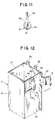
- FIGS. 10 to 12 illustrate a converter for satellite broadcast reception according to the second embodiment of the present invention, of which FIG. 10 is a perspective view of a probe used in the converter, FIG. 11 is a plan view thereof, and FIG. 12 is a perspective view showing in what state the probe is mounted in the converter.
- An insulating portion 8a of a probe 8 has a slot 8c formed longitudinally and a flat surface 8d formed on an outer surface of the insulating portion.
- a central conductor 8b is press-fitted into the insulating portion 8a and one end thereof is bent at right angles along the slot 8c and is projected outward from the slot.
- the flat surface 8d is formed at a position perpendicular to the extending direction of the bent one end of the central conductor 8b.
- the bent one end of the central conductor 8b is inserted into the insertion hole 4 of the waveguide 2 and the flat surface 8c of the insulating portion 8a is placed on an outer surface of the waveguide 2 in such a manner that the insulating portion 8a straddles the insertion hole 4.
- a holding portion 6 is bent to push the insulating portion 8a against the outer surface of the waveguide 2, whereby the probe 8 is mounted.
- the holding portion 6 may be in a bent state from the connecting portion 2h, not having a retaining piece, and the insulating portion 8a may be held by such a holding portion.
- the holding portion 6 may be formed as in FIG. 9, in which the insulating portion 8a is embraced and held substantially throughout the whole circumferential surface thereof by only the holding portion 6.
- the bending facilitating means 5 is not limited to such a cut-in portion as referred to in the above embodiments, but it may be perforations.
- the waveguide is formed by bending a metallic plate and is integrally provided with a holding portion which is positioned outside the waveguide, and an insulating portion of a probe is held by the holding portion. Therefore, the probe can be held easily by the waveguide and hence it is possible to improve the productivity.
- the waveguide is constituted by a single thin metallic plate, it is not necessary to use a mold and the material cost is reduced, thus permitting the provision of a less expensive converter for satellite broadcast reception.
- the insulating portion of the probe is held in a pinched state by both an outer surface of the waveguide and the holding portion, it is possible to hold the probe positively and hence possible to provide a more reliable converter for satellite broadcast reception.
- the holding portion is provided with a retaining piece for locking a free end side of the holding portion to the waveguide, the probe can be held in a simple and positive manner and the free end of the holding portion can be fixed surely to the waveguide, thus making it possible to provide a converter for satellite broadcast reception with no likelihood of reversion of the holding portion from its bent state.
- the holding portion covers the probe throughout the whole in the longitudinal direction of the insulating portion exposed from the waveguide, the probe can be held positively and it is possible to provide a highly reliable converter for satellite broadcast reception.
- the holding portion covers the probe throughout the whole in the longitudinal direction of the central conductor exposed from the waveguide, not only the holding portion functions to shield the probe but also it makes the probe difficult to be deformed against an external force, thus permitting the provision of a converter for satellite broadcast reception which is little deformed.
- the insulating portion with the central conductor installed therein is formed with a longitudinal slot and one end portion of the central conductor is bent along the slot, bending of the central conductor can be done uniformly and it is possible to provide a converter for satellite broadcast reception which permits an accurate bending.
- the outer surface of the insulating portion is formed with a flat surface perpendicular to the extending direction of one end of the central conductor and the probe is held by the holding portion in an abutted state of the flat surface against the outer surface of the waveguide, the insulating portion and the central conductor can be installed accurately and it is possible to provide a converter for satellite broadcast reception superior in assemblability.
- the waveguide is formed with an insertion hole for insertion therein of the central conductor and in an inserted state of the central conductor into the insertion hole the insulating portion is rested on the outer surface of the waveguide so as to straddle the insertion hole, the insulating portion can be stably rested on the outer surface of the waveguide and it is possible to provide a converter for satellite broadcast reception with the probe installed therein firmly.
Landscapes
- Physics & Mathematics (AREA)
- Astronomy & Astrophysics (AREA)
- General Physics & Mathematics (AREA)
- Engineering & Computer Science (AREA)
- Multimedia (AREA)
- Signal Processing (AREA)
- Waveguide Aerials (AREA)
Abstract
Description
- The present invention relates to a converter for satellite broadcast or communication reception to receive a circularly polarized wave comprising a vertically polarized wave and a horizontally polarized wave.
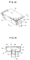
- A conventional converter for satellite broadcast reception will be described below with reference to FIGS. 13 to 16, of which FIG. 13 is a perspective view of the conventional converter for satellite broadcast reception, FIG. 14 is a sectional view taken on line 14-14 in FIG. 13, FIG. 15 is an enlarged view of a principal portion, explaining a mounted state of a probe, and FIG. 16 is an enlarged view of a principal portion, showing a mounted state of a circuit board.
- A
housing 31 and awaveguide 32 are formed integrally using a metallic material such as die-cast aluminum or zinc. Thehousing 31, which is formed in a generally rectangular box shape, comprises abottom wall 31a,side walls 31b formed upright so as to enclose thebottom wall 31a while allowing an upper side to be open, areceptacle portion 31c enclosed with theside walls 31b, a vertical throughhole 31d formed in a position close to one end portion of thebottom wall 31a, and steppedportions 31e formed by cutting out peripheral edges of upper ends of theside walls 31b. Thewaveguide 32 is formed in a cylindrical shape relatively small in diameter and is projected from thebottom wall 31a at the position of thethrough hole 31d. Thewaveguide 32 comprises a generallycylindrical portion 32b having an opening 32a for introducing a polarized wave, ahollow portion 32c formed centrally in the longitudinal direction of the cylindrical portion, and aholding portion 32d formed as a semi-cylindrical recess within thecylindrical portion 32b, theholding portion 32d extending toward the opening 32a from a peripheral edge position of the throughhole 31d formed in thehousing 31, as shown in FIG. 15. - A
probe 33 for catching a horizontally polarized wave is made up of a cylindricalinsulating portion 33a formed of, for example, a fluorine resin, polyethylene, or Teflon, and a linearcentral conductor 33b piercing through the center of theinsulating portion 33a and formed of a metal such as brass or nickel. Thecentral conductor 33b has oneend portion 33c which is bent approximately at right angles and anopposite end portion 33d which is rectilinear. - As shown in FIG. 15, the
insulating portion 33a of theprobe 33 is press-fitted into theholding portion 32d of thewaveguide 32 and is thereby mounted to the waveguide. With theprobe 33 thus mounted, theopposite end portion 33d of thecentral conductor 33b is projected to thereceptacle portion 31c side of thehousing 31, while the bent oneend portion 33c is projected up to the center of thehollow portion 32c of thewaveguide 32. - As shown in FIG. 16, a single
rectangular circuit board 34 formed by an insulating board comprises a thin flat plate portion 34a, three vertical throughholes 34b formed near a side edge of the flat plate portion 34a,bridge portions small hole 34c formed near thethrough hole 34b. A copper-clad earth conductor 35 is formed on a lower surface of thecircuit board 34 except the lower surface portion where thebridge portion 34e is formed. A lower surface of thebridge portion 34d functions as a short-circuit rod for theprobe 33. - A
probe 36 for catching a vertically polarized wave is formed as a conductive pattern on an upper surface of the flat plate portion, extending from an intersecting point of thebridge portions hole 31d formed in thehousing 31 and the throughholes 34b formed in the flat plate portion 34a are opposed to each other and theopposite end portion 33d of thecentral conductor 33b of theprobe 33 is inserted through thehole 34c formed in the flat plate portion 34a. In this state thecircuit board 34 of the above configuration placed on thebottom wall 31a of thehousing 31 and is fixed by a suitable means. Theopposite end portion 33d of thecentral conductor 33b projected above thecircuit board 34 is soldered to a circuit pattern bysolder 37. - A short-
circuit wall 38 is formed in a box shape using a metal such as die-cast aluminum or zinc and is secured to thecircuit board 34 by a desired means, e.g., caulking, so as to cover the throughholes 34b formed in the circuit board. Abottom portion 38a of the short-circuit wall 38 functions as a short-circuit portion for theprobe 36. - A
cover 39, which is constituted by a single rectangular metallic plate, is placed on thestepped portions 31e of theside walls 31b of thehousing 31 and is fixed by a suitable means. Thereceptacle portion 31c of thehousing 31 is hermetically sealed and the interior thereof is shielded electrically. - In the conventional converter for satellite broadcast reception, however, since the
waveguide 32 and theholding portion 32d are formed integrally by die-casting aluminum for example, the material cost is high and it takes a considerable time for the manufacture, that is, the productivity is poor. - Besides, since the
holding portion 32d is formed, the mold used for die casting is complicated and expensive, thus giving rise to the problem that the converter becomes expensive. - Further, it is necessary that the
insulating portion 33a of theprobe 33 be press-fitted into theholding portion 32d of thewaveguide 32; besides, the press-fitting work is performed in thehollow portion 32c which is narrow. Consequently, a considerable time is required for the manufacture, that is, the productivity is poor. - It is an object of the present invention to provide a converter for satellite broadcast reception which is superior in productivity and inexpensive.
- According to the first means adopted by the present invention for solving the above-mentioned problems there is provided a converter for satellite broadcast reception, comprising a box-shaped metallic housing, a cylindrical waveguide, and a probe attached to the waveguide, the probe having a cylindrical insulating portion and a central conductor piercing through a central part of the insulating portion, the waveguide being formed by bending a metallic plate and being integrally provided with a holding portion positioned outside the waveguide to hold the insulating portion of the probe.
- Preferably, the insulating portion of the probe is held grippingly by both an outer surface of the waveguide and the holding portion.
- Preferably, the holding portion is provided with a retaining piece for locking a free end side of the holding portion to the waveguide.
- Preferably, the holding portion covers the probe throughout the whole in the longitudinal direction of the insulating portion which is exposed from the waveguide.
- Preferably, the holding portion covers the probe throughout the whole in the longitudinal direction of the central conductor which is exposed from the waveguide.
- Preferably, the insulating portion with the central conductor installed therein is formed with a slot in the longitudinal direction thereof, and one end portion of the central conductor is bent along the slot.
- Preferably, an outer surface of the insulating portion of the probe includes a flat surface, and the probe is held by the holding portion in an abutted state of the flat surface against an outer surface of the waveguide.
- Preferably, the flat surface formed as a part of the outer surface of the insulating portion is perpendicular to an extending direction of one end of the central conductor, and the probe is held by the holding portion in an abutted state of the flat surface against the outer surface of the waveguide.
- Preferably, an insertion hole for insertion therein of the central conductor is formed in the waveguide, and with the central conductor inserted into the insertion hole, the insulating portion of the probe is placed on the outer surface of the waveguide so as to straddle the insertion hole.
- An embodiment of the present invention, will now be described, by way of example only, with reference to the accompanying diagrammatic drawings, in which:
- FIG. 1 is an exploded perspective view of a converter for satellite broadcast reception according to the first embodiment of the present invention;
- FIG. 2 is an exploded sectional view thereof;
- FIG. 3 is an explanatory diagram showing in what state a waveguide is mounted to a circuit board in the converter of the first embodiment;
- FIG. 4 is a developed view of semi-finished components, showing how to assemble the converter of the first embodiment;
- FIG. 5 is an enlarged view of the circuit board used in the converter of the first embodiment;
- FIG. 6 is an explanatory diagram showing in what state a probe is mounted in the converter of the first embodiment;
- FIG. 7 is an explanatory diagram showing in what state the probe is mounted in the converter of the first embodiment;
- FIG. 8 is a perspective view showing a modified example of a holding member employable in the converter of the first embodiment;
- FIG. 9 is a top view thereof;
- FIG. 10 is a perspective view of a probe used in a converter for satellite broadcast reception according to the second embodiment of the present invention;
- FIG. 11 is a plan view thereof;
- FIG. 12 is a perspective view showing in what state the probe is mounted;
- FIG. 13 is a perspective view of a conventional converter for satellite broadcast reception;
- FIG. 14 is a sectional view taken on line 14-14 in FIG. 13;
- FIG. 15 is an enlarged view of a principal portion, showing in what state a probe is mounted in the conventional converter; and
- FIG. 16 is an enlarged view of a principal portion, showing in what state a circuit board is mounted in the conventional converter.
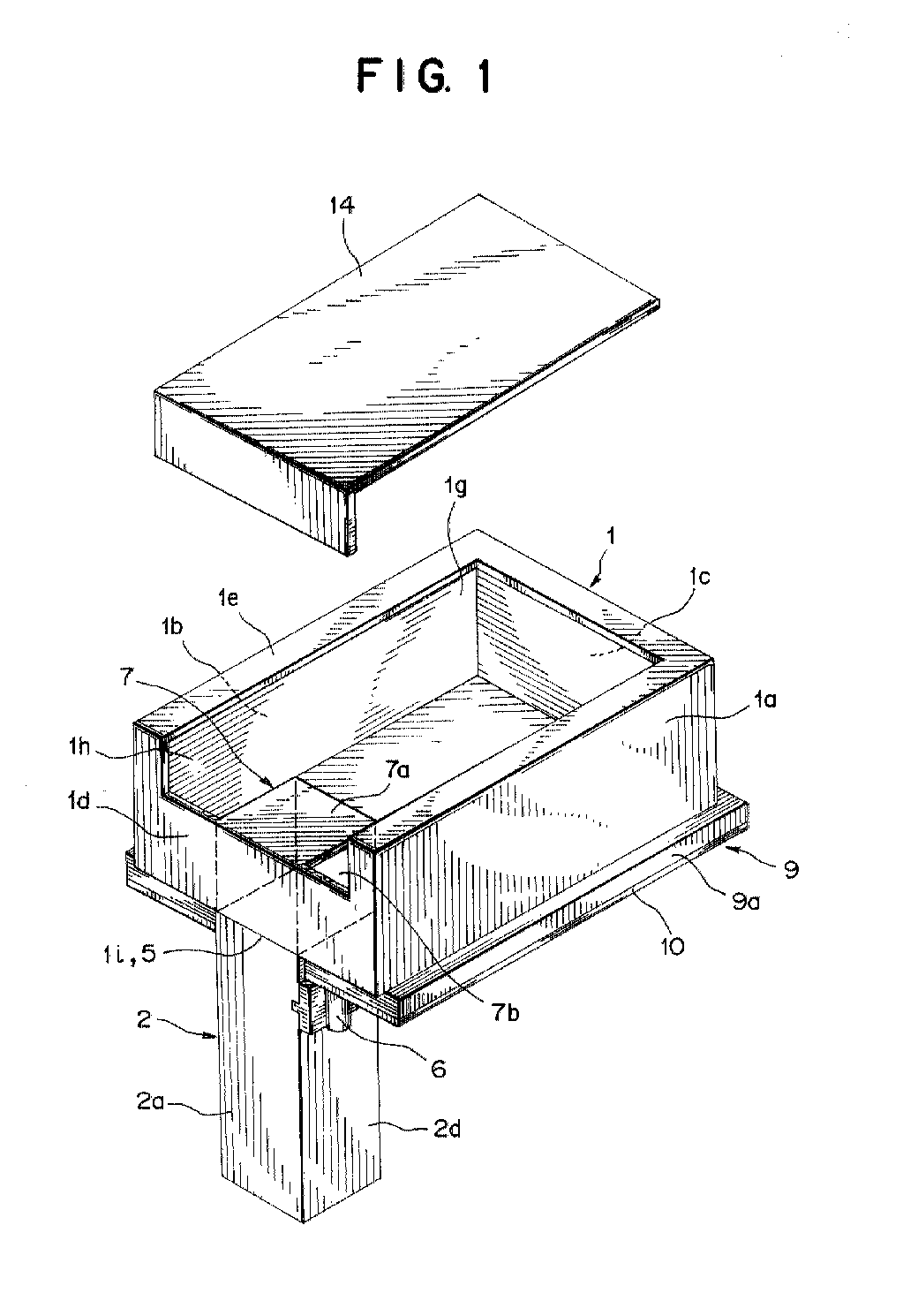
- A converter for satellite broadcast reception according to the first embodiment of the present invention will be described below with reference to FIGS. 1 to 9, of which FIG. 1 is an exploded perspective view of the converter, FIG. 2 is an exploded sectional view thereof, FIG. 3 is an explanatory diagram showing in what state a waveguide is mounted to a circuit board, FIG. 4 is a developed view of semi-finished components, showing how to assemble the converter, FIG. 5 is an enlarged view of the circuit board, FIGS. 6 and 7 are explanatory diagrams showing in what state a probe is mounted, FIG. 8 is a perspective view showing a modified example of a holding member, and FIG. 9 is a top view thereof.
- As shown in FIGS. 1 to 9, the converter for satellite broadcast reception according to the first embodiment of the present invention comprises a
housing 1, awaveguide 2 and a short-circuit wall 7 which are connected together and formed integrally by bending a single thin metallic plate. - The
housing 1, which is formed in a box shape using a thin metallic plate, comprises a ⊐-shapedupper wall 1e having a centralrectangular hole 1g and a brim portion formed along an outer periphery of thehole 1g, andside walls upper wall 1e on the four sides of the upper wall. The side walls 1a to 1d are integrally connected to theupper wall 1e. An upper portion of theside wall 1d opposed to theside wall 1c is formed with alarge cutout portion 1h which is contiguous to thehole 1g. Further, as shown in FIG. 4, a plurality of generally <-shapedengaging pieces 1f are formed at a lower end of each of theside walls - The
waveguide 2, which is formed in the shape of a rectangular parallelepiped using a thin metallic plate, comprises aside plate portion 2a connected to theside wall 1d of thehousing 1 through a connecting portion 1i and extending downward,side plate portions side plate portion 2a, aside plate portion 2c formed by bending the metallic plate at right angles from theside plate portion 2b, theside plate portion 2c being connected to theside plate portion 2d and opposed to theside plate portion 2a, ahollow portion 2e formed by being enclosed with theside plate portions 2a to 2d, andend portions 2f as free ends of theside plate portions 2b to 2d exclusive of the connecting portion 1i. As shown in FIGS. 2 and 3, two generally <-shaped retaining pieces 2g are formed at theend 2f of theside plate portion 2c opposed to theside plate portion 2a which is connected to thehousing 1. Further, as shown in FIG. 4, a generally rectangularengaging hole 3 is formed in the boundary between theside plate portions insertion hole 4 comprising a circular hole 4a and arectangular hole 4b is formed in theside plate portion 2d at a position close to theengaging hole 3. In the connecting portion 1i between theside plate portion 2a and theside wall 1d of thehousing 1 there is formed a bending facilitating means 5 such as a cut-in portion. Thewaveguide 2, when formed by bending a thin metallic plate, is projected downward vertically from thehousing 1, as shown in FIG. 1, and it is tiltable relative to thehousing 1, centered on thebending facilitating means 5, as indicated with a dotted line in FIG. 2. - As shown in FIGS. 3 and 4, a
holding member 6 is formed so as to be positioned outside thewaveguide 2 and it is connected to theside plate portion 2c through a connectingportion 2h. The holdingmember 6 comprises a flat plate-like base portion 6a, asemi-cylindrical embracing portion 6b formed centrally of thebase portion 6a, and a generally <- shapedretaining piece 6c formed by being bent on a free end side of thebase portion 6a. - The holding
member 6 can be bent from theside plate portion 2c. When the holdingmember 6 is bent so as to become opposed to theside plate portion 2d, the retainingpiece 6c can be engaged with the engaginghole 3. - The short-
circuit wall 7, which is formed in a box shape using a thin metallic plate, comprises a lid portion 7a connected to theside wall 1d of thehousing 1 and formed by being bent at right angles from theside wall 1d,side portions side wall 1d, and acavity 7e enclosed with the lid portion 7a,side portions 7b - 7d andside wall 1d. - The short-
circuit wall 7 is positioned within thehousing 1 so that itscavity 7e is opposed to thehollow portion 2e of thewaveguide 2. - As shown in FIG 6, a
probe 8 for catching a horizontally polarized wave is made up of a cylindrical L-shaped insulatingportion 8a formed of, for example, a fluorine resin, polyethylene or Teflon and a linearcentral conductor 8b formed mainly using such a metal as brass or nickel and piercing through a central part of the insulatingportion 8a. Thecentral conductor 8b has oneend portion 8c which is bent at right angles together with the insulatingportion 8a and anopposite end portion 8d positioned perpendicularly to the oneend portion 8c. - As shown particularly in FIGS. 3 and 7, one end portion of the L-shaped insulating
portion 8a of theprobe 8 is fitted into the circular hole 4a as a constituent of theinsertion hole 4 formed in theside plate portion 2d of thewaveguide 2, while the opposite end portion of the insulatingportion 8a exposed from thewaveguide 2 is held while being gripped by both an outer surface of theside plate portion 2d of the waveguide and the embracingportion 6b of the holdingmember 6. At this time, the opposite end portion of the insulatingportion 8a exposed from thewaveguide 2 is covered with the embracingportion 6b of the holdingmember 6 throughout the whole thereof in its longitudinal direction and so is thecentral conductor 8b exposed from thewaveguide 2. - When the
probe 8 is mounted, theopposite end portion 8d of thecentral conductor 8b projects to thehousing 1 side, while the bent oneend portion 8c projects to a central part of thehollow portion 2e of thewaveguide 2. - As shown in FIG. 5, a
rectangular circuit board 9, which is formed by a single insulating board, comprises a thinflat plate portion 9a, acutout portion 9b formed in one side edge of theflat plate portion 9a, three generally rectangular, vertical throughholes 9c formed near thecutout portion 9b,bridge portions holes 9c, asmall hole 9d formed near the throughholes 9c, two first engagingholes 9e formed in positions near the throughholes 9c and opposed to thecutout portion 9b, and a plurality of second engagingholes 9f formed in marginal positions of theflat plate portion 9a. A copper-cladearth conductor 10 is formed on a lower surface of theflat plate portion 9a throughout the whole of the lower surface exclusive of thebridge portion 9h. - A
probe 11 for catching a vertically polarized wave is formed by a conductive pattern on an upper surface of thebridge portion 9h so as to extend from an intersecting point of thebridge portions flat plate portion 9a of thecircuit board 9 and is connected to a wiring pattern (not shown) formed on an upper surface of theflat plate portion 9a. A band-like earth pattern 12 is formed by copper cladding on the upper surface of theflat plate portion 9a so as to surround the throughholes 9c and in a connected state with theearth conductor 10 through a plurality of through holes 12a formed through thecircuit board 9. - The upper surface of the
flat plate portion 9a of thecircuit board 9 thus constructed is brought into abutment against lower ends of the side walls 1a - 1d and thecircuit board 9 is held grippingly by both the side wall lower ends and theend portions 2f of thewaveguide 2 against which a lower surface of theflat plate portion 9a is in abutment. In this state, the retainingpieces 2g of thewaveguide 2 and the first engagingholes 9e formed in thecircuit board 9 are engaged with each other and the engagingpieces 1f of thehousing 1 and the second engagingholes 9f formed in the circuit board are also engaged with each other to effect holding of the circuit board. - In this case, the upper surface of the
flat plate portion 9a of thecircuit board 9 comes into abutment against lower ends of theside portions 7b - 7d of the short-circuit wall 7 and theside plate portion 2a of thewaveguide 2 is fitted in thecutout portion 9b of theflat plate portion 9a. - Further, as shown in FIG. 3, the through
holes 9c formed in thecircuit board 9 is opposed to thehollow portion 2e of thewaveguide 2 and thecavity 7e of the short-circuit wall 7, theside portions 7b - 7d of the short-circuit wall 7 are abutted against theearth pattern 12, and theopposite end portion 8d of thecentral conductor 8b in theprobe 8 is inserted through thehole 9d formed in theflat plate portion 9a. Theopposite end portion 8d of thecentral conductor 8b projecting above thecircuit board 9 is soldered bysolder 13 and is connected to a wiring pattern formed on the circuit board. - Thus, the through
holes 9c formed in thecircuit board 9 are positioned inside thewaveguide 2 and also inside the short-circuit wall 7 and a lower surface of the circuit board except the throughholes 9c is shielded by theearth conductor 10. - An L-shaped
cover 14, which is constituted by a single rectangular metallic plate, is fitted in a fitting portion constituted by bothside wall 1d andupper wall 1e of thehousing 1 and is fixed by a suitable means. In this way the interior of thehousing 1 is put in a hermetically sealed and electrically shielded state. - The converter for satellite broadcast reception according to the present invention is constructed as above. Now, a description will be given about how to assemble the converter. First, as shown in FIG. 4, the
housing 1 which comprises theupper wall 1e formed with thecentral hole 1g and thecutout portion 1h and the side walls 1a - 1d extending on all sides from theupper wall 1e, thewaveguide 2 which is formed outside thehousing 1 and which comprises theside plate portion 2a extending from theside wall 1d, theside plate portions side plate portion 2a, theside plate portion 2d extending from the opposite side of theside plate portion 2a, and the holdingportion 6 extending outward from theside plate portion 2c through the connectingportion 2h, and the short-circuit wall 7 which comprises the lid portion 7a extending from theside wall 1d opposedly to theside plate portion 2a and theside portions 7b - 7d extending in three directions from the lid portion 7a, the short-circuit wall 7 spanning bothhole 1g andcutout portion 1h of thehousing 1, are formed as asemi-finished product 15 by punching a thin metallic plate. - In the
semi-finished product 15, by bending the side walls 1a - 1d at right angles in the respective positions indicated with dotted lines A, there is formed thehousing 1. Likewise, by bending theside plate portions 2b - 2d at right angles in the respective positions indicated with dotted lines B and connecting theside plate portions waveguide 2. Further, by bending the lid portion 7a at right angles in the position of a dotted line C and by bending theside portions 7b - 7d in the positions of dotted lines D, there is formed the short-circuit wall 7. As a result, there is formed such an entire shape as shown in FIG. 1. - The following description is now provided about how to install the
circuit board 9. As shown in FIG. 2, thewaveguide 2 suspended vertically from thehousing 1 is tilted outward from thebending facilitating means 5 as indicated with a dotted line, allowing thecircuit board 9 to be positioned between the housing and the waveguide, and thereafter thewaveguide 2 is restored to its vertical state to pinch thecircuit board 9 between thehousing 1 and thewaveguide 2. This pinching operation is performed by first mounting thecircuit board 9 to the underside of thehousing 1 while fitting theengaging pieces 1f of thehousing 1 into the second engagingholes 9f formed in the circuit board and by subsequently bringing the retainingpieces 2g formed on a free end-side end portion 2f of thewaveguide 2 into engagement with the first engagingholes 9e formed in thecircuit board 9, as shown in FIG. 3. Thecircuit board 9 is pinched and held firmly by such engagements. - Next, the
probe 8 is fitted in theinsertion hole 4 by turning the probe in the direction of arrow from its state shown in FIG. 6 until the oneend portion 8c of thecentral conductor 8b is positioned within thehollow portion 2e and by allowing the insulatingportion 8a to be engaged in the circular hole 4a. Next, the holdingportion 6 is bent from the connectingportion 2h and the retainingpiece 6c formed on a free end side of the holdingportion 6 is locked to theengaging hole 3, thereby holding the insulatingportion 8a grippingly between the embracingportion 6b and theside plate portion 2d and so holding theprobe 8. - Reference will now be made to the operation of the converter for satellite broadcast reception thus formed and assembled according to the present invention. Two polarized waves orthogonal to each other are introduced through the
waveguide 2 into thehollow portion 2e of the waveguide. Of the two polarized waves, a horizontally polarized wave is reflected by a part of theearth conductor 10 formed on the back of thebridge portion 9g and is caught by the oneend portion 8c of theprobe 8 projecting into thehollow portion 2e, while a vertically polarized wave is reflected by the lid portion 7a of the short-circuit wall 7 and is caught by theprobe 11 formed on the upper surface of thebridge portion 9h. The horizontally polarized wave caught by theprobe 8 is transmitted as a horizontal polarization signal to an electric circuit on thecircuit board 9 through thecentral conductor 8b. - The vertically polarized wave caught by the
probe 11 is transmitted as a vertical polarization signal to the electric circuit on thecircuit board 9, which circuit in turn combines the polarization signals transmitted from the probes. - FIGS. 10 to 12 illustrate a converter for satellite broadcast reception according to the second embodiment of the present invention, of which FIG. 10 is a perspective view of a probe used in the converter, FIG. 11 is a plan view thereof, and FIG. 12 is a perspective view showing in what state the probe is mounted in the converter.
- Now, with reference to FIGS. 10 to 12, a description will be given about the configuration of the converter for satellite broadcast reception according to the second embodiment. An insulating
portion 8a of aprobe 8 has aslot 8c formed longitudinally and aflat surface 8d formed on an outer surface of the insulating portion. - A
central conductor 8b is press-fitted into the insulatingportion 8a and one end thereof is bent at right angles along theslot 8c and is projected outward from the slot. Theflat surface 8d is formed at a position perpendicular to the extending direction of the bent one end of thecentral conductor 8b. - As shown in FIG. 12, in the
probe 8 thus constructed, the bent one end of thecentral conductor 8b is inserted into theinsertion hole 4 of thewaveguide 2 and theflat surface 8c of the insulatingportion 8a is placed on an outer surface of thewaveguide 2 in such a manner that the insulatingportion 8a straddles theinsertion hole 4. In this state, a holdingportion 6 is bent to push the insulatingportion 8a against the outer surface of thewaveguide 2, whereby theprobe 8 is mounted. - It goes without saying that the present invention is not limited to the converters for satellite broadcast reception of the above embodiments. As shown in FIG. 8, the holding
portion 6 may be in a bent state from the connectingportion 2h, not having a retaining piece, and the insulatingportion 8a may be held by such a holding portion. The holdingportion 6 may be formed as in FIG. 9, in which the insulatingportion 8a is embraced and held substantially throughout the whole circumferential surface thereof by only the holdingportion 6. - The
bending facilitating means 5 is not limited to such a cut-in portion as referred to in the above embodiments, but it may be perforations. - In the converter for satellite broadcast reception according to the present invention, as set forth above, the waveguide is formed by bending a metallic plate and is integrally provided with a holding portion which is positioned outside the waveguide, and an insulating portion of a probe is held by the holding portion. Therefore, the probe can be held easily by the waveguide and hence it is possible to improve the productivity.
- Besides, since the waveguide is constituted by a single thin metallic plate, it is not necessary to use a mold and the material cost is reduced, thus permitting the provision of a less expensive converter for satellite broadcast reception.
- Since the insulating portion of the probe is held in a pinched state by both an outer surface of the waveguide and the holding portion, it is possible to hold the probe positively and hence possible to provide a more reliable converter for satellite broadcast reception.
- Since the holding portion is provided with a retaining piece for locking a free end side of the holding portion to the waveguide, the probe can be held in a simple and positive manner and the free end of the holding portion can be fixed surely to the waveguide, thus making it possible to provide a converter for satellite broadcast reception with no likelihood of reversion of the holding portion from its bent state.
- Since the holding portion covers the probe throughout the whole in the longitudinal direction of the insulating portion exposed from the waveguide, the probe can be held positively and it is possible to provide a highly reliable converter for satellite broadcast reception.
- Since the holding portion covers the probe throughout the whole in the longitudinal direction of the central conductor exposed from the waveguide, not only the holding portion functions to shield the probe but also it makes the probe difficult to be deformed against an external force, thus permitting the provision of a converter for satellite broadcast reception which is little deformed.
- Since the insulating portion with the central conductor installed therein is formed with a longitudinal slot and one end portion of the central conductor is bent along the slot, bending of the central conductor can be done uniformly and it is possible to provide a converter for satellite broadcast reception which permits an accurate bending.
- Since the outer surface of the insulating portion is formed with a flat surface perpendicular to the extending direction of one end of the central conductor and the probe is held by the holding portion in an abutted state of the flat surface against the outer surface of the waveguide, the insulating portion and the central conductor can be installed accurately and it is possible to provide a converter for satellite broadcast reception superior in assemblability.
- Since the waveguide is formed with an insertion hole for insertion therein of the central conductor and in an inserted state of the central conductor into the insertion hole the insulating portion is rested on the outer surface of the waveguide so as to straddle the insertion hole, the insulating portion can be stably rested on the outer surface of the waveguide and it is possible to provide a converter for satellite broadcast reception with the probe installed therein firmly.
Claims (9)
- A converter for satellite broadcast reception, comprising:a box-shaped metallic housing;a cylindrical waveguide; anda probe attached to said waveguide, said probe having a cylindrical insulating portion and a central conductor piercing through a central part of said insulating portion,said waveguide being formed by bending a metallic plate and being integrally provided with a holding portion positioned outside the waveguide to hold said insulating portion of said probe.
- A converter for satellite broadcast reception according to claim 1, wherein said insulating portion of said probe is held grippingly by both an outer surface of said waveguide and said holding portion.
- A converter for satellite broadcast reception according to claim 1, or 2 wherein said holding portion is provided with a retaining piece for locking a free end side of the holding portion to said waveguide.
- A converter for satellite broadcast reception according to claim 1, 2 or 3 wherein said holding portion covers said probe throughout the whole in the longitudinal direction of said insulating portion which is exposed from said waveguide.
- A converter for satellite broadcast reception according to claim 1, 2 or 3 wherein said holding portion covers said probe throughout the whole in the longitudinal direction of said central conductor which is exposed from said waveguide.
- A converter for satellite broadcast reception according to any preceding claim, wherein said insulating portion with said central conductor installed therein is formed with a slot in the longitudinal direction thereof, and one end portion of the central conductor is bent along said slot.
- A converter for satellite broadcast reception according to any preceding claim, wherein an outer surface of said insulating portion includes a flat surface, and said probe is held by said holding portion in an abutted state of said flat surface against an outer surface of said waveguide.
- A converter for satellite broadcast reception according to claim 7, wherein said flat surface formed as a part of the outer surface of said insulating portion is perpendicular to an extending direction of one end of said central conductor, and said probe is held by said holding portion in an abutted state of said flat surface against the outer surface of said waveguide.
- A converter for satellite broadcast reception according to claim 8, wherein an insertion hole for insertion therein of said central conductor is formed in said waveguide, and with the central conductor inserted into said insertion hole, said insulating portion is placed on the outer surface of the waveguide so as to straddle the insertion hole.
Applications Claiming Priority (2)
| Application Number | Priority Date | Filing Date | Title |
|---|---|---|---|
| JP2000126242 | 2000-04-20 | ||
| JP2000126242A JP2001177302A (en) | 1999-10-04 | 2000-04-20 | Converter for receiving satellite broadcast |
Publications (1)
| Publication Number | Publication Date |
|---|---|
| EP1168486A1 true EP1168486A1 (en) | 2002-01-02 |
Family
ID=18636059
Family Applications (1)
| Application Number | Title | Priority Date | Filing Date |
|---|---|---|---|
| EP01303343A Withdrawn EP1168486A1 (en) | 2000-04-20 | 2001-04-09 | Converter for satellite broadcast reception |
Country Status (4)
| Country | Link |
|---|---|
| US (1) | US6577206B2 (en) |
| EP (1) | EP1168486A1 (en) |
| KR (1) | KR100400652B1 (en) |
| CN (1) | CN1193461C (en) |
Cited By (1)
| Publication number | Priority date | Publication date | Assignee | Title |
|---|---|---|---|---|
| EP1381110A1 (en) * | 2002-07-12 | 2004-01-14 | Alps Electric Co., Ltd. | Satellite converter feed horn |
Families Citing this family (4)
| Publication number | Priority date | Publication date | Assignee | Title |
|---|---|---|---|---|
| US6662190B2 (en) | 2001-03-20 | 2003-12-09 | Ispheres Corporation | Learning automatic data extraction system |
| GB0302584D0 (en) * | 2003-02-05 | 2003-03-12 | Smiths Group Plc | Microwave transitions and antennas |
| US8414991B2 (en) * | 2005-11-14 | 2013-04-09 | Bridgestone Corporation | Conductive endless belt |
| JP2015076660A (en) | 2013-10-07 | 2015-04-20 | Necエンジニアリング株式会社 | Waveguide coaxial conversion device and transmission/reception integral splitter |
Citations (5)
| Publication number | Priority date | Publication date | Assignee | Title |
|---|---|---|---|---|
| DE1616800B1 (en) * | 1964-07-24 | 1971-04-08 | Sony Corp | DEVICE FOR INSERTING A COAXIAL CABLE INTO A CAVITY RESONATOR FOR HIGH-FREQUENCY ELECTRICAL VIBRATIONS |
| US3925883A (en) * | 1974-03-22 | 1975-12-16 | Varian Associates | Method for making waveguide components |
| US4058813A (en) * | 1976-03-18 | 1977-11-15 | Rca Corporation | Sheet metal waveguide horn antenna |
| GB2334153A (en) * | 1995-07-19 | 1999-08-11 | Alps Electric Co Ltd | Outdoor converter for receiving satellite broadcast |
| EP1091443A2 (en) * | 1999-10-04 | 2001-04-11 | Alps Electric Co., Ltd. | Satellite broadcast receiving converter |
Family Cites Families (5)
| Publication number | Priority date | Publication date | Assignee | Title |
|---|---|---|---|---|
| JPS62207002A (en) * | 1986-03-07 | 1987-09-11 | Sharp Corp | Waveguide-coaxial line converter |
| US5585768A (en) * | 1995-07-12 | 1996-12-17 | Microelectronics Technology Inc. | Electromagnetic wave conversion device for receiving first and second signal components |
| JP3210889B2 (en) * | 1997-01-14 | 2001-09-25 | シャープ株式会社 | Orthogonal dual polarization waveguide input device and satellite broadcast receiving converter using the same |
| JPH1117573A (en) | 1997-06-18 | 1999-01-22 | Kyong In Electron Co Ltd | Low noise block converter for satellite broadcast |
| JPH1174809A (en) | 1997-08-27 | 1999-03-16 | Alps Electric Co Ltd | Satellite broadcast reception converter |
-
2001
- 2001-04-09 EP EP01303343A patent/EP1168486A1/en not_active Withdrawn
- 2001-04-13 CN CNB011106417A patent/CN1193461C/en not_active Expired - Fee Related
- 2001-04-18 US US09/837,014 patent/US6577206B2/en not_active Expired - Fee Related
- 2001-04-19 KR KR10-2001-0021062A patent/KR100400652B1/en not_active Expired - Fee Related
Patent Citations (5)
| Publication number | Priority date | Publication date | Assignee | Title |
|---|---|---|---|---|
| DE1616800B1 (en) * | 1964-07-24 | 1971-04-08 | Sony Corp | DEVICE FOR INSERTING A COAXIAL CABLE INTO A CAVITY RESONATOR FOR HIGH-FREQUENCY ELECTRICAL VIBRATIONS |
| US3925883A (en) * | 1974-03-22 | 1975-12-16 | Varian Associates | Method for making waveguide components |
| US4058813A (en) * | 1976-03-18 | 1977-11-15 | Rca Corporation | Sheet metal waveguide horn antenna |
| GB2334153A (en) * | 1995-07-19 | 1999-08-11 | Alps Electric Co Ltd | Outdoor converter for receiving satellite broadcast |
| EP1091443A2 (en) * | 1999-10-04 | 2001-04-11 | Alps Electric Co., Ltd. | Satellite broadcast receiving converter |
Cited By (1)
| Publication number | Priority date | Publication date | Assignee | Title |
|---|---|---|---|---|
| EP1381110A1 (en) * | 2002-07-12 | 2004-01-14 | Alps Electric Co., Ltd. | Satellite converter feed horn |
Also Published As
| Publication number | Publication date |
|---|---|
| CN1324209A (en) | 2001-11-28 |
| CN1193461C (en) | 2005-03-16 |
| US6577206B2 (en) | 2003-06-10 |
| US20010033205A1 (en) | 2001-10-25 |
| KR20010098734A (en) | 2001-11-08 |
| KR100400652B1 (en) | 2003-10-08 |
Similar Documents
| Publication | Publication Date | Title |
|---|---|---|
| US5585806A (en) | Flat antenna apparatus having a shielded circuit board | |
| KR100406464B1 (en) | Electronic component, coaxial connector, and communication device | |
| JP3771094B2 (en) | Converter for satellite broadcasting reception | |
| CA2784805C (en) | An apparatus for receiving a cable conductor in a contacting manner | |
| JP2002042991A (en) | Coaxial connector and communication device provided with the coaxial connector | |
| US6577206B2 (en) | Converter for satellite broadcast reception with an externally held probe | |
| US6977822B2 (en) | Shield case for electronic apparatus | |
| JP2006024503A (en) | Fixing structure of jack to printed wiring board | |
| US6461168B2 (en) | Plug socket for a display instrument | |
| JP2001177302A (en) | Converter for receiving satellite broadcast | |
| JP3832159B2 (en) | TV outlet | |
| US6707687B2 (en) | Connection structure for radio frequency circuit that exceeds in RF characteristics | |
| JPH1174809A (en) | Satellite broadcast reception converter | |
| JPH083026Y2 (en) | Code introduction mechanism for circuit board in case | |
| JPH0350627Y2 (en) | ||
| JPH07240244A (en) | Coaxial cable mounting structure | |
| JP3562971B2 (en) | Lead wire connector and electronic device having the same | |
| JPH0621132Y2 (en) | Coaxial line structure | |
| JPH0212702Y2 (en) | ||
| JPH0315364B2 (en) | ||
| JP2004040405A (en) | Satellite broadcast reception converter for receiving circularly polarized wave | |
| JPH11298181A (en) | Electronic apparatus | |
| JPH11127003A (en) | High frequency electronic device | |
| JP2002298989A (en) | Connector installation structure | |
| JPH03276910A (en) | Sound volume adjustment device |
Legal Events
| Date | Code | Title | Description |
|---|---|---|---|
| PUAI | Public reference made under article 153(3) epc to a published international application that has entered the european phase |
Free format text: ORIGINAL CODE: 0009012 |
|
| AK | Designated contracting states |
Kind code of ref document: A1 Designated state(s): DE FR GB Kind code of ref document: A1 Designated state(s): AT BE CH CY DE DK ES FI FR GB GR IE IT LI LU MC NL PT SE TR |
|
| AX | Request for extension of the european patent |
Free format text: AL;LT;LV;MK;RO;SI |
|
| 17P | Request for examination filed |
Effective date: 20020125 |
|
| AKX | Designation fees paid |
Free format text: DE FR GB |
|
| 17Q | First examination report despatched |
Effective date: 20030219 |
|
| STAA | Information on the status of an ep patent application or granted ep patent |
Free format text: STATUS: THE APPLICATION IS DEEMED TO BE WITHDRAWN |
|
| 18D | Application deemed to be withdrawn |
Effective date: 20030702 |