EP1168158A2 - Context switch architecture and system - Google Patents
Context switch architecture and system Download PDFInfo
- Publication number
- EP1168158A2 EP1168158A2 EP01250212A EP01250212A EP1168158A2 EP 1168158 A2 EP1168158 A2 EP 1168158A2 EP 01250212 A EP01250212 A EP 01250212A EP 01250212 A EP01250212 A EP 01250212A EP 1168158 A2 EP1168158 A2 EP 1168158A2
- Authority
- EP
- European Patent Office
- Prior art keywords
- register
- address
- master
- slave
- host computer
- Prior art date
- Legal status (The legal status is an assumption and is not a legal conclusion. Google has not performed a legal analysis and makes no representation as to the accuracy of the status listed.)
- Granted
Links
Images





Classifications
-
- G—PHYSICS
- G06—COMPUTING OR CALCULATING; COUNTING
- G06F—ELECTRIC DIGITAL DATA PROCESSING
- G06F9/00—Arrangements for program control, e.g. control units
- G06F9/06—Arrangements for program control, e.g. control units using stored programs, i.e. using an internal store of processing equipment to receive or retain programs
- G06F9/46—Multiprogramming arrangements
- G06F9/461—Saving or restoring of program or task context
- G06F9/462—Saving or restoring of program or task context with multiple register sets
Definitions
- This invention relates to computing systems and, more particularly, to an architecture and system for switching contexts, where the context switching is accelerated through the use of hardware registers to store context data.
- the Bluetooth Specification is an open technical specification and a de facto standard for a wireless (radio) communication technology.
- the Bluetooth technology is a short-range low-power radio link for transmission of digital data and analog voice data.
- Bluetooth allows the replacement of the numerous and varied proprietary cables that connect one computer or communication device to another with one universal short-range radio link. Users can therefore connect a wide range of computing and telecommunications devices without the need to buy, carry, or connect cables.
- a computer can communicate with a printer via a radio link instead of a cable.
- Bluetooth also allows computing devices to connect to a communicating device via a radio link.
- a computer can communicate with a cell phone via a radio link to access the Internet.
- Bluetooth systems connect to each other in piconets, which are formed by a master system connecting with at least one other system sharing the same channel. Most Bluetooth systems can act as either a master or a slave; the terms “master” and “slave” merely refer to the roles played by each device within a particular piconet.
- One Bluetooth system acts as the master of the piconct.
- a piconet may include an additional number of Bluetooth systems that act as slaves.
- Specification of the Bluetooth System-Core v1.0b
- Each master of a Bluetooth piconet can switch contexts from one slave to another.
- a slave can participate in more than one piconet, a slave can switch contests among masters.
- Traditional approaches render the context-switch process slow and cumbersome. What is needed is a system and method for performing relatively rapid context switches while still retaining an acceptable level of network throughput.
- a method of performing a context switch operation involves accessing context data in a first register of a peripheral system, where the first register is associated with a first index register.
- the method further includes receiving a second index value from a host computer associated with the peripheral system.
- the host computer's providing of the second index value when the peripheral system had been accessing the first register causes a context switch from the first register to the second register.
- the method further includes accessing context data in a second register of the peripheral system, where the second register is associated with the second index value.
- the first and second registers are not architected registers.
- accessing the context data in the second register further comprises performing a write function to an identified address within the second register. In at least one other embodiment, accessing the context data in the second register further comprises providing the contents of an identified address within the second register to the host computer. In at least one other embodiment, accessing the context data in the second register further comprises performing a read operation, depending on the value of a control input. In at least one other embodiment, accessing the context data in the second register further comprises performing a write operation, depending on the value of a control input.
- At least one embodiment of a system comprises a host computer that includes a microprocessor, at least one peripheral system coupled to the host computer, an interface between the host computer and the peripheral system, and a register access circuit coupled to the peripheral system.
- the peripheral system includes a first register that is associated with a first index value and also includes a second register that is associated with a second index value.
- the interface is configured to provide the first and second index values from the host computer to the peripheral system.
- the register access circuit is configured to access data in the first register if the first index value is provided by the host computer and is further configured to access data in the second register if the second index value is provided by the host computer.
- the first and second registers are not architected registers.
- At least one embodiment of the peripheral system further includes a state machine, where the state machine includes an address portion, a control portion, and a data portion, where the first and second registers are included in the data portion.
- At least one embodiment of the address portion includes a register access circuit.
- At least one other embodiment of the peripheral system further includes a microprocessor.
- At least one other embodiment of the peripheral system includes at least one index register.
- At least one other embodiment of the peripheral system includes a plurality of context registers, with each of the plurality of context registers being associated with one of a plurality of index values.
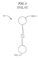
- FIG. 1 illustrates a network 10 that includes two computing devices 102-1,102-2.
- Network 10 is, for example, a wireless Bluetooth point-to-point piconet where wireless device 102-1 is a master Bluetooth system and wireless device 102-2 is a slave Bluetooth system, where the master 102-1 and slave 102-2 share the same channel.
- wireless device 102-1 is a master Bluetooth system
- wireless device 102-2 is a slave Bluetooth system, where the master 102-1 and slave 102-2 share the same channel.
- a point-to-point network need not include Bluetooth devices 102-1, 102-2 , but, rather, may comprise any type of computing device.
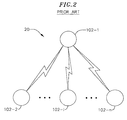
- FIG. 2 illustrates a network 20 that includes a plurality of wireless devices 102-1, 102-2 . 102-i ... 102-n (2 ⁇ i ⁇ n).
- Wireless network 20 is, for example, a point-to-multipoint Bluetooth piconet where wireless device 102-1 is a master Bluetooth system and wireless devices 102-2 through 102-n are slave Bluetooth systems. As with all piconets, the master 102-1 and all the slaves 102-2 through 102-n communicate over the same channel. In at least one embodiment, up to seven slaves can be active in the piconet 102 .
- the number of active slaves supported in a piconet depends on many variables and design considerations. Any of a number of slaves can be supported.
- a point-to-point network need not include Bluetooth devices 102-1, 102-2, but, rather, may comprise any type of computing device.
- a point-to-multipoint piconet 20 may include many additional slaves that can remain locked to the master 102-1 in a so-called "parked" state.
- parked slaves cannot be active on the piconet channel, but remain synchronized to the master.
- up to 256 parked slaves may remain locked to the master.
- the master 102-1 controls the channel access. This results in a need for the master 102-1 to switch control from one slave to another as it controls channel access within the piconet.
- the master 102-1 identifies each slave through a unique network address assigned to each slave. When a transfer of information between two slaves in a piconet 10,20 is desired, the master 102-1 coordinates transmission between two slaves.
- slave 102-2 could be a wireless personal digital assistant (“PDA”) device equipped with a Bluetooth system and slave 102-i could be a wireless cellular telephone equipped with a Bluetooth system.
- the master 102-1 can coordinate communications between the two slaves 102-2, 102-i over the piconet channel to exchange, for instance, phone number information. To do so, the master 102-1 must switch focus between the first slave 102-2 , commanding it to transmit phone number data to the master 102-1 , and the second slave 102-i, commanding it to receive phone number data from the master 102-1 ,
- This switch in focus referred to herein as a "context switch” requires the master to be able to store and access context information regarding each slave in relatively rapid succession.
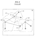
- Figure 3 illustrates that context-switching ability is also required for slaves that participate in more than one piconet.
- Figure 3 illustrates, for instance, a "scatternet" 30, formed from multiple networks with overlapping coverage,
- a Bluetooth piconet 31, 33, 20 ( Figure 2) can form part of a larger Bluetooth scatternet 30.
- Each piconet 31, 33, 20 ( Figure 2) can only have a single master 36, 34 and 102-1, respectively.
- Figure 3 illustrates that slaves can participate in multiple piconets on a time-division multiplex basis.
- slave 32 participates in two piconets: piconet 20 having master 102-1 and piconet 31 having master 36.
- a master 34 in one piconet 33 can be a slave in another piconet 37.
- a set of hardware registers is used to contain current context information.
- the information in the registers for outgoing context is stored from the registers to a memory location, such as a location in main memory or in a cache.
- the context information for the incoming context is then loaded from a different memory location into the registers.
- This storing to, and loading from, memory to transfer, via software, data between memory and hardware registers is time-consuming and processor-intensive.
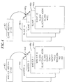
- FIG 4 is a generalized block diagram illustrating a context-switching register architecture according to at least one embodiment of the present invention.
- Computer systems such as the host computer 970 illustrated in Figure 9 , typically have a relatively large, relatively slow main memory.
- multiple dynamic random access memory (DRAM) modules comprise the main memory system.
- the time that it takes to transfer a set of bytes of information from the main memory to the microprocessor ("access time") of modern DRAMs is longer than the clock cycle length of modern microprocessors.
- a register is a storage location provided within the microprocessor or a peripheral device, where the storage location may be identified by an instruction as storing an operand.
- a register is "programmer visible"; the programmer may code an instruction that has the register as an operand identifier. Since registers are included within the microprocessor or peripheral, and because the register address is coded directly into an instruction, registers can be accessed rapidly.
- Figure 4 illustrates that the architecture scheme in accordance with at least one embodiment of the present invention includes a plurality of hardware registers 40, 42, 44a-44n, 46a-46m that maintain context information.
- the hardware registers 40, 42, 44a-44n, 46a-46m are provided in a peripheral system 972 ( Figure 9) rather than in the microprocessor of a host computer 970 ( Figure 9) .
- four master registers 44a-44n and four slave registers 46a-46n are provided.
- the architecture illustrated in Figure 4 also includes a master index 40 and a slave index register 42 , Because many devices can act as either masters or slaves, at least one embodiment of the present invention includes master registers 44a-44n and master index register 40, as well as slave registers 46a-46m and slave index register 42 in every network device operating in a master/slave environment.
- master registers 44a-44n and master index register 40 as well as slave registers 46a-46m and slave index register 42 in every network device operating in a master/slave environment.
- at least one embodiment of the present invention need only include the slave registers 46a-46m and the slave index register 42, but not the master registers 44a-44n or the master index register 40 , in devices that only act as masters.
- at least one embodiment of the present invention need include only the master registers 44a-44n and the master index register 40, but not the slave registers 46a-46m or the slave index register 42, in devices that only act as slaves.
- the present architecture is therefore scalable to accommodate any number of master registers 44a-44n and slave registers 46a-46m .
- a computing device acting as a master can maintain four slave registers 46a-46m
- the number of slave registers 46a-46m is, of course, scalable.
- a master 102-1 ( Figure 1), 36 ( Figure 3) can control up to seven slaves 102-2-102-n according to ver.
- At least one embodiment of the present invention includes seven slave registers 46a-46m in each Bluetooth system 102-1 ( Figure 1), 36 ( Figure 3) that is capable of acting as a master.
- a Bluetooth master system 102-1 ( Figure 1), 36 ( Figure 3) includes 256 slave registers 46a-46m in order to maintain context information for 256 parked slaves.
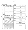
- Figure 5 and Table 1 set forth an exemplary format of the information stored in each slave register 46 .
- the format of the slave registers 46 will depend on specific design considerations. In general, the slave registers 46 contain any context information and parameters necessary to allow the master system 102-1 ( Figure 1), 36 ( Figure 3 ) to quickly switch contexts among slave systems.
- the format and the addresses of the information set forth in Figure 5 and Table 1 should be taken to be an exemplary format and address scheme only.
- the fields may be stored in any order, at any register location.
- Table 1 address name reset readable /writable bit location connection field description # of bits default 0xC1 NAP_hi s R/W [7:0] NAP[15:8] 0xc1 8 x00 NAP-lo s R/W [7:0] NAP [7:0] 0xc2 8 x00 UAP s R/W [7:0] UAP[7:0] 0xc3 8 x00 LAP_hi s R/W [7:0] LAP[23:16] 0xc4 8 x00 LAP_md s R/W [7:0] LAP[15:8] 0xc5 8 x00 LAP_lo s R/W [7:0] LAP[7:0] 0xc6 8 x00 0xC7 Class_hi s R/W [7:0] class[23:16] 0xc7 8 x00 Class_md s R/W [
- the NAP (Non-significant Address Part), UAP (Upper Address Part), and LAP (Lower Address Part) fields reflected in Table 1 together comprise the Bluetooth device network address (sometimes referred to herein as the "BD address") for the slave system being tracked in the particular register 46.
- the BD address is, in at least one embodiment, 48 bits long.
- the class fields (Class_hi, Class_md, Class_lo) reflected in Table 1 refer to the particular class of Bluetooth slave system being tracked in the particular register 46.
- PC computers, cellular phones, and personal digital assistants represent different classes of Bluetooth slave devices.
- the clock offset fields (clock offset upper, clock offset hi, clock offset md, clock offset lo) reflected in Table 1 represent a delta value between the master's clock and the slave's clock that the slave system maintains in order to synchronize its communications with the master system.
- This synchronization is required for the hopping scheme provided for in the Bluetooth Specification.
- the hopping scheme provides that the channel on which the Bluetooth systems in a piconet operate is represented by a pseudo-random hopping sequence through the available channels in the 2.4 GHz ISM band.
- the hopping sequence is unique for a piconet and is determined by the BD address of the master.
- the phase in the hopping sequence is determined by the Bluetooth clock of the master system. For this reason, the slave maintains the clock offset fields in order to hop in accordance with the master's clock.
- the AM_ADDR field represented in Table 1 is an active member address field containing the active slave's particular address within the piconet. It is used to distinguish among the active members of a piconet. For instance, a piconet that is capable of containing up to seven active slaves must provide for a unique piconet address for each of the active slaves.
- Table 1 illustrates that, in at least one embodiment, the AM_ADDR field is three bits long because three bits are needed to generate a binary representation of the number 7 (i.e., lb' 111').
- the FHS_misc field represented in Table 1 is a field containing the following sub-fields: scan repetition, scan period, and page scan mode. These fields relate to time periods, intervals, and mode for the paging procedure by which connections are established in Bluetooth piconets.
- a master device sends out a page message to a slave device with which the master is attempting to establish a connection.
- a slave that is not already connected periodically wakes up in a page scan state and looks for pages that may have been sent to it. In the page scan state, the slave scans for, and receives, page messages. When a page message is successfully received by the slave, there is a synchronization between the master and the slave, thereby establishing a connection between the master and the slave,
- Figure 6 and Table 2 set forth an exemplary format of the information stored in each master register 44.
- the format of the master registers 44 will depend on specific design considerations.
- the master registers 44 contain any context information and parameters necessary to allow the slave system 102-2-102-n ( Figure 2) to quickly switch contexts among master systems.
- the format and the addresses of the information set forth in Figure 6 and Table 2 should be taken to be an exemplary format and address scheme only.
- the fields may be stored in any order, at any register location.
- Table 2 address name reset readable / writable bit location connection field description # of bits default 0x82 NAP_hi s R/W [7:0] NAP[15:8] 0x82 8 x00 NAP-lo s R/W [7:0] NAP [7:0] 0x83 8 x00 UAP s R/W [7:0] UAP[7:0] 0x84 8 x00 LAP_hi s R/W [7:0] LAP[23:16] 0x85 8 x00 LAP_md s R/W [7:0] LAP[15:8] 0x86 8 x00 LAP_lo s R/W [7:0] LAP[7:0] 0x87 8 x00 0x88 Class_hi s R/W [7:0] class[23:16] 0x88 8 x00 Class_md s R/W [7:0] class[15:
- the NAP (Non-significant Address Part), UAP (Upper Address Part), and LAP (Lower Address Part) fields reflected in Table 2 together comprise the BD address for the master system being tracked in the particular register 44 .
- the BD address is, in at least one embodiment, 48 bits long.
- the class fields (Class_hi, Class_md, Class_lo) reflected in Table 2 refer to the particular class of Bluetooth master system being tracked in the particular register 44 .
- the master clock offset fields (clock offset upper, clock offset hi, clock offset md, clock offset lo) reflected in Table 2 represent a delta value between the slave's clock and the master's clock.
- the master can take this value into account when communicating with a slave in order to plan for a more efficient transmission.
- the AM_ADDR field represented in Table 2 is an active member address field containing the master's particular address within the piconet. It is used by the slave when addressing communication packets to the master.
- the AM_ADDR field in the master register 44 is a 3-bit field as explained above in connection with Table 1 .
- the FHS_misc field represented in Table 2 is a field containing the following sub-fields: scan repetition, scan period, and page scan mode, as is explained above in connection with Table 1.
- the PM_ADDR and AR_ADDR fields relate to the park mode. That is, even when a slave is parked, the slave maintains master context data in its master registers 44. When a slave device transitions from a park mode to a slave mode, the slave gives up its AM_ADDR active member address value. Instead, the parked slave receives two new addresses, assigned by the master, to be used in the park mode: PM_ADDR (parked member address) and AR_ADDR (access request address). PM_ADDR distinguishes a parked slave from other parked slaves. In tracking context data for one or more masters, the parked slave keeps track of its PM_ADDR for each master- the PM_ADDR is used by the master in a master-initiated unpark procedure. The AR_ADDR is a master-assigned address to be used by the slave in a slave-initiated unpark procedure.
- the next several fields depicted in Table 2 relate to a "sniff" mode. These fields include the Dsniff fields (Dsniff_hi, Dsniff_lo), the Tsniff fields (Tsniff_hi, Tsniff_lo), the Nsniff attempt fields (Nsniff attempt hi, Nsniff attempt lo), and the Nsniff timeout fields (N sniff timeout hi, N sniff timeout lo).
- the sniff mode the duty cycle of an active slave's listen activity is reduced because the time slots in which the master can start transmission to a specific slave are reduced to specified time slots. Therefore, when an active slave is in sniff mode, it need only listen during its assigned sniff slots.
- sniff slots are spaced regularly within an interval of Tsniff .
- the slave must listen at the Dsniff slot every sniff period, Tsniff , for an N sniff attempt number of times. If the slave receives a packet during its sniff period, it should continue listening as long as it continues to receive packets. Once the slave stops receiving packets, it should continue listening for Nsniff timeout more slots or the remaining of the N sniff attempt number of slots, whichever is greater.
- the hold timeout fields (holdTO_hi, holdTO_lo)relate to a hold mode.
- a slave can be put into a hold mode wherein the slave is still active but its communication abilities on the channel are temporarily limited.
- the slave keeps its active member address (AM_ADDR).
- A_ADDR active member address
- the slave and master agree on the time duration that the slave is to remain in the hold mode. This time value is stored in the hold timeout fields.
- the remaining fields represented in Table 2 relate to the beacon channel.
- the master establishes a beacon channel when one or more slaves are parked.
- the beacon channel is used for the transmission from the master to the parked slave of information that the slave can use for re-synchronization.
- the beacon channel is also used to carry messages to the parked slaves to change the beacon parameters and to carry general broadcast messages to the parked slaves.
- the beacon channel is used for the unparking of one or more parked slaves.
- Figure 9 illustrates the organization of at least one embodiment of a Bluetooth system 900, which is relevant to the following discussion.
- a Bluetooth system 900 such as a cell phone or a PDA, consists of a host computer 970 and a peripheral system 972 .
- the peripheral system 972 includes an analog component and a digital component.
- the analog component is a radio unit 910 .
- radio unit 910 For additional details concerning the operation of at least one aspect of at least one other embodiment of the radio unit 910 , please refer to co-pending application U.S. Pat, App. No.09/592,016, Attorney Docket Number M-8891 US, by inventor Albert Liu, entitled “Receiver Architecture Employing Low Intermediate Frequency And Complex Filtering", filed June 12, 2000, which is herein incorporated by reference in its entirety for all purposes.
- the digital component of the peripheral system 972 is the host controller 930 .
- a computing device such as those 102-1,102-2 through 102-n depicted in Figures 1 and 2 need not necessarily contain all of the elements depicted in Figure 9 in order to practice the present invention.
- the host controller 930 includes hardware components (circuitry) 920, 940, 950 and software components 960, 980 .
- the external interface 950 performs link management and provides interface functions with a host computer 970.
- the host 970 communicates with the host controller 930 via the software of the host interface 980 as it operates on the external interface hardware 950.
- the host 970 receives asynchronous event notifications when a significant event has occurred.
- the host 970 parses the notification to determine what event has occurred.
- Part H:1, "Host Controller Interface Functional Specification" of ver. 1.0b of the Bluetooth Specification which is hereby incorporated by reference or all purposes.
- the link controller 920 performs Bluetooth baseband processing and handles physical layer protocols.
- the Link Manager software 960 discovers other remote link manager programs and utilizes the services of the link controller 920 to communicate with them.
- Figure 9 illustrates that the Link Manager software 960 runs on the state machine 940.
- the state machine 940 provides hardware circuits that provide access to the register architecture discussed above in connection with Figure 4.
- Figures 7, 8 and 9 illustrate that the state machine 940 includes a control portion 944, a data portion 946, and an address portion 942.
- the data portion of the state machine 940 includes the master registers 44a-44n , the master index register 40, the slave registers 46a-46m , and the slave index register 42.
- the address portion 942 of the state machine 940 includes circuits referred to as the Corereg circuit 970 and the Regmux circuit 972.
- Figure 7 is a block diagram depicting the use of the master index to perform context-switching for a slave device.
- Figure 7 illustrates that the contents of the master index register 40 are used to select which of the master registers 44 the slave wishes to access. For instance, if the slave wishes to access a first master register 44a, then a value of 1 b'00000000' is loaded by the host 970 into the master index register 40 . For each of the remaining master registers 44b-44n, a corresponding index value is loaded into the master index register 40 when the slave needs to retrieve context data stored in that particular master register 44b-44n.
- the Corereg circuit 70 and Regmux circuit 72 perform logic, described below, to read from, or write to, the master register 44 of interest.
- a context switch when a slave desires to switch contexts among masters, is thus performed simply by the host computer's 970 changing of the value in the master index register 40.
- Figure 8 is a block diagram depicting the use of the slave index to perform context-switching for a master device.
- Figure 8 illustrates that the contents of the slave index register 42 are used to select which of the slave registers 46 the master wishes to access. For instance, if the master wishes to access a third master register 46c, then a value of 1b'00000011' is loaded into the slave index register 42. For each of the remaining slave registers, a corresponding index value is loaded into the slave index register 42 when the master wishes to retrieve context data stored in that particular master register.
- FIGs 8 and 9 illustrate that, once the host computer 970 loads the slave index register 42 with the appropriate value, then the Corereg circuit 70 and Regmux circuit 72 perform logic, described below, to read from, or write to, the slave register 46 of interest.
- a context switch when a master desires to switch contexts among slaves, is thus performed simply by the host computer's 970 changing of the value in the slave index register 42 so that the Corereg 70 and Regmux 72 circuits can operate to retrieve and/or modify the specified contents of the slave register 46 of interest.
- FIG. 7 illustrates that a slave system having a master index 40 and one or more master registers 44 can quickly perform context-switching among masters. Because the information described above in Table 1 is stored in the slave registers 46, and the information described above in Table 2 is stored in the master registers 44, the context information need not be stored in software data structures nor stored on the microprocessor of the host computer 970 . This allows the context data to be accessed more quickly than if it were transferred from memory to registers upon a context switch.
- While software running on the host computer 970 does not need to store the context information, it still needs to be able to identify and access the particular context data for the incoming slave that a master is interested in switching to, and must be able to identify and access the particular context data for the incoming master that a slave is interested in switching to.
- This function of identifying and accessing the context information for the incoming slave or master is accomplished through the use of a slave index 42 and master index 40, respectively.
- the slave index 42 is located at register memory location 0xC0 and the master index 40 is located at register memory location 0x81.
- Pickett '646 provides within a microprocessor an expanded set of registers in addition to the architected set of registers.
- the present architecture does not require that the context information be moved from registers (architected or otherwise) in the host computer 970 to the peripheral system 972 each time a context switch occurs. Such transfer slows down the context-switch operation and burdens the network with transmission of context information.
- the present architecture therefore provides for versatility in network systems by permitting the use of slower, lower performance host computers 970 while still supporting relatively fast context switches.
- Figure 7, Figure 8, and Figure 9 illustrate that the Corereg circuit 700 is a logic circuit included in the address portion 942 of the state machine 940 .
- the Corereg circuit 700 performs logic to access the desired location within a master register 44 or slave register 46.
- At least one embodiment of the Corereg register access circuit 70 may be implemented, for example, by Verilog source code listed in Appendix A.
- the Corereg register access circuit 70 receives various input values that are provided by software running on the host system 970.
- One such input value is an Addr_ in value, which represents the particular address of the desired field within the master register 44 or slave register 46 of interest.
- Another input value is the index value in either the master index register 40 or the slave index register 42 .
- a slave system 32 may switch contexts from a first master 102-1 (whose context information is tracked, say, in master register 44a ) to a second master 36 (whose context information is tracked, say, in master register 44b ).
- an index value of 4b'0000' represents the first master register 44a while an index value of 4b'0001' represents the second master register 44b .
- link controller 920 ( Figure 9) replaces the index value of 4b'000' with an index value of4b'0001' in the master index register 40. In this manner, a context switch has occurred.
- the Addr_in input address is the address of the particular field within a slave register 46 or master register 44.
- Table 1 indicates that the link controller 920 ( Figure 9) would set Addr_in to a value of 4b'0xCE' if a master needed to read or modify the AM_ADDR field for a particular active slave.
- Figure 7 and Figure 8 illustrate that the Corereg module 70 includes logic provided by the Regmux 72 circuit.
- the Regmux circuit 72 is a circuit defined by the Verilog source code listed in Appendix B and is a mux circuit that, given the proper index value and Addr_in value, returns the specific register location of interest.
- Corereg 70 and Regmux 72 circuits may be performed by hardware modules, or may be implemented as software modules, firmware modules, or any combination thereof.
- processing may be implemented as a single hardware or software module that includes various logical functions, rather than separate modules. If implemented in software modules, the software can be executed, for instance, by an embedded CPU that is used instead of the state machine 940 .
- FIG 11 is a flowchart illustrating a master parameter access software module 1100 that invokes the logic of the state machine 940 to access information in a master register 44.
- the master parameter access module 1100 contains machine-executable instructions that are executed, for example, on the host computer 970.
- Figure 11 illustrates that the host 970 , when executing operation 1102, loads the appropriate index value into the master index register 40. For instance, if the master register of interest 44 is a second master register (where the index value for a first master register is zero), then a value of 4b'01' is loaded by the host 970 into the master index register 40 in operation 1102. The host computer 970 then executes operation 1104. Operation 1104 invokes the Corereg logic circuit 70 ( Figure 7) to write or read from the register of interest 44. Operation 1104 includes a read path and a write path.
- Figures 9 and 11 illustrate that, during the read path of operation 1104, the host computer 970 provides the following inputs and then invokes the Corereg logic circuit 70 :
- the host computer 970 provides the following inputs and then invokes the logic of the Corereg logic circuit 70:
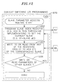
- FIG 12 is a flowchart illustrating a slave parameter access software module 1200 that invokes the logic of the state machine 940 to access information in a slave register 46 .
- the slave parameter access module 1200 contains machine-executable instructions that are executed, for example, on the host computer 970 .
- Figure 12 illustrates that the host computer 970, when executing operation 1202, loads the appropriate index value into the slave index register 42. For instance, if the slave register of interest 46 is a second slave register (where the index value for a first slave register is zero), then a value of 4b'01' is loaded by the host 970 into the slave index register 42 in operation 1202 . The host computer 970 then executes operation 1204. Operation 1204 invokes the Corereg logic circuit 70 ( Figure 7) to write or read from the register of interest 46. Operation 1204 includes a read path and a write path.
- FIGS 9 and 12 illustrate that, during the read path of operation 1204, the host computer 970 provides the following inputs and then invokes the Corereg logic circuit 70:
- the host computer 970 provides the following inputs and then invokes the logic of the Corereg logic circuit 70:
- the master parameter access module 1100 and the slave parameter access module 1200 have been described as a series of sequential operations, the operations need not necessarily be performed in the order discussed. Instead, the operations may be performed in any order that preserves the functionality described herein. For instance, the respective inputs of the read and write paths may be provided in any order in operations 1104 and 1204 .
- operations that have been shown as separate operations may be performed in the same logical group on instructions.
- the computer-readable instructions included in the present invention can be implemented as software instructions on a computer-readable tangible medium such as any magnetic storage medium, including disk and tape storage medium; an optical storage medium, including compact disk memory and a digital video disk storage medium; a nonvolatile memory storage memory; a volatile storage medium; or data transmission medium including packets of electronic data and electromagnetic waves modulated in accordance with the instructions.
- a computer-readable tangible medium such as any magnetic storage medium, including disk and tape storage medium; an optical storage medium, including compact disk memory and a digital video disk storage medium; a nonvolatile memory storage memory; a volatile storage medium; or data transmission medium including packets of electronic data and electromagnetic waves modulated in accordance with the instructions.
- the context-switching architecture disclosed herein may be used in any network environment where context-switching among computing devices is performed.
- the present invention may be employed in any network, such as a client/server network, and need not necessarily be employed in a master/slave network environment.
- the registers described herein need not contain master and slave data, but can rather contain any context data.
Landscapes
- Engineering & Computer Science (AREA)
- Software Systems (AREA)
- Theoretical Computer Science (AREA)
- Physics & Mathematics (AREA)
- General Engineering & Computer Science (AREA)
- General Physics & Mathematics (AREA)
- Mobile Radio Communication Systems (AREA)
- Executing Machine-Instructions (AREA)
- Small-Scale Networks (AREA)
Abstract
Description
- Portions of this patent application contain materials that are subject to copyright protection. The copyright owner has no objection to the facsimile reproduction by anyone of the patent document, or the patent disclosure, as it appears in the Patent and Trademark Office file or records, but otherwise reserves all copyright rights whatsoever.
- This invention relates to computing systems and, more particularly, to an architecture and system for switching contexts, where the context switching is accelerated through the use of hardware registers to store context data.
- The Bluetooth Specification is an open technical specification and a de facto standard for a wireless (radio) communication technology. The Bluetooth technology is a short-range low-power radio link for transmission of digital data and analog voice data. Bluetooth allows the replacement of the numerous and varied proprietary cables that connect one computer or communication device to another with one universal short-range radio link. Users can therefore connect a wide range of computing and telecommunications devices without the need to buy, carry, or connect cables. For example, a computer can communicate with a printer via a radio link instead of a cable. Bluetooth also allows computing devices to connect to a communicating device via a radio link. For example, a computer can communicate with a cell phone via a radio link to access the Internet.
- Bluetooth systems connect to each other in piconets, which are formed by a master system connecting with at least one other system sharing the same channel. Most Bluetooth systems can act as either a master or a slave; the terms "master" and "slave" merely refer to the roles played by each device within a particular piconet. One Bluetooth system acts as the master of the piconct. In addition to the master, a piconet may include an additional number of Bluetooth systems that act as slaves. For more details, please refer to "Specification of the Bluetooth System-Core v1.0b" available from the Bluetooth Special Interest Group at its web site. Part B, "Baseband Specification", of Vol. I("Core") ver. 1.0b of the Bluetooth Specification is herein incorporated by reference in its entirety for all purposes.
- Each master of a Bluetooth piconet can switch contexts from one slave to another. In addition, because a slave can participate in more than one piconet, a slave can switch contests among masters. Traditional approaches render the context-switch process slow and cumbersome. What is needed is a system and method for performing relatively rapid context switches while still retaining an acceptable level of network throughput.
- A method of performing a context switch operation involves accessing context data in a first register of a peripheral system, where the first register is associated with a first index register. The method further includes receiving a second index value from a host computer associated with the peripheral system. The host computer's providing of the second index value when the peripheral system had been accessing the first register causes a context switch from the first register to the second register. Accordingly, the method further includes accessing context data in a second register of the peripheral system, where the second register is associated with the second index value. In at least one embodiment of the method, the first and second registers are not architected registers.
- In at least one embodiment, accessing the context data in the second register further comprises performing a write function to an identified address within the second register. In at least one other embodiment, accessing the context data in the second register further comprises providing the contents of an identified address within the second register to the host computer. In at least one other embodiment, accessing the context data in the second register further comprises performing a read operation, depending on the value of a control input. In at least one other embodiment, accessing the context data in the second register further comprises performing a write operation, depending on the value of a control input.
- At least one embodiment of a system comprises a host computer that includes a microprocessor, at least one peripheral system coupled to the host computer, an interface between the host computer and the peripheral system, and a register access circuit coupled to the peripheral system. The peripheral system includes a first register that is associated with a first index value and also includes a second register that is associated with a second index value. The interface is configured to provide the first and second index values from the host computer to the peripheral system. The register access circuit is configured to access data in the first register if the first index value is provided by the host computer and is further configured to access data in the second register if the second index value is provided by the host computer. In at least one embodiment of the system, the first and second registers are not architected registers.
- At least one embodiment of the peripheral system further includes a state machine, where the state machine includes an address portion, a control portion, and a data portion, where the first and second registers are included in the data portion. At least one embodiment of the address portion includes a register access circuit. At least one other embodiment of the peripheral system further includes a microprocessor. At least one other embodiment of the peripheral system includes at least one index register. At least one other embodiment of the peripheral system includes a plurality of context registers, with each of the plurality of context registers being associated with one of a plurality of index values.
-
- FIG. 1 illustrates, in a block diagram, a point-to-point network between two computing devices.
- FIG. 2 illustrates, in a block diagram, a point-to-multipoint network among a plurality of computing devices.
- FIG. 3 is a block diagram illustrating a scatternet that includes multiple piconets with overlapping coverage.
- FIG. 4 is a block diagram illustrating a register architecture for maintaining master and slave context information in a peripheral device.
- FIG. 5 is a block diagram illustrating at least one embodiment of the format of a slave index and slave register.
- FIG. 6 is a block diagram illustrating at least one embodiment of the format of a master index and master register.
- FIG. 7 is a data flow diagram illustrating at least one embodiment of the data flow during the use of a master index to perform context-switching for a slave device.
- FIG. 8 illustrates a data flow diagram illustrating at least one embodiment of the data flow during the use of a slave index to perform context-switching for a master device.
- FIG. 9 illustrates at least one embodiment of a system embodying the context-switch architecture of the present invention.
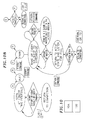
- FIG. 10, including FIG. 10a and FIG. 10b, is a state transition diagram illustrating a state machine according to one embodiment of the present invention.
- FIG. 11 is a flowchart illustrating at least one embodiment of a master parameter access module.
- FIG. 12 is a flowchart illustrating at least one embodiment of a slave parameter access module.
- Figure 1 illustrates a
network 10 that includes two computing devices 102-1,102-2. Network 10 is, for example, a wireless Bluetooth point-to-point piconet where wireless device 102-1 is a master Bluetooth system and wireless device 102-2 is a slave Bluetooth system, where the master 102-1 and slave 102-2 share the same channel. One skilled in the art will recognize that a point-to-point network need not include Bluetooth devices 102-1, 102-2, but, rather, may comprise any type of computing device. - Figure 2 illustrates a
network 20 that includes a plurality of wireless devices 102-1, 102-2. 102-i... 102-n (2 ≤ i ≤ n).Wireless network 20 is, for example, a point-to-multipoint Bluetooth piconet where wireless device 102-1 is a master Bluetooth system and wireless devices 102-2 through 102-n are slave Bluetooth systems. As with all piconets, the master 102-1 and all the slaves 102-2 through 102-n communicate over the same channel. In at least one embodiment, up to seven slaves can be active in thepiconet 102. One skilled in the art will recognize that the number of active slaves supported in a piconet depends on many variables and design considerations. Any of a number of slaves can be supported. One skilled in the art will further recognize that a point-to-point network need not include Bluetooth devices 102-1, 102-2, but, rather, may comprise any type of computing device. - In addition to the active slaves 102-2, 102-i through 102-n illustrated in Figure 2, a point-to-
multipoint piconet 20 may include many additional slaves that can remain locked to the master 102-1 in a so-called "parked" state. When a slave does not need to participate on the piconet channel, but still needs to remain synchronized to the channel it can enter the low-power parked state. These parked slaves cannot be active on the piconet channel, but remain synchronized to the master. In at least one embodiment, up to 256 parked slaves may remain locked to the master. For additional information regarding an implementation of the synchronization of master and slave Bluetooth systems, please refer to the commonly assigned application bearing U.S. Patent Application Serial No. 09/593,583, entitled "Wireless Data Communications Using FIFO For Synchronization Memory," by inventors Sherman Lee, Vivian Y. Chou, and John H. Lin, filed June 12, 2000, attorney docket number M-8741 US, which is herein incorporated by reference for all purposes. - For both active and parked slaves in a
single piconet piconet - Referring to Figure 2, for instance, slave 102-2 could be a wireless personal digital assistant ("PDA") device equipped with a Bluetooth system and slave 102-i could be a wireless cellular telephone equipped with a Bluetooth system. In such case, the master 102-1 can coordinate communications between the two slaves 102-2, 102-i over the piconet channel to exchange, for instance, phone number information. To do so, the master 102-1 must switch focus between the first slave 102-2, commanding it to transmit phone number data to the master 102-1, and the second slave 102-i, commanding it to receive phone number data from the master 102-1, This switch in focus, referred to herein as a "context switch" requires the master to be able to store and access context information regarding each slave in relatively rapid succession.
- Figure 3 illustrates that context-switching ability is also required for slaves that participate in more than one piconet. Figure 3, illustrates, for instance, a "scatternet" 30, formed from multiple networks with overlapping coverage, A
Bluetooth piconet larger Bluetooth scatternet 30. Eachpiconet single master slave 32 participates in two piconets:piconet 20 having master 102-1 andpiconet 31 havingmaster 36. In addition, amaster 34 in onepiconet 33 can be a slave in another piconet 37. - The discussion above illustrates the need, in a network environment such as, for instance, a wireless network as specified in the Bluetooth Specification, for both masters and slaves to have the ability to quickly switch contexts in order to facilitate orderly, reasonably rapid communication among wireless devices. In a different context, several schemes exist for switching contents among software application programs. These schemes usually involve storing context information in memory and then, during a context switch, loading the information from memory into a particular register or set of registers. Such software-based context-switching schemes are disclosed, for example, in U.S. Pat. No. 6,061,711, entitled "Efficient Context Saving and Restoring in a Multi-Tasking Computing System Environment", and issued to Song et al. and also in U.S. Pat. No. 5,812,823, entitled "Method and System for Performing an Emulation Context Save and Restore That is Transparent to the Operating System", and issued to Kahle et al. Song '711 and Kahle '823 are hereby incorporated by reference for all purposes.
- In a software-based context-switching scheme, a set of hardware registers is used to contain current context information. When a context switch occurs, the information in the registers for outgoing context is stored from the registers to a memory location, such as a location in main memory or in a cache. The context information for the incoming context is then loaded from a different memory location into the registers. This storing to, and loading from, memory to transfer, via software, data between memory and hardware registers is time-consuming and processor-intensive. To employ such an approach for switching contexts among masters and slaves in a network of computing devices, such as a network of Bluetooth systems, would result severely limited network throughput during the context-switch process.
- Figure 4 is a generalized block diagram illustrating a context-switching register architecture according to at least one embodiment of the present invention. A preliminary discussion of general register architectures is appropriate before discussing the particular aspects of the register architecture of the present invention. Computer systems, such as the
host computer 970 illustrated in Figure 9, typically have a relatively large, relatively slow main memory. Typically, multiple dynamic random access memory (DRAM) modules comprise the main memory system. The time that it takes to transfer a set of bytes of information from the main memory to the microprocessor ("access time") of modern DRAMs is longer than the clock cycle length of modern microprocessors. - In order to provide a faster means for the microprocessor to access stored information, a set of registers is usually provided within the microprocessor. As used herein, a register is a storage location provided within the microprocessor or a peripheral device, where the storage location may be identified by an instruction as storing an operand. In other words, a register is "programmer visible"; the programmer may code an instruction that has the register as an operand identifier. Since registers are included within the microprocessor or peripheral, and because the register address is coded directly into an instruction, registers can be accessed rapidly.
- Figure 4 illustrates that the architecture scheme in accordance with at least one embodiment of the present invention includes a plurality of hardware registers 40, 42, 44a-44n, 46a-46m that maintain context information. In at least one embodiment, the hardware registers 40, 42, 44a-44n, 46a-46m are provided in a peripheral system 972 (Figure 9) rather than in the microprocessor of a host computer 970 (Figure 9). In at least one embodiment, n=8 and m=8, such that eight
master registers 44a-44n and eightslave registers 46a-46m are provided. In at least one other embodiment, which is illustrated in Figure 4, fourmaster registers 44a-44n and fourslave registers 46a-46n are provided. The architecture illustrated in Figure 4 also includes amaster index 40 and aslave index register 42, Because many devices can act as either masters or slaves, at least one embodiment of the present invention includes master registers 44a-44n andmaster index register 40, as well as slave registers 46a-46m andslave index register 42 in every network device operating in a master/slave environment. One skilled in the art will recognize that at least one embodiment of the present invention need only include the slave registers 46a-46m and theslave index register 42, but not the master registers 44a-44n or themaster index register 40, in devices that only act as masters. Similarly, at least one embodiment of the present invention need include only the master registers 44a-44n and themaster index register 40, but not the slave registers 46a-46m or theslave index register 42, in devices that only act as slaves. - One skilled in the art will further recognize that numerous design considerations affect the number, size and organization of the master registers 442-44n and
slave registers 46a-46m. The present architecture is therefore scalable to accommodate any number of master registers 44a-44n andslave registers 46a-46m. For instance, while a computing device acting as a master can maintain fourslave registers 46a-46m, the number of slave registers 46a-46m is, of course, scalable. For example, because a master 102-1 (Figure 1), 36 (Figure 3) can control up to seven slaves 102-2-102-n according to ver. 1.0b of the Bluetooth Specification, at least one embodiment of the present invention includes sevenslave registers 46a-46m in each Bluetooth system 102-1 (Figure 1), 36 (Figure 3) that is capable of acting as a master. In at least one other embodiment, a Bluetooth master system 102-1 (Figure 1), 36 (Figure 3) includes 256slave registers 46a-46m in order to maintain context information for 256 parked slaves. - Figure 5 and Table 1 set forth an exemplary format of the information stored in each
slave register 46. One skilled in the art will recognize that the format of the slave registers 46 will depend on specific design considerations. In general, the slave registers 46 contain any context information and parameters necessary to allow the master system 102-1 (Figure 1), 36 (Figure 3) to quickly switch contexts among slave systems. The format and the addresses of the information set forth in Figure 5 and Table 1 should be taken to be an exemplary format and address scheme only. One skilled in the art will recognize that the fields may be stored in any order, at any register location.Table 1 address name reset readable /writable bit location connection field description # of bits default 0xC1 NAP_hi s R/W [7:0] NAP[15:8] 0xc1 8 x00 NAP-lo s R/W [7:0] NAP [7:0] 0xc2 8 x00 UAP s R/W [7:0] UAP[7:0] 0xc3 8 x00 LAP_hi s R/W [7:0] LAP[23:16] 0xc4 8 x00 LAP_md s R/W [7:0] LAP[15:8] 0xc5 8 x00 LAP_lo s R/W [7:0] LAP[7:0] 0xc6 8 x00 0xC7 Class_hi s R/W [7:0] class[23:16] 0xc7 8 x00 Class_md s R/W [7:0] class[15:8] 0xc8 8 x00 Class_lo s R/W [7:0] class[7:0] 0xc9 8 x00 0xCA clock offset upper s R/W [7:0] clock[27:24] 0xca 8 x00 clock offset hi s R/W [7:0] clock[23:16] 0xcb 8 x00 clock offset md s R/W [7:0] clock[15:8] 0xcc 8 x00 clock offset lo s R/W [7:6] clock[7:0] 0xcd 2 0 0xCE AM_ADDR s R/W [2:0] AM_ADDR 0xce 3 0 0xCF FHS_misc s R/W [7:6] Scan Repetition 0xcf 2 0 s R/W [5:4] Scan Period 2 0 s R/W [3:1] Page Scan Mode 3 0 - The NAP (Non-significant Address Part), UAP (Upper Address Part), and LAP (Lower Address Part) fields reflected in Table 1 together comprise the Bluetooth device network address (sometimes referred to herein as the "BD address") for the slave system being tracked in the
particular register 46. The BD address is, in at least one embodiment, 48 bits long. - The class fields (Class_hi, Class_md, Class_lo) reflected in Table 1 refer to the particular class of Bluetooth slave system being tracked in the
particular register 46. For instance, PC computers, cellular phones, and personal digital assistants represent different classes of Bluetooth slave devices. - The clock offset fields (clock offset upper, clock offset hi, clock offset md, clock offset lo) reflected in Table 1 represent a delta value between the master's clock and the slave's clock that the slave system maintains in order to synchronize its communications with the master system. This synchronization is required for the hopping scheme provided for in the Bluetooth Specification. The hopping scheme provides that the channel on which the Bluetooth systems in a piconet operate is represented by a pseudo-random hopping sequence through the available channels in the 2.4 GHz ISM band. The hopping sequence is unique for a piconet and is determined by the BD address of the master. The phase in the hopping sequence is determined by the Bluetooth clock of the master system. For this reason, the slave maintains the clock offset fields in order to hop in accordance with the master's clock.
- The AM_ADDR field represented in Table 1 is an active member address field containing the active slave's particular address within the piconet. It is used to distinguish among the active members of a piconet. For instance, a piconet that is capable of containing up to seven active slaves must provide for a unique piconet address for each of the active slaves. Table 1 illustrates that, in at least one embodiment, the AM_ADDR field is three bits long because three bits are needed to generate a binary representation of the number 7 (i.e., lb' 111').
- The FHS_misc field represented in Table 1 is a field containing the following sub-fields: scan repetition, scan period, and page scan mode. These fields relate to time periods, intervals, and mode for the paging procedure by which connections are established in Bluetooth piconets.
- A master device sends out a page message to a slave device with which the master is attempting to establish a connection. A slave that is not already connected periodically wakes up in a page scan state and looks for pages that may have been sent to it. In the page scan state, the slave scans for, and receives, page messages. When a page message is successfully received by the slave, there is a synchronization between the master and the slave, thereby establishing a connection between the master and the slave,
- Figure 6 and Table 2, below, set forth an exemplary format of the information stored in each
master register 44. One skilled in the art will recognize that the format of the master registers 44 will depend on specific design considerations. In general, the master registers 44 contain any context information and parameters necessary to allow the slave system 102-2-102-n (Figure 2) to quickly switch contexts among master systems. The format and the addresses of the information set forth in Figure 6 and Table 2 should be taken to be an exemplary format and address scheme only. One skilled in the art will recognize that the fields may be stored in any order, at any register location.Table 2 address name reset readable /writable bit location connection field description # of bits default 0x82 NAP_hi s R/W [7:0] NAP[15:8] 0x82 8 x00 NAP-lo s R/W [7:0] NAP [7:0] 0x83 8 x00 UAP s R/W [7:0] UAP[7:0] 0x84 8 x00 LAP_hi s R/W [7:0] LAP[23:16] 0x85 8 x00 LAP_md s R/W [7:0] LAP[15:8] 0x86 8 x00 LAP_lo s R/W [7:0] LAP[7:0] 0x87 8 x00 0x88 Class_hi s R/W [7:0] class[23:16] 0x88 8 x00 Class_md s R/W [7:0] class[15:8] 0x89 8 x00 Class_lo s R/W [7:0] class[7:0] 0x8a 8 x00 0x8B clock offset upper s R/W [7:0] clock[27:24] 0x8b 8 x00 clock offset hi s R/W [7:0] clock[23:16] 0x8c 8 x00 clock offset md s [7:0] clock[15:8] 0x8d 8 x00 clock offset lo s R/W [7:6] clock[7:0] Ox8e 2 0 0x8F AM_ADD R s R/W [2:0] AM_ADDR 0x8f 3 0 0x90 FHS_misc s R/W [7:6] Scan Repetition 0x90 2 0 R/W [5:4] Scan Period 2 0 R/W [3:1] Page Scan Mode 3 0 0x91 PM_ADDR s R/W [2:0] assigned PM_ADDR by master 0x91 8 0 0x92 AR_ADDR s R/W [2:0] assigned AR_ADDR by master 0x92 8 0 0x93 Dsniff_hi s R/W [7:0] connection specific Dsniff 0x93 8 x00 Dsniff_lo s R/W [7:0] 0x94 S x00 0x95 Tsniff_hi s R/W [7:0] Tsniff 0x95. 8 x00 Tsniff_lo s R/W [7:0] 0x96 8 x00 0x97 N sniff attempt hi s R/W [7:0] N sniff attempt 0 x97 8 x00 N sniff attempt lo s R/W [7:0] 0x98 8 x00 0x99 N sniff timeout hi s R/W [7:0] N sniff timeout 0x99 8 x00 N sniff timeout lo s R/W [7:0] 0x9a 8 x00 0x9B holdTO_hi s R/W [7:0] holdTO 0x9b 8 x00 holdTO_lo s R/W [7:0] 0x9c 8 x00 0x9D Tbeacon_hi s R/W [7:0] Park Beacon interval 0x9d 8 x00 0x9D Tbeacon_lo s R/W [7:0] 0x9e 8 x00 0x9F NB_hi s R/W [7:0] NB 0x9f 8 x00 NB_lo s R/W [7:0] 0xa0 8 x00 0xA1 DB_hi s RIW [7:0] DB 0xa1 8 x00 DB_lo s R/W [7:0] 0xa2 8 x00 0xA3 TB_hi s R/W [7:0] TB 0xa3 8 x00 TB_lo s R/W [7:0] 0xa4 8 x00 0xA5 Maccess_hi s R/W [7:0] Maccess 0xa5 8 x00 Maccess_lo s R/W [7:0] 0xa6 8 x00 0xA7 Taccess_hi s R/W [7:0] Taccess 0xa7 8 x00 Taccess_lo s R/W [7:0] 0xa8 8 x00 0xA9 Daccess_hi s R/W [7:0] Daccess 0xa9 8 x00 Daccess_lo s R/W [7:0] 0xaa 8 x00 0xAB Nacc_slot hi s R/W [7:0] Nacc_slot Oxab 8 x00 Nacc_slot lo s R/W [7:0] 0xac 8 x00 0xAD NB_sleep hi s R/W [7:0] NB_sleep 0xad 8 x00 NB_sleep lo s R/W [7:0] 0xae 8 x00 0xAF DB_sleep hi s R/W [7:0] DB_sleep 0xaf 8 x00 DB_sleep lo s R/W [7:0] 0xb0 8 x00 0xB1 Npoll hi s R/W [7:0] Npoll 0xb1 8 x00 Npoll lo s R/W [7:0] 0xb2 8 x00 - The NAP (Non-significant Address Part), UAP (Upper Address Part), and LAP (Lower Address Part) fields reflected in Table 2 together comprise the BD address for the master system being tracked in the
particular register 44. The BD address is, in at least one embodiment, 48 bits long. - The class fields (Class_hi, Class_md, Class_lo) reflected in Table 2 refer to the particular class of Bluetooth master system being tracked in the
particular register 44. - The master clock offset fields (clock offset upper, clock offset hi, clock offset md, clock offset lo) reflected in Table 2 represent a delta value between the slave's clock and the master's clock. The master can take this value into account when communicating with a slave in order to plan for a more efficient transmission.
- The AM_ADDR field represented in Table 2 is an active member address field containing the master's particular address within the piconet. It is used by the slave when addressing communication packets to the master. The AM_ADDR field in the
master register 44 is a 3-bit field as explained above in connection with Table 1. - The FHS_misc field represented in Table 2 is a field containing the following sub-fields: scan repetition, scan period, and page scan mode, as is explained above in connection with Table 1.
- The PM_ADDR and AR_ADDR fields relate to the park mode. That is, even when a slave is parked, the slave maintains master context data in its master registers 44. When a slave device transitions from a park mode to a slave mode, the slave gives up its AM_ADDR active member address value. Instead, the parked slave receives two new addresses, assigned by the master, to be used in the park mode: PM_ADDR (parked member address) and AR_ADDR (access request address). PM_ADDR distinguishes a parked slave from other parked slaves. In tracking context data for one or more masters, the parked slave keeps track of its PM_ADDR for each master- the PM_ADDR is used by the master in a master-initiated unpark procedure. The AR_ADDR is a master-assigned address to be used by the slave in a slave-initiated unpark procedure.
- The next several fields depicted in Table 2 relate to a "sniff" mode. These fields include the Dsniff fields (Dsniff_hi, Dsniff_lo), the Tsniff fields (Tsniff_hi, Tsniff_lo), the Nsniff attempt fields (Nsniff attempt hi, Nsniff attempt lo), and the Nsniff timeout fields (N sniff timeout hi, N sniff timeout lo). In the sniff mode, the duty cycle of an active slave's listen activity is reduced because the time slots in which the master can start transmission to a specific slave are reduced to specified time slots. Therefore, when an active slave is in sniff mode, it need only listen during its assigned sniff slots. These so-called sniff slots are spaced regularly within an interval of Tsniff. The slave must listen at the Dsniff slot every sniff period, Tsniff, for an N sniff attempt number of times. If the slave receives a packet during its sniff period, it should continue listening as long as it continues to receive packets. Once the slave stops receiving packets, it should continue listening for Nsniff timeout more slots or the remaining of the N sniff attempt number of slots, whichever is greater.
- The hold timeout fields (holdTO_hi, holdTO_lo)relate to a hold mode. A slave can be put into a hold mode wherein the slave is still active but its communication abilities on the channel are temporarily limited. During the hold "mode, the slave keeps its active member address (AM_ADDR). Before the slave enters the hold mode, the slave and master agree on the time duration that the slave is to remain in the hold mode. This time value is stored in the hold timeout fields.
- The remaining fields represented in Table 2 relate to the beacon channel. To support parked slaves, the master establishes a beacon channel when one or more slaves are parked. The beacon channel is used for the transmission from the master to the parked slave of information that the slave can use for re-synchronization. The beacon channel is also used to carry messages to the parked slaves to change the beacon parameters and to carry general broadcast messages to the parked slaves. Finally, the beacon channel is used for the unparking of one or more parked slaves.
- Figure 9 illustrates the organization of at least one embodiment of a
Bluetooth system 900, which is relevant to the following discussion. Figure 9 illustrates that aBluetooth system 900, such as a cell phone or a PDA, consists of ahost computer 970 and aperipheral system 972. Theperipheral system 972 includes an analog component and a digital component. The analog component is aradio unit 910. For additional details concerning at least one aspect of at least one embodiment of theradio unit 910, please refer to co-pending application U.S. Pat. App. No. 09/591,925, Attorney Docket No. M-8890 US, by inventor Albert Liu, entitled "Image-Rejection I/Q Demodulators", filed June 12, 200, which is herein incorporated by reference in its entirety for all purposes. For additional details concerning the operation of at least one aspect of at least one other embodiment of theradio unit 910, please refer to co-pending application U.S. Pat, App. No.09/592,016, Attorney Docket Number M-8891 US, by inventor Albert Liu, entitled "Receiver Architecture Employing Low Intermediate Frequency And Complex Filtering", filed June 12, 2000, which is herein incorporated by reference in its entirety for all purposes. - The digital component of the
peripheral system 972 is thehost controller 930. A computing device such as those 102-1,102-2 through 102-n depicted in Figures 1 and 2 need not necessarily contain all of the elements depicted in Figure 9 in order to practice the present invention. - The
host controller 930 includes hardware components (circuitry) 920, 940, 950 andsoftware components external interface 950 performs link management and provides interface functions with ahost computer 970. Thehost 970 communicates with thehost controller 930 via the software of thehost interface 980 as it operates on theexternal interface hardware 950. Thehost 970 receives asynchronous event notifications when a significant event has occurred. Thehost 970 parses the notification to determine what event has occurred. A more detailed discussion of thehost interface 980 can be found at Part H:1, "Host Controller Interface Functional Specification" of ver. 1.0b of the Bluetooth Specification, which is hereby incorporated by reference or all purposes. - The
link controller 920 performs Bluetooth baseband processing and handles physical layer protocols. TheLink Manager software 960 discovers other remote link manager programs and utilizes the services of thelink controller 920 to communicate with them. - Figure 9 illustrates that the
Link Manager software 960 runs on thestate machine 940. Thestate machine 940 provides hardware circuits that provide access to the register architecture discussed above in connection with Figure 4. - Figures 7, 8 and 9 illustrate that the
state machine 940 includes acontrol portion 944, adata portion 946, and anaddress portion 942. The data portion of thestate machine 940 includes the master registers 44a-44n, themaster index register 40, the slave registers 46a-46m, and theslave index register 42. Theaddress portion 942 of thestate machine 940 includes circuits referred to as theCorereg circuit 970 and theRegmux circuit 972. - Figure 7 is a block diagram depicting the use of the master index to perform context-switching for a slave device. Figure 7 illustrates that the contents of the
master index register 40 are used to select which of the master registers 44 the slave wishes to access. For instance, if the slave wishes to access afirst master register 44a, then a value of 1 b'00000000' is loaded by thehost 970 into themaster index register 40. For each of the remaining master registers 44b-44n, a corresponding index value is loaded into themaster index register 40 when the slave needs to retrieve context data stored in thatparticular master register 44b-44n. Once themaster index register 40 is loaded with the appropriate value, then theCorereg circuit 70 andRegmux circuit 72 perform logic, described below, to read from, or write to, the master register 44 of interest. A context switch, when a slave desires to switch contexts among masters, is thus performed simply by the host computer's 970 changing of the value in themaster index register 40. - Figure 8 is a block diagram depicting the use of the slave index to perform context-switching for a master device. Figure 8 illustrates that the contents of the slave index register 42 are used to select which of the slave registers 46 the master wishes to access. For instance, if the master wishes to access a third master register 46c, then a value of 1b'00000011' is loaded into the
slave index register 42. For each of the remaining slave registers, a corresponding index value is loaded into theslave index register 42 when the master wishes to retrieve context data stored in that particular master register. - Figures 8 and 9 illustrate that, once the
host computer 970 loads the slave index register 42 with the appropriate value, then theCorereg circuit 70 andRegmux circuit 72 perform logic, described below, to read from, or write to, the slave register 46 of interest. A context switch, when a master desires to switch contexts among slaves, is thus performed simply by the host computer's 970 changing of the value in the slave index register 42 so that theCorereg 70 andRegmux 72 circuits can operate to retrieve and/or modify the specified contents of the slave register 46 of interest. - The discussion above illustrates that master system having a
slave index 42 and one or more slave registers 46 can quickly perform context-switching among slaves. Similarly, Figure 7 illustrates that a slave system having amaster index 40 and one or more master registers 44 can quickly perform context-switching among masters. Because the information described above in Table 1 is stored in the slave registers 46, and the information described above in Table 2 is stored in the master registers 44, the context information need not be stored in software data structures nor stored on the microprocessor of thehost computer 970. This allows the context data to be accessed more quickly than if it were transferred from memory to registers upon a context switch. - While software running on the
host computer 970 does not need to store the context information, it still needs to be able to identify and access the particular context data for the incoming slave that a master is interested in switching to, and must be able to identify and access the particular context data for the incoming master that a slave is interested in switching to. This function of identifying and accessing the context information for the incoming slave or master is accomplished through the use of aslave index 42 andmaster index 40, respectively. In at least one embodiment, theslave index 42 is located at register memory location 0xC0 and themaster index 40 is located at register memory location 0x81. - It is significant to note, as the preceding discussion illustrates, that the present context-switch registers 40, 42, 44a-44n, 46a-46m are provided in the
peripheral system 972 rather than in thehost computer 970 of acomputing device 900. With such a scheme, there is no need for the context information to be transferred from thehost computer 970 to theperipheral system 972. This is in direct contrast to, and provides many advantages over, systems that retain context data in the host system. One such system is disclosed in U.S. Pat. No. 5,926,646, entitled "Context-Dependent Memory-Mapped Registers for Transparent Expansion of Register File," and issued to Pickett et al. (hereinafter referred to as "Pickett '646a"). Pickett '646 provides within a microprocessor an expanded set of registers in addition to the architected set of registers. In contrast to the Pickett '646 approach, the present architecture does not require that the context information be moved from registers (architected or otherwise) in thehost computer 970 to theperipheral system 972 each time a context switch occurs. Such transfer slows down the context-switch operation and burdens the network with transmission of context information. The present architecture therefore provides for versatility in network systems by permitting the use of slower, lowerperformance host computers 970 while still supporting relatively fast context switches. - Figure 7, Figure 8, and Figure 9 illustrate that the Corereg circuit 700 is a logic circuit included in the
address portion 942 of thestate machine 940. The Corereg circuit 700 performs logic to access the desired location within amaster register 44 orslave register 46. At least one embodiment of the Coreregregister access circuit 70 may be implemented, for example, by Verilog source code listed in Appendix A. - The Corereg
register access circuit 70 receives various input values that are provided by software running on thehost system 970. One such input value is an Addr_ in value, which represents the particular address of the desired field within themaster register 44 or slave register 46 of interest. Another input value is the index value in either the master index register 40 or theslave index register 42. For purposes of illustration, reference is made to Figures 3 and 7 and Tables 1 and 2. For instance, aslave system 32 may switch contexts from a first master 102-1 (whose context information is tracked, say, inmaster register 44a) to a second master 36 (whose context information is tracked, say, inmaster register 44b). In at least one embodiment, an index value of 4b'0000' represents thefirst master register 44a while an index value of 4b'0001' represents thesecond master register 44b. In order to switch the contexts, then, then link controller 920 (Figure 9) replaces the index value of 4b'000' with an index value of4b'0001' in themaster index register 40. In this manner, a context switch has occurred. - The Addr_in input address is the address of the particular field within a
slave register 46 ormaster register 44. For instance, Table 1 indicates that the link controller 920 (Figure 9) would set Addr_in to a value of 4b'0xCE' if a master needed to read or modify the AM_ADDR field for a particular active slave. - Figure 7 and Figure 8 illustrate that the
Corereg module 70 includes logic provided by theRegmux 72 circuit. In at least one embodiment, theRegmux circuit 72 is a circuit defined by the Verilog source code listed in Appendix B and is a mux circuit that, given the proper index value and Addr_in value, returns the specific register location of interest. - One skilled in the art will recognize that logic performed by the
Corereg 70 andRegmux 72 circuits may be performed by hardware modules, or may be implemented as software modules, firmware modules, or any combination thereof. One skilled in the art will further recognize, that such processing may be implemented as a single hardware or software module that includes various logical functions, rather than separate modules. If implemented in software modules, the software can be executed, for instance, by an embedded CPU that is used instead of thestate machine 940. - Figure 11 is a flowchart illustrating a master parameter
access software module 1100 that invokes the logic of thestate machine 940 to access information in amaster register 44. The masterparameter access module 1100 contains machine-executable instructions that are executed, for example, on thehost computer 970. - Figure 11 illustrates that the
host 970, when executingoperation 1102, loads the appropriate index value into themaster index register 40. For instance, if the master register ofinterest 44 is a second master register (where the index value for a first master register is zero), then a value of 4b'01' is loaded by thehost 970 into themaster index register 40 inoperation 1102. Thehost computer 970 then executesoperation 1104.Operation 1104 invokes the Corereg logic circuit 70 (Figure 7) to write or read from the register ofinterest 44.Operation 1104 includes a read path and a write path. - Figures 9 and 11 illustrate that, during the read path of
operation 1104, thehost computer 970 provides the following inputs and then invokes the Corereg logic circuit 70: - provide the Addr_in address value that identifies the address of field of interest within the register of interest, and
- provide a read control input, which is a read strobe indicating that the contents of the indicated register field should be put onto the data lines 948.
- During the write path of
operation 1104, thehost computer 970 provides the following inputs and then invokes the logic of the Corereg logic circuit 70: - provide the Addr_in address value that identifies the address of field of interest within the register of interest,
- provide a data value to be written to the indicated register field, and
- provide a write control input, which is a write strobe indicating that the data value should be written to the contents of the indicated register field.
- Figure 12 is a flowchart illustrating a slave parameter access software module 1200 that invokes the logic of the
state machine 940 to access information in aslave register 46. The slave parameter access module 1200 contains machine-executable instructions that are executed, for example, on thehost computer 970. - Figure 12 illustrates that the
host computer 970, when executingoperation 1202, loads the appropriate index value into theslave index register 42. For instance, if the slave register ofinterest 46 is a second slave register (where the index value for a first slave register is zero), then a value of 4b'01' is loaded by thehost 970 into theslave index register 42 inoperation 1202. Thehost computer 970 then executesoperation 1204.Operation 1204 invokes the Corereg logic circuit 70 (Figure 7) to write or read from the register ofinterest 46.Operation 1204 includes a read path and a write path. - Figures 9 and 12 illustrate that, during the read path of
operation 1204, thehost computer 970 provides the following inputs and then invokes the Corereg logic circuit 70: - provide the Addr_in address value that identifies the address of field of interest within the register of interest, and
- provide a read control input, which is a read strobe indicating that the contents of the indicated register field should be put onto the data lines 948.
- During the write path of
operation 1204, thehost computer 970 provides the following inputs and then invokes the logic of the Corereg logic circuit 70: - provide the Addr_in address value that identifies the address of field of interest within the register of interest,
- provide a data value to be written to the indicated register field, and
- provide a write control input, which is a write strobe indicating that the data value should be written to the contents of the indicated register field.
- One skilled in the art will recognize that, although the master
parameter access module 1100 and the slave parameter access module 1200 have been described as a series of sequential operations, the operations need not necessarily be performed in the order discussed. Instead, the operations may be performed in any order that preserves the functionality described herein. For instance, the respective inputs of the read and write paths may be provided in any order inoperations - The computer-readable instructions included in the present invention can be implemented as software instructions on a computer-readable tangible medium such as any magnetic storage medium, including disk and tape storage medium; an optical storage medium, including compact disk memory and a digital video disk storage medium; a nonvolatile memory storage memory; a volatile storage medium; or data transmission medium including packets of electronic data and electromagnetic waves modulated in accordance with the instructions.
- Additional information concerning a type of microarchitecture that can be employed in the architecture described herein is disclosed in U.S. Pat. App. No. 09/815,098, Attorney Docket Number M-8776 US, by inventors Sherman Lee, Vivian Y. Chou and John H. Lin, entitled "Dynamic Field Patchable Microarchitecture", which is incorporated herein by reference.
- Although the invention has been described with reference to particular embodiments, the description is only an example of the invention's application and should not be taken as a
- Although the invention has been described with reference to particular embodiments, the description is only an example of the invention's application and should not be taken as a limitation, For example, although the above disclosure refers to the Bluetooth specification, the context-switching architecture disclosed herein may be used in any network environment where context-switching among computing devices is performed. For example, the present invention may be employed in any network, such as a client/server network, and need not necessarily be employed in a master/slave network environment. Similarly, the registers described herein need not contain master and slave data, but can rather contain any context data. Various other adaptations and combinations of features of the embodiments disclosed are within the scope of the invention as defined by the following claims.


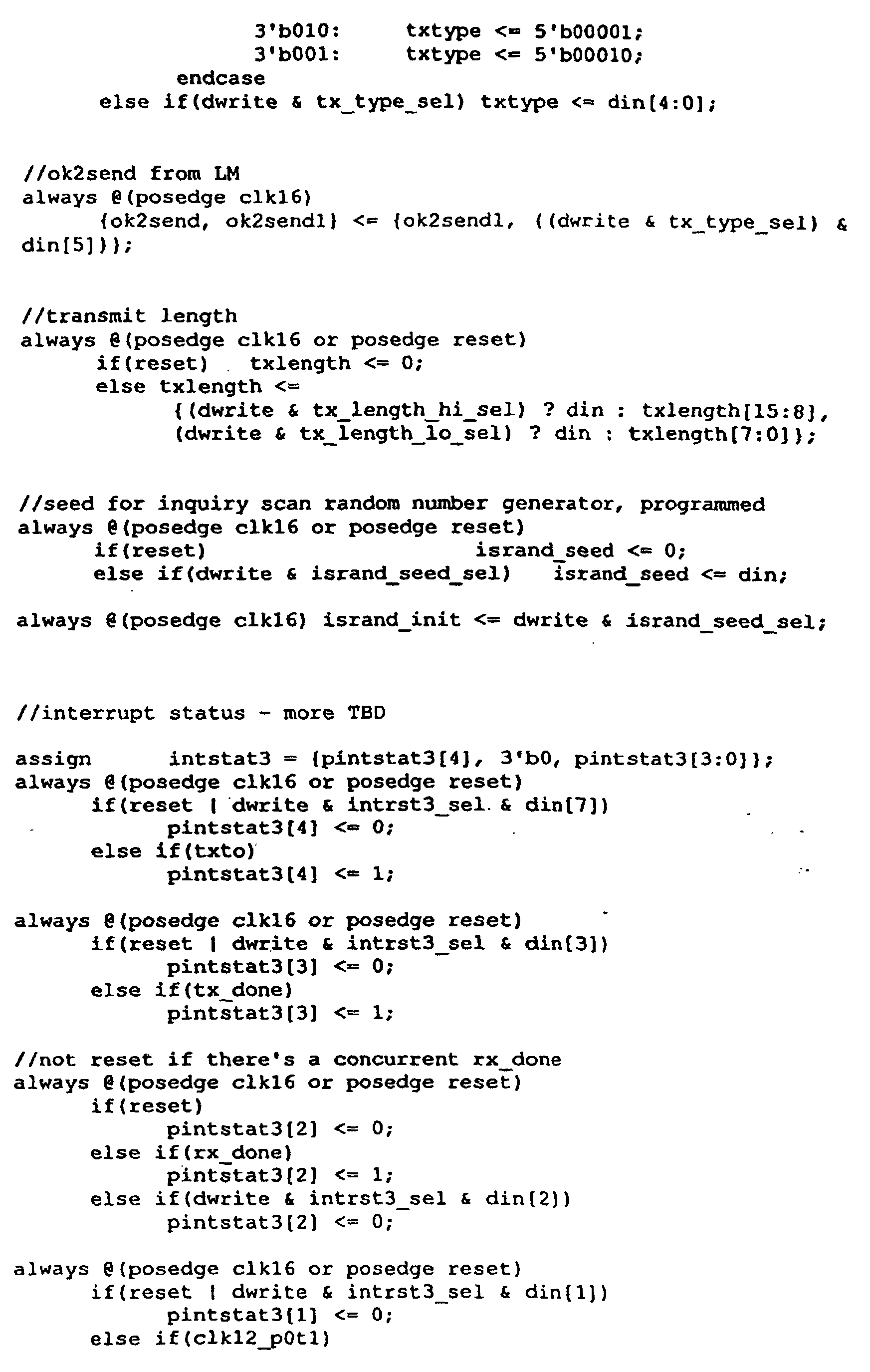
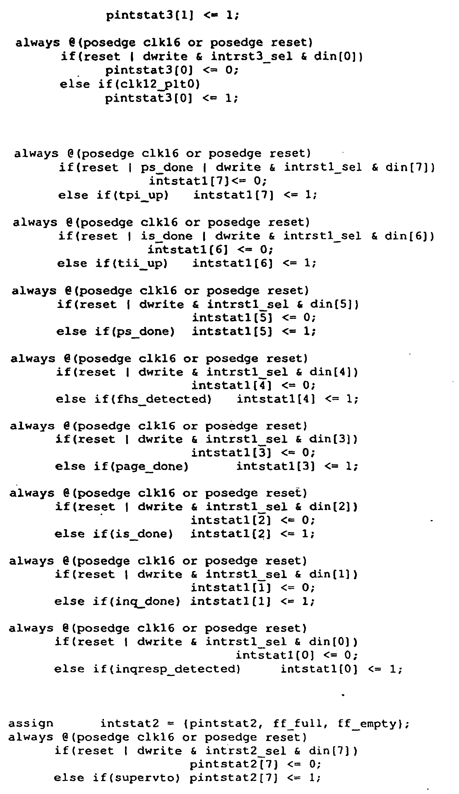


Claims (10)
- A method of performing a context switch operation, characterized by:accessing context data in a first register of a peripheral system, the first register being associated with a first index value;receiving a second index value from a host computer associated with the peripheral system;accessing context data in a second register of the peripheral system, the second register being associated with the second index value.
- The method recited in claim 1 wherein context data further is characterized by:a device address for one of a plurality of network devices;a class value;a clock offset value; andan active member address.
- The method recited in claim 1 wherein the accessing context data in a second register further is characterized by:receiving an address value that identifies an address within the second register;receiving a control input that identifies at least one of a plurality of functions, the plurality of functions including a read function and a write function;receiving, if the control input identifies the write function, a data value; andif the control input identifies the write function, writing the data value to the second register at the address identified by the address value.
- The method recited in claim 1 wherein the accessing context data in a second register further is characterized by:receiving an address value that identifies an address within the second register;receiving a read control input; andproviding the contents of the second register at the address identified by the address value to the host computer.
- The method recited in claim 1 wherein the accessing context data in a second register further is characterized by:receiving an address value that identifies an address within the second register;receiving a data value;receiving a write control input; andwriting the data value to the second register at the address identified by the address value.
- The method recited in claim 1 wherein the accessing context data further is characterized by:receiving an address value that identifies an address within the second register;receiving a control input that identifies one of a plurality of functions, the plurality of functions including a read function and a write function; andif the control input identifies the read function, providing the contents of the second register at the address identified by the address value to the host computer.
- A system, characterized by:a host computer, the host computer including a microprocessor;at least one peripheral system coupled to the host processor, the peripheral system including a first register, the first register being associated with a first index value, the peripheral system further including a second register, the second register being associated with a second index value;an interface coupled to the host computer and to the peripheral system, the interface being configured to provide the first and second index values from the host computer to the peripheral system; anda register access circuit coupled to the host computer, the register access circuit being configured to access the first register if the first index value is provided by the host computer, the register access circuit being further configured to access the second register if the second index value is provided by the host computer.
- The system recited in claim 7 wherein the peripheral system includes a state machine module, the state machine module being characterized by:an address portion;a control portion; anda data portion, the first register and the second register being included in the data portion.
- The system recited in claim 8 wherein the address portion is characterized by a register access circuit.
- The system recited in claim 7 wherein the peripheral system is characterized by a plurality of context registers, wherein each of the plurality of context registers is associated with one of a plurality of index values.
Applications Claiming Priority (2)
| Application Number | Priority Date | Filing Date | Title |
|---|---|---|---|
| US59200900A | 2000-06-12 | 2000-06-12 | |
| US592009 | 2000-06-12 |
Publications (3)
| Publication Number | Publication Date |
|---|---|
| EP1168158A2 true EP1168158A2 (en) | 2002-01-02 |
| EP1168158A3 EP1168158A3 (en) | 2006-02-01 |
| EP1168158B1 EP1168158B1 (en) | 2007-10-10 |
Family
ID=24368893
Family Applications (1)
| Application Number | Title | Priority Date | Filing Date |
|---|---|---|---|
| EP01250212A Expired - Lifetime EP1168158B1 (en) | 2000-06-12 | 2001-06-12 | Context switch architecture and system |
Country Status (3)
| Country | Link |
|---|---|
| US (1) | US20060101164A1 (en) |
| EP (1) | EP1168158B1 (en) |
| DE (1) | DE60130836T2 (en) |
Cited By (7)
| Publication number | Priority date | Publication date | Assignee | Title |
|---|---|---|---|---|
| EP1309134A1 (en) * | 2001-10-31 | 2003-05-07 | Samsung Electronics Co., Ltd. | Master for bluetooth communication and method for establishing beacon channel thereof |
| US7031270B2 (en) | 2000-10-30 | 2006-04-18 | Samsung Electronics Co., Ltd. | Master for bluetooth communication and method for establishing beacon channel thereof |
| CN108601006A (en) * | 2018-04-28 | 2018-09-28 | 上海与德通讯技术有限公司 | Instruction transmission method based on blueteeth network and system |
| US10891238B1 (en) | 2019-06-28 | 2021-01-12 | International Business Machines Corporation | Dynamically joining and splitting dynamic address translation (DAT) tables based on operational context |
| US10970224B2 (en) | 2019-06-28 | 2021-04-06 | International Business Machines Corporation | Operational context subspaces |
| US11074195B2 (en) | 2019-06-28 | 2021-07-27 | International Business Machines Corporation | Access to dynamic address translation across multiple spaces for operational context subspaces |
| US11176056B2 (en) | 2019-06-28 | 2021-11-16 | International Business Machines Corporation | Private space control within a common address space |
Families Citing this family (30)
| Publication number | Priority date | Publication date | Assignee | Title |
|---|---|---|---|---|
| FR2841669B1 (en) * | 2002-06-27 | 2006-01-06 | St Microelectronics Sa | METHOD FOR TRANSMITTING DATA PACKETS BETWEEN TWO SLAVE UNITS AND A MASTER UNIT COMPRISING TWO PROCESSORS |
| TWI328198B (en) * | 2006-12-11 | 2010-08-01 | Via Tech Inc | Gpu context switching system |
| US9486703B2 (en) * | 2007-01-31 | 2016-11-08 | Broadcom Corporation | Mobile communication device with game application for use in conjunction with a remote mobile communication device and methods for use therewith |
| US20090197641A1 (en) * | 2008-02-06 | 2009-08-06 | Broadcom Corporation | Computing device with handheld and extended computing units |
| US8121541B2 (en) * | 2007-01-31 | 2012-02-21 | Broadcom Corporation | Integrated circuit with intra-chip and extra-chip RF communication |
| US8200156B2 (en) * | 2007-01-31 | 2012-06-12 | Broadcom Corporation | Apparatus for allocation of wireless resources |
| US8254319B2 (en) * | 2007-01-31 | 2012-08-28 | Broadcom Corporation | Wireless programmable logic device |
| US8239650B2 (en) * | 2007-01-31 | 2012-08-07 | Broadcom Corporation | Wirelessly configurable memory device addressing |
| US8010735B2 (en) * | 2007-07-31 | 2011-08-30 | Broadcom Corporation | Flash memory with millimeter wave host interface and method for use therewith |
| US8204075B2 (en) * | 2007-01-31 | 2012-06-19 | Broadcom Corporation | Inter-device wireless communication for intra-device communications |
| US8280303B2 (en) * | 2007-01-31 | 2012-10-02 | Broadcom Corporation | Distributed digital signal processor |
| US20080320293A1 (en) * | 2007-01-31 | 2008-12-25 | Broadcom Corporation | Configurable processing core |
| US8223736B2 (en) * | 2007-01-31 | 2012-07-17 | Broadcom Corporation | Apparatus for managing frequency use |
| US20090011832A1 (en) * | 2007-01-31 | 2009-01-08 | Broadcom Corporation | Mobile communication device with game application for display on a remote monitor and methods for use therewith |
| US8289944B2 (en) * | 2007-01-31 | 2012-10-16 | Broadcom Corporation | Apparatus for configuration of wireless operation |
| US8116294B2 (en) * | 2007-01-31 | 2012-02-14 | Broadcom Corporation | RF bus controller |
| US8238275B2 (en) * | 2007-01-31 | 2012-08-07 | Broadcom Corporation | IC with MMW transceiver communications |
| US8125950B2 (en) * | 2007-01-31 | 2012-02-28 | Broadcom Corporation | Apparatus for wirelessly managing resources |
| US20090017910A1 (en) * | 2007-06-22 | 2009-01-15 | Broadcom Corporation | Position and motion tracking of an object |
| US8438322B2 (en) * | 2007-01-31 | 2013-05-07 | Broadcom Corporation | Processing module with millimeter wave transceiver interconnection |
| US20090037670A1 (en) * | 2007-07-30 | 2009-02-05 | Broadcom Corporation | Disk controller with millimeter wave host interface and method for use therewith |
| CN101227684B (en) * | 2008-01-28 | 2012-12-26 | 宇龙计算机通信科技(深圳)有限公司 | System and method for editing information |
| US8117370B2 (en) * | 2008-02-06 | 2012-02-14 | Broadcom Corporation | IC for handheld computing unit of a computing device |
| US20090198798A1 (en) * | 2008-02-06 | 2009-08-06 | Broadcom Corporation | Handheld computing unit back-up system |
| US8195928B2 (en) * | 2008-02-06 | 2012-06-05 | Broadcom Corporation | Handheld computing unit with merged mode |
| US8175646B2 (en) * | 2008-02-06 | 2012-05-08 | Broadcom Corporation | Networking of multiple mode handheld computing unit |
| US8717974B2 (en) * | 2008-02-06 | 2014-05-06 | Broadcom Corporation | Handheld computing unit coordination of femtocell AP functions |
| US8064952B2 (en) * | 2008-02-06 | 2011-11-22 | Broadcom Corporation | A/V control for a computing device with handheld and extended computing units |
| US8430750B2 (en) * | 2008-05-22 | 2013-04-30 | Broadcom Corporation | Video gaming device with image identification |
| KR20220070973A (en) * | 2020-11-23 | 2022-05-31 | 삼성전자주식회사 | Method for setting communication scheme and electronic device using the same |
Family Cites Families (34)
| Publication number | Priority date | Publication date | Assignee | Title |
|---|---|---|---|---|
| GB2168868A (en) * | 1984-12-19 | 1986-06-25 | Philips Electronic Associated | Polyphase filters |
| US5163016A (en) * | 1990-03-06 | 1992-11-10 | At&T Bell Laboratories | Analytical development and verification of control-intensive systems |
| US5327540A (en) * | 1991-09-18 | 1994-07-05 | Ncr Corporation | Method and apparatus for decoding bus master arbitration levels to optimize memory transfers |
| KR930013999A (en) * | 1991-12-31 | 1993-07-22 | 정몽헌 | Block control circuit of graphic controller |
| TW228043B (en) * | 1992-06-26 | 1994-08-11 | Philips Electronics Nv | |
| GB2281830B (en) * | 1993-09-11 | 1998-08-12 | Nokia Mobile Phones Ltd | I/q-modulator and i/q-demodulator |
| US5613114A (en) * | 1994-04-15 | 1997-03-18 | Apple Computer, Inc | System and method for custom context switching |
| US5655132A (en) * | 1994-08-08 | 1997-08-05 | Rockwell International Corporation | Register file with multi-tasking support |
| US5974306A (en) * | 1994-10-12 | 1999-10-26 | Hewlett-Packard Company | Time-share I-Q Mixer system with distribution switch feeding in-phase and quadrature polarity inverters |
| US5659749A (en) * | 1995-05-08 | 1997-08-19 | National Instruments Corporation | System and method for performing efficient hardware context switching in an instrumentation system |
| US5812823A (en) * | 1996-01-02 | 1998-09-22 | International Business Machines Corporation | Method and system for performing an emulation context save and restore that is transparent to the operating system |
| GB9605719D0 (en) * | 1996-03-19 | 1996-05-22 | Philips Electronics Nv | Integrated receiver |
| US6061711A (en) * | 1996-08-19 | 2000-05-09 | Samsung Electronics, Inc. | Efficient context saving and restoring in a multi-tasking computing system environment |
| US6247040B1 (en) * | 1996-09-30 | 2001-06-12 | Lsi Logic Corporation | Method and structure for automated switching between multiple contexts in a storage subsystem target device |
| US5926646A (en) * | 1997-09-11 | 1999-07-20 | Advanced Micro Devices, Inc. | Context-dependent memory-mapped registers for transparent expansion of a register file |
| US6026297A (en) * | 1997-09-17 | 2000-02-15 | Telefonaktiebolaget Lm Ericsson | Contemporaneous connectivity to multiple piconets |
| US5903919A (en) * | 1997-10-07 | 1999-05-11 | Motorola, Inc. | Method and apparatus for selecting a register bank |
| JPH11163970A (en) * | 1997-11-28 | 1999-06-18 | Oki Electric Ind Co Ltd | Equipment base control system |
| US6041176A (en) * | 1998-02-27 | 2000-03-21 | Texas Instruments Incorporated | Emulation devices utilizing state machines |
| US6128672A (en) * | 1998-03-10 | 2000-10-03 | Motorola, Inc. | Data transfer using software interrupt service routine between host processor and external device with queue of host processor and hardware queue pointers on external device |
| US6188411B1 (en) * | 1998-07-02 | 2001-02-13 | Neomagic Corp. | Closed-loop reading of index registers using wide read and narrow write for multi-threaded system |
| SE9803632D0 (en) * | 1998-10-22 | 1998-10-22 | Ericsson Telefon Ab L M | A processor |
| US6154832A (en) * | 1998-12-04 | 2000-11-28 | Advanced Micro Devices, Inc. | Processor employing multiple register sets to eliminate interrupts |
| US6883171B1 (en) * | 1999-06-02 | 2005-04-19 | Microsoft Corporation | Dynamic address windowing on a PCI bus |
| US6169745B1 (en) * | 1999-06-18 | 2001-01-02 | Sony Corporation | System and method for multi-level context switching in an electronic network |
| US6393500B1 (en) * | 1999-08-12 | 2002-05-21 | Mips Technologies, Inc. | Burst-configurable data bus |
| US6751737B1 (en) * | 1999-10-07 | 2004-06-15 | Advanced Micro Devices | Multiple protected mode execution environments using multiple register sets and meta-protected instructions |
| US6314486B1 (en) * | 1999-10-15 | 2001-11-06 | Sun Microsystems, Inc. | Data transfer with JTAG controller using index register to specipy one of several control/status registers for access in read and write operations with data register |
| US6683886B1 (en) * | 1999-10-19 | 2004-01-27 | Koninklijke Philips Electronics N.V. | Bluetooth communication units, wireless communication systems, wireless communication devices, bluetooth communications methods, and wireless communication methods |
| US6975613B1 (en) * | 1999-12-06 | 2005-12-13 | Telefonaktiebolaget L M Ericsson (Publ) | System and method for scheduling communication sessions in an ad-hoc network |
| US6405027B1 (en) * | 1999-12-08 | 2002-06-11 | Philips Electronics N.A. Corporation | Group call for a wireless mobile communication device using bluetooth |
| US6560449B1 (en) * | 2000-06-12 | 2003-05-06 | Broadcom Corporation | Image-rejection I/Q demodulators |
| US6650880B1 (en) * | 2000-06-12 | 2003-11-18 | Broadcom Corporation | Wireless data communications using FIFO for synchronization memory |
| US6778594B1 (en) * | 2000-06-12 | 2004-08-17 | Broadcom Corporation | Receiver architecture employing low intermediate frequency and complex filtering |
-
2001
- 2001-06-12 EP EP01250212A patent/EP1168158B1/en not_active Expired - Lifetime
- 2001-06-12 DE DE60130836T patent/DE60130836T2/en not_active Expired - Fee Related
-
2005
- 2005-12-20 US US11/314,036 patent/US20060101164A1/en not_active Abandoned
Cited By (8)
| Publication number | Priority date | Publication date | Assignee | Title |
|---|---|---|---|---|
| US7031270B2 (en) | 2000-10-30 | 2006-04-18 | Samsung Electronics Co., Ltd. | Master for bluetooth communication and method for establishing beacon channel thereof |
| EP1309134A1 (en) * | 2001-10-31 | 2003-05-07 | Samsung Electronics Co., Ltd. | Master for bluetooth communication and method for establishing beacon channel thereof |
| CN108601006A (en) * | 2018-04-28 | 2018-09-28 | 上海与德通讯技术有限公司 | Instruction transmission method based on blueteeth network and system |
| US10891238B1 (en) | 2019-06-28 | 2021-01-12 | International Business Machines Corporation | Dynamically joining and splitting dynamic address translation (DAT) tables based on operational context |
| US10970224B2 (en) | 2019-06-28 | 2021-04-06 | International Business Machines Corporation | Operational context subspaces |
| US11074195B2 (en) | 2019-06-28 | 2021-07-27 | International Business Machines Corporation | Access to dynamic address translation across multiple spaces for operational context subspaces |
| US11176056B2 (en) | 2019-06-28 | 2021-11-16 | International Business Machines Corporation | Private space control within a common address space |
| US11321239B2 (en) | 2019-06-28 | 2022-05-03 | International Business Machines Corporation | Dynamically joining and splitting dynamic address translation (DAT) tables based on operational context |
Also Published As
| Publication number | Publication date |
|---|---|
| EP1168158A3 (en) | 2006-02-01 |
| DE60130836T2 (en) | 2008-07-17 |
| DE60130836D1 (en) | 2007-11-22 |
| US20060101164A1 (en) | 2006-05-11 |
| EP1168158B1 (en) | 2007-10-10 |
Similar Documents
| Publication | Publication Date | Title |
|---|---|---|
| US20060101164A1 (en) | Context switch architecture and system | |
| FI111309B (en) | A terminal connected to a telecommunications network by radio | |
| CN100412848C (en) | Computer Networks and Computer Systems | |
| EP1640862B1 (en) | Concurrence management program, storage medium containing the concurrence management program, concurrence management method, and electronic device | |
| CN1496516B (en) | Resource dedication system and method for computer architecture for broadband networks | |
| US20040054997A1 (en) | Task definition for specifying resource requirements | |
| US8387056B2 (en) | Method for dynamically enabling the expansion of a computer operating system | |
| CN101141742B (en) | Application communication method of terminal | |
| WO2002077826A1 (en) | Memory protection system and method for computer architecture for broadband networks | |
| EP1370969A1 (en) | System and method for data synchronization for a computer architecture for broadband networks | |
| US20050068913A1 (en) | Metaspace: communication middleware for partially connected mobile ad hoc networks | |
| JP2012513162A (en) | Wireless access point that supports control by multiple applications | |
| JPH10340128A (en) | Data processing device and mobile communication terminal device | |
| CN116954952B (en) | An adaptive hybrid communication method, device, medium and equipment for robots | |
| JP2008538043A (en) | Technology for setting events in a multithreaded system | |
| CN103324529B (en) | Across task sharing operating system subprocess | |
| CN101005673A (en) | Method for realizing simultaneously stand-by in double mode mobile phone | |
| CN121326789A (en) | Memory management method, device and medium based on dynamic mapping | |
| CN112654079A (en) | Symbol turn-off method and device | |
| CN113867681B (en) | Data processing methods and devices, data processing equipment and storage media | |
| WO2023207947A1 (en) | Cell reconfiguration method, apparatus, terminal, and network side device | |
| CN119166381B (en) | Method and terminal device for application connection | |
| JP2012088906A (en) | Electronic device and control method for the same | |
| GB2402842A (en) | Mobile radio communications device. | |
| CN113260029A (en) | Terminal device, network side device and communication method |
Legal Events
| Date | Code | Title | Description |
|---|---|---|---|
| PUAI | Public reference made under article 153(3) epc to a published international application that has entered the european phase |
Free format text: ORIGINAL CODE: 0009012 |
|
| AK | Designated contracting states |
Kind code of ref document: A2 Designated state(s): AT BE CH CY DE DK ES FI FR GB GR IE IT LI LU MC NL PT SE TR |
|
| AX | Request for extension of the european patent |
Free format text: AL;LT;LV;MK;RO;SI |
|
| 17P | Request for examination filed |
Effective date: 20020802 |
|
| PUAL | Search report despatched |
Free format text: ORIGINAL CODE: 0009013 |
|
| AK | Designated contracting states |
Kind code of ref document: A3 Designated state(s): AT BE CH CY DE DK ES FI FR GB GR IE IT LI LU MC NL PT SE TR |
|
| AX | Request for extension of the european patent |
Extension state: AL LT LV MK RO SI |
|
| RIC1 | Information provided on ipc code assigned before grant |
Ipc: G06F 9/48 20060101AFI20051215BHEP |
|
| AKX | Designation fees paid |
Designated state(s): DE FR GB |
|
| 17Q | First examination report despatched |
Effective date: 20060307 |
|
| GRAP | Despatch of communication of intention to grant a patent |
Free format text: ORIGINAL CODE: EPIDOSNIGR1 |
|
| RAP1 | Party data changed (applicant data changed or rights of an application transferred) |
Owner name: BROADCOM CORPORATION |
|
| GRAS | Grant fee paid |
Free format text: ORIGINAL CODE: EPIDOSNIGR3 |
|
| GRAA | (expected) grant |
Free format text: ORIGINAL CODE: 0009210 |
|
| AK | Designated contracting states |
Kind code of ref document: B1 Designated state(s): DE FR GB |
|
| REG | Reference to a national code |
Ref country code: GB Ref legal event code: FG4D |
|
| REF | Corresponds to: |
Ref document number: 60130836 Country of ref document: DE Date of ref document: 20071122 Kind code of ref document: P |
|
| EN | Fr: translation not filed | ||
| PLBE | No opposition filed within time limit |
Free format text: ORIGINAL CODE: 0009261 |
|
| STAA | Information on the status of an ep patent application or granted ep patent |
Free format text: STATUS: NO OPPOSITION FILED WITHIN TIME LIMIT |
|
| 26N | No opposition filed |
Effective date: 20080711 |
|
| PG25 | Lapsed in a contracting state [announced via postgrant information from national office to epo] |
Ref country code: FR Free format text: LAPSE BECAUSE OF FAILURE TO SUBMIT A TRANSLATION OF THE DESCRIPTION OR TO PAY THE FEE WITHIN THE PRESCRIBED TIME-LIMIT Effective date: 20080725 |
|
| PGFP | Annual fee paid to national office [announced via postgrant information from national office to epo] |
Ref country code: DE Payment date: 20090630 Year of fee payment: 9 Ref country code: GB Payment date: 20090623 Year of fee payment: 9 |
|
| GBPC | Gb: european patent ceased through non-payment of renewal fee |
Effective date: 20100612 |
|
| PG25 | Lapsed in a contracting state [announced via postgrant information from national office to epo] |
Ref country code: DE Free format text: LAPSE BECAUSE OF NON-PAYMENT OF DUE FEES Effective date: 20110101 |
|
| PG25 | Lapsed in a contracting state [announced via postgrant information from national office to epo] |
Ref country code: GB Free format text: LAPSE BECAUSE OF NON-PAYMENT OF DUE FEES Effective date: 20100612 |