EP1164495A2 - Integrated circuit for modem - Google Patents
Integrated circuit for modem Download PDFInfo
- Publication number
- EP1164495A2 EP1164495A2 EP01113923A EP01113923A EP1164495A2 EP 1164495 A2 EP1164495 A2 EP 1164495A2 EP 01113923 A EP01113923 A EP 01113923A EP 01113923 A EP01113923 A EP 01113923A EP 1164495 A2 EP1164495 A2 EP 1164495A2
- Authority
- EP
- European Patent Office
- Prior art keywords
- ram
- instruction
- hardware unit
- interleave
- banks
- Prior art date
- Legal status (The legal status is an assumption and is not a legal conclusion. Google has not performed a legal analysis and makes no representation as to the accuracy of the status listed.)
- Withdrawn
Links
Images



Classifications
-
- G—PHYSICS
- G06—COMPUTING OR CALCULATING; COUNTING
- G06F—ELECTRIC DIGITAL DATA PROCESSING
- G06F9/00—Arrangements for program control, e.g. control units
- G06F9/06—Arrangements for program control, e.g. control units using stored programs, i.e. using an internal store of processing equipment to receive or retain programs
- G06F9/30—Arrangements for executing machine instructions, e.g. instruction decode
- G06F9/38—Concurrent instruction execution, e.g. pipeline or look ahead
- G06F9/3802—Instruction prefetching
- G06F9/3814—Implementation provisions of instruction buffers, e.g. prefetch buffer; banks
-
- G—PHYSICS
- G06—COMPUTING OR CALCULATING; COUNTING
- G06F—ELECTRIC DIGITAL DATA PROCESSING
- G06F12/00—Accessing, addressing or allocating within memory systems or architectures
- G06F12/02—Addressing or allocation; Relocation
- G06F12/08—Addressing or allocation; Relocation in hierarchically structured memory systems, e.g. virtual memory systems
- G06F12/0802—Addressing of a memory level in which the access to the desired data or data block requires associative addressing means, e.g. caches
- G06F12/0844—Multiple simultaneous or quasi-simultaneous cache accessing
- G06F12/0846—Cache with multiple tag or data arrays being simultaneously accessible
- G06F12/0851—Cache with interleaved addressing
-
- G—PHYSICS
- G06—COMPUTING OR CALCULATING; COUNTING
- G06F—ELECTRIC DIGITAL DATA PROCESSING
- G06F12/00—Accessing, addressing or allocating within memory systems or architectures
- G06F12/02—Addressing or allocation; Relocation
- G06F12/08—Addressing or allocation; Relocation in hierarchically structured memory systems, e.g. virtual memory systems
- G06F12/10—Address translation
- G06F12/1027—Address translation using associative or pseudo-associative address translation means, e.g. translation look-aside buffer [TLB]
- G06F12/1045—Address translation using associative or pseudo-associative address translation means, e.g. translation look-aside buffer [TLB] associated with a data cache
-
- G—PHYSICS
- G06—COMPUTING OR CALCULATING; COUNTING
- G06F—ELECTRIC DIGITAL DATA PROCESSING
- G06F15/00—Digital computers in general; Data processing equipment in general
- G06F15/76—Architectures of general purpose stored program computers
- G06F15/78—Architectures of general purpose stored program computers comprising a single central processing unit
- G06F15/7839—Architectures of general purpose stored program computers comprising a single central processing unit with memory
- G06F15/7842—Architectures of general purpose stored program computers comprising a single central processing unit with memory on one IC chip (single chip microcontrollers)
- G06F15/7846—On-chip cache and off-chip main memory
-
- G—PHYSICS
- G06—COMPUTING OR CALCULATING; COUNTING
- G06F—ELECTRIC DIGITAL DATA PROCESSING
- G06F15/00—Digital computers in general; Data processing equipment in general
- G06F15/76—Architectures of general purpose stored program computers
- G06F15/78—Architectures of general purpose stored program computers comprising a single central processing unit
- G06F15/7839—Architectures of general purpose stored program computers comprising a single central processing unit with memory
- G06F15/7842—Architectures of general purpose stored program computers comprising a single central processing unit with memory on one IC chip (single chip microcontrollers)
- G06F15/7857—Architectures of general purpose stored program computers comprising a single central processing unit with memory on one IC chip (single chip microcontrollers) using interleaved memory
-
- G—PHYSICS
- G06—COMPUTING OR CALCULATING; COUNTING
- G06F—ELECTRIC DIGITAL DATA PROCESSING
- G06F9/00—Arrangements for program control, e.g. control units
- G06F9/06—Arrangements for program control, e.g. control units using stored programs, i.e. using an internal store of processing equipment to receive or retain programs
- G06F9/30—Arrangements for executing machine instructions, e.g. instruction decode
- G06F9/38—Concurrent instruction execution, e.g. pipeline or look ahead
- G06F9/3802—Instruction prefetching
Definitions
- the present invention relates to an integrated circuit for modem and in particular to an integrated circuit for modem including an instruction RAM which is in plural bank configuration and functions as a cache memory for an external instruction ROM.
- FIG. 4 shows a block diagram of an exemplary configuration of such prior art integrated circuit for modem.
- such type of integrated circuit for modem comprises a hardware unit 1, instruction RAM 2, CPU 3, work RAM 4, and RAM controller 5.
- the hardware unit 1 comprises a framing circuit 11, error correction circuit 12, interleave circuit 13, interleave RAM 14 and digital signal processing circuit 15 and conducts baseband processing and digital modulation and demodulation for transmission and reception data between externally connected D/A or A/D convertor and device.
- the framing circuit 11 conducts framing and deframing for transmission and reception data in a form of ADSL standard.
- the error correction circuit 12 conducts addition of an error correcting code to the transmission and reception data or the error correction therefor.
- the interleave circuit conducts interleaving and deinterleaving for transmission and reception data.
- the interleave RAM 14 is an interleave processing memory which is accessed by the interleave circuit 13.
- the digital signal processing circuit 15 conducts digital modulation and demodulation for transmission and reception data.
- the instruction RAM 2 is a memory having a configuration of 1K word by 8 banks and functions as a cache memory for the external instruction RAM which prefetches on a bank basis instructions from externally connected instruction ROM.
- the CPU 3 executes instructions, which are prefetched from the external instruction ROM to the instruction RAM 2 for controlling the hardware unit 1.
- the work RAM 4 is a memory, which is accessed for working.
- the RAM controller 5 comprises a prefetch control circuit and control register.
- the prefetch control circuit causes the instructions to be prefetched from the external instruction ROM to the instruction RAM 2 on a bank basis for controlling the instruction RAM 2 so that they function as a cache memory for the external instruction ROM.
- the CPU 3 presets commands in the control register. Control in the RAM controller 5 is conducted in response to the preset content.
- the instructions which are stored in the external instruction ROM are prefetched to the instruction RAM 2 on a bank basis by the RAM controller 5.
- the CPU 3 executes the instruction, which has been prefetched, to the instruction RAM 2 so that the hardware unit 1 is controlled.
- the instruction RAM 2 functions as the cache memory for the external instruction ROM.
- the CPU is capable of executing instructions at a high rate at the access time to the instruction RAM 2 rather than the access time to the external instruction ROM so that it is capable of processing the control of the hardware unit 1.
- the base band processing such as framing, error correction, interleaving, and digital modulation and demodulation is also conducted for the transmission and reception data in a parallel manner by each of the circuits 11 to 15 in the hardware unit 1.
- the cache operation of the instruction RAM and the parallel operation in the hardware unit implement a high rate communications modem such as ADSL modem.
- an object of the present invention is to reduce the circuit area of the integrated circuit for modem to achieve the reduction in the manufacturing cost.
- an integrated circuit for modem including a hardware unit for conducting an error correction processing, interleave processing and digital signal processing for transmission and reception data; an instruction RAM comprising a plurality of banks, which functions as a cache memory of an external instruction RAM; and a CPU which executes an instruction which is prefetched to the instruction RAM for controlling the hardware unit, characterized in that the CPU and the hardware time-divisionally share part of the banks of the instruction RAM.
- the hardware unit divides the banks of the instruction RAM and uses part of the banks of the instruction RAM as a memory for interleave processing.
- the circuit comprises an RAM controller which conducts controlling so that instructions are prefetched from the external instruction ROM to the instruction RAM on a bank basis to cause the instruction RAM to function as a cache memory of the external instruction ROM and conducts controlling to cause the CPU and the hardware unit to time-divisionally share part of the banks of the instruction RAM.
- the RAM controller receives data, address and write control signal from an interleave RAM interface of the hardware unit and outputs them to part of the banks of the instruction RAM and outputs them to an interleave RAM interface of the hardware unit by selecting the data output of part of the banks of the hardware unit during the transmission and reception of the data.
- the RAM controller comprises
- the RAM controller comprises a control register in which commands which are preset by the CPU are stored and in which the connection switching signal is generated corresponding to the content of control register.
- Fig. 1 is a block diagram showing an embodiment of the integrated circuit for modem of the present invention.
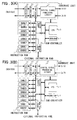
- Fig. 2 is a circuit diagram showing the configuration of the RAM controller 5 and the instruction RAM 2 in the integrated circuit for modem, which is shown in Fig. 1.
- Fig. 3 is an explanatory view explaining the operation of the RAM controller 5 in the integrated circuit for modem in Fig. 1.
- Fig. 4 is a block diagram showing the exemplary configuration.
- Fig. 1 is a block diagram showing a mode of embodying the integrated circuit for modem of the present invention.
- the integrated circuit for modem of the present embodiment comprises a hardware unit 1, instruction RAM 2, CPU 3, work RAM 4 and RAM controller 5 as is similar to the prior art integrated circuit for modem.
- the integrated circuit for modem of the present invention is different from the prior art integrated circuit for modem in that the hardware unit 1 does not include any interleave RAM and in that the RAM controller 5 is connected to the interleave RAM interface of the interleave circuit 13 of the hardware unit 1. Since the blocks 2 to 4, 11, to 13, 14 are identical to those in the prior art integrated circuit for modem excepting the RAM controller, description of them will be omitted herein for simplicity of description.
- the RAM controller 5 performs such a control that the instructions are prefetched from the external instruction ROM to the instruction RAM 2 on a bank basis and the instruction RAM 2 is caused to operate as a cache memory for the external instruction ROM and the CPU and the hardware unit 1 are caused to the time-divisionally share part of banks of the instruction RAM 2.
- Fig. 2 is a circuit diagram showing the configuration of the RAM controller 5 and the instruction RAM 2 in detail.
- the RAM controller 5 performs such a control that instructions are prefetched from the external instruction ROM to the instruction RAM 2 on a bank basis by means of a prefetch control circuit as is similar to the prior art to cause the instruction RAM 2 to operate as a cache memory of the external instruction ROM and performs connection control to switch the banks 4 to 7 of the instruction RAM 2 to connect the interleave RAM interface of the hardware unit 1 in response to a connection switching signal which is activated under control of CPU 3.
- Main block for the switching connection control comprises a higher order address to which high order addresses are input from an interleave RAM interface of the hardware unit and decoded are from which a bank selection signal for the interleave RAM is output; a gate circuit to which a write control signal is input from an interleave RAM interface of the hardware unit and which is controlled by the bank selection signal for outputting a bank write control signal for the interleave RAM therefrom; a (first) multiplexer to which data is input from the interleave RAM interface of the hardware unit and which switches to part of the banks of the instruction RAM in response to a connection switching signal for outputting data thereto; a (second) multiplexer to which an address and the bank write control signal are input from the interleave RAM interface of the hardware unit and the gate circuit and switches to part of the banks of the instruction RAM in response to the connection switching signal for outputting them thereto; and a selector which selects an data output from the part of the banks of the instruction RAM in response to the bank selection signal and to output the data to
- Fig. 3 is an explanatory view explaining the operation of the RAM controller 5 in the integrated circuit for modem in the present embodiment, schematically showing the connection condition of the banks of the instruction RAM 2 in the RAM controller 5. The operation of the integrated circuit for modem of the present embodiment will be described with reference to Fig. 3.
- ADSL modems and the like following initialization sequence processing is conducted between modems which will communicate to each other prior to starting the data transmission and reception.
- the CPU 2 in the integrated circuit for modem controls the digital signal processing circuit 15 of the hardware unit 1 within a predetermined period of time and reads out received signals from the digital signal processing circuit 15 of the hardware unit 1 for conducting various calculations.
- the interleave circuit 13 of the hardware unit 1 does not operate so that the interleave RAM is not necessary while the amount of the data which is processed by the CPU 3 is large. Accordingly, as shown in Fig. 3(A), in the RAM controller 5, all of the banks of the instruction RAM 2 interfaces with the CPU bus or the prefetch control circuit and all of the banks of the instruction RAM 2 operate as a cache memory as is similar to the case with prior art.
- the CPU 2 in the integrated circuit for modem mainly conducts monitor processing for detecting the abnormal conditions of the transmission and reception in the hardware unit 2.
- the interleave circuit 13 of the hardware unit 1 Since the data is being transmitted or received during this monitor processing, the interleave circuit 13 of the hardware unit 1 operates so that the interleave RAM is necessary. On the other hand, the rate of the data, which is processed by the CPU 3, is less than that in the above-mentioned initialization sequence processing. Accordingly, the connection switching signal is activated under control of the CPU 3 in the RAM controller 5 as shown in Fig. 3(B) so that the banks 4 to 7 of the instruction RAM 2 is switched so that it is connected to the interleave RAM interface of the hardware unit 1.
- the banks 0 to 3 of the instruction RAM 2 are interfaced with the CPU bus or the prefetch control circuit so that it functions as a cache memory.
- the integrated circuit for modem of this embodiment performs cache operation of the instruction RAM and parallel processing in the hardware unit similarly to the case with prior art and has the same functions and performances as those of the prior art and is capable of reducing the capacity of the RAM to be used and of implementing high rate communications modem such as ADSL modems and the like.
- the integrated circuit for modem of the present invention have advantages that it can reduce the capacity of the RAM to be used and it can be manufactured at low cost.
- the reason resides in that part of the banks of the instruction RAM operating as the cache memory for the external instruction ROM is shared for use as the interleave RAM during transmission and reception of the data.
Landscapes
- Engineering & Computer Science (AREA)
- Theoretical Computer Science (AREA)
- Physics & Mathematics (AREA)
- General Engineering & Computer Science (AREA)
- General Physics & Mathematics (AREA)
- Computer Hardware Design (AREA)
- Software Systems (AREA)
- Memory System Of A Hierarchy Structure (AREA)
- Microcomputers (AREA)
- Communication Control (AREA)
Abstract
Description
As mentioned above, the integrated circuit for modem of the present invention have advantages that it can reduce the capacity of the RAM to be used and it can be manufactured at low cost.
Claims (6)
- An integrated circuit for modem including:a hardware unit for conducting an error correction processing, interleave processing and digital signal processing for transmission and reception data;an instruction RAM comprising a plurality of banks, which functions as a cache memory of an external instruction RAM; anda CPU which executes an instruction which is prefetched to the instruction RAM for controlling said hardware unit, characterized in that said CPU and said hardware time-divisionally share part of the banks of said instruction RAM.
- An integrated circuit for modem as defined in Claim 1 in which said hardware unit divides the banks of said instruction RAM and uses part of the banks of said instruction RAM as a memory for interleave processing.
- An integrated circuit as defined in Claim 1 or 2 in which said circuit comprises an RAM controller which conducts controlling so that instructions are prefetched from said external instruction ROM to said instruction RAM on a bank basis to cause said instruction RAM to function as a cache memory of said external instruction ROM and conducts controlling to cause said CPU and said hardware unit to time-divisionally share part of the banks of said instruction RAM.
- An integrated circuit for modem as defined in Claim 3 in which said RAM controller receives data, address and write control signal from an interleave RAM interface of said hardware unit and outputs them to part of the banks of said instruction RAM and outputs them to an interleave RAM interface of said hardware unit by selecting the data output of part of the banks of said hardware unit during the transmission and reception of the data.
- An integrated circuit for modem as defined in Claim 3 or 4 in which said RAM controller comprisesa higher order address to which high order addresses are input from an interleave RAM interface of said hardware unit and are decoded and from which a bank selection signal for the interleave RAM is output;a gate circuit to which a write control signal is input from the interleave RAM interface of said hardware unit and which is controlled by said bank selection signal for outputting a bank write control signal for the interleave RAM therefrom;a (first) multiplexer to which data is input from the interleave RAM interface of said hardware unit and which switches to part of the banks of said instruction RAM in response to a connection switching signal for outputting data thereto;a (second) multiplexer to which an address and said bank write control signal are input from the interleave RAM interface of said hardware unit and said gate circuit and switches to part of the banks of said instruction RAM in response to said connection switching signal for outputting them thereto; anda selector which selects a data output from the part of the banks of said instruction RAM in response to said bank selection signal and to output the data to the interleave RAM interface of said hardware unit.
- An integrated circuit for modem as defined in one of Claims 3 to 5 in which said RAM controller comprises a control register in which commands which are preset by said CPU are stored and in which said connection switching signal is generated corresponding to the content of control register.
Applications Claiming Priority (2)
| Application Number | Priority Date | Filing Date | Title |
|---|---|---|---|
| JP2000170327 | 2000-06-07 | ||
| JP2000170327A JP2001352358A (en) | 2000-06-07 | 2000-06-07 | Integrated circuit for modem |
Publications (2)
| Publication Number | Publication Date |
|---|---|
| EP1164495A2 true EP1164495A2 (en) | 2001-12-19 |
| EP1164495A3 EP1164495A3 (en) | 2004-11-10 |
Family
ID=18673062
Family Applications (1)
| Application Number | Title | Priority Date | Filing Date |
|---|---|---|---|
| EP01113923A Withdrawn EP1164495A3 (en) | 2000-06-07 | 2001-06-07 | Integrated circuit for modem |
Country Status (3)
| Country | Link |
|---|---|
| US (1) | US20010052047A1 (en) |
| EP (1) | EP1164495A3 (en) |
| JP (1) | JP2001352358A (en) |
Cited By (4)
| Publication number | Priority date | Publication date | Assignee | Title |
|---|---|---|---|---|
| WO2006004875A1 (en) * | 2004-06-30 | 2006-01-12 | Sun Microsystems, Inc. | Multiple-core processor with support for multiple virtual processors |
| WO2007052181A1 (en) * | 2005-11-02 | 2007-05-10 | Nxp B.V. | System-on-chip apparatus with time shareable memory and method for operating such an apparatus |
| US7685354B1 (en) | 2004-06-30 | 2010-03-23 | Sun Microsystems, Inc. | Multiple-core processor with flexible mapping of processor cores to cache banks |
| US11868262B2 (en) | 2018-09-11 | 2024-01-09 | Marvell Asia Pte, Ltd. | Methods and systems for distributing memory requests |
Families Citing this family (2)
| Publication number | Priority date | Publication date | Assignee | Title |
|---|---|---|---|---|
| US6728159B2 (en) * | 2001-12-21 | 2004-04-27 | International Business Machines Corporation | Flexible multibanking interface for embedded memory applications |
| FR2920584B1 (en) * | 2007-08-29 | 2009-11-13 | Commissariat Energie Atomique | SHARED MEMORY |
Family Cites Families (6)
| Publication number | Priority date | Publication date | Assignee | Title |
|---|---|---|---|---|
| US5172379A (en) * | 1989-02-24 | 1992-12-15 | Data General Corporation | High performance memory system |
| US5239654A (en) * | 1989-11-17 | 1993-08-24 | Texas Instruments Incorporated | Dual mode SIMD/MIMD processor providing reuse of MIMD instruction memories as data memories when operating in SIMD mode |
| US5335234A (en) * | 1990-06-19 | 1994-08-02 | Dell Usa, L.P. | Error correction code pipeline for interleaved memory system |
| US5761695A (en) * | 1995-09-19 | 1998-06-02 | Hitachi, Ltd. | Cache memory control method and apparatus, and method and apparatus for controlling memory capable of interleave control |
| US6044206A (en) * | 1997-10-14 | 2000-03-28 | C-Cube Microsystems | Out of order instruction processing using dual memory banks |
| US5951677A (en) * | 1998-05-29 | 1999-09-14 | Texas Instruments Incorporated | Efficient hardware implementation of euclidean array processing in reed-solomon decoding |
-
2000
- 2000-06-07 JP JP2000170327A patent/JP2001352358A/en active Pending
-
2001
- 2001-06-04 US US09/873,649 patent/US20010052047A1/en not_active Abandoned
- 2001-06-07 EP EP01113923A patent/EP1164495A3/en not_active Withdrawn
Cited By (5)
| Publication number | Priority date | Publication date | Assignee | Title |
|---|---|---|---|---|
| WO2006004875A1 (en) * | 2004-06-30 | 2006-01-12 | Sun Microsystems, Inc. | Multiple-core processor with support for multiple virtual processors |
| US7685354B1 (en) | 2004-06-30 | 2010-03-23 | Sun Microsystems, Inc. | Multiple-core processor with flexible mapping of processor cores to cache banks |
| US7873776B2 (en) | 2004-06-30 | 2011-01-18 | Oracle America, Inc. | Multiple-core processor with support for multiple virtual processors |
| WO2007052181A1 (en) * | 2005-11-02 | 2007-05-10 | Nxp B.V. | System-on-chip apparatus with time shareable memory and method for operating such an apparatus |
| US11868262B2 (en) | 2018-09-11 | 2024-01-09 | Marvell Asia Pte, Ltd. | Methods and systems for distributing memory requests |
Also Published As
| Publication number | Publication date |
|---|---|
| US20010052047A1 (en) | 2001-12-13 |
| JP2001352358A (en) | 2001-12-21 |
| EP1164495A3 (en) | 2004-11-10 |
Similar Documents
| Publication | Publication Date | Title |
|---|---|---|
| EP2212802B1 (en) | Ethernet controller | |
| EP1164495A2 (en) | Integrated circuit for modem | |
| US6578112B2 (en) | Cache memory control device for multi-processor system | |
| US20040019748A1 (en) | Memory controller which increases bus bandwidth, data transmission method using the same, and computer system having the same | |
| US20060200630A1 (en) | Embedded system with instruction prefetching device, and method for fetching instructions in embedded systems | |
| JP3778181B2 (en) | Display control device | |
| JP4005675B2 (en) | Telecommunications equipment | |
| KR20060072212A (en) | computer | |
| JP2890660B2 (en) | Bit select output port and output device | |
| KR100560566B1 (en) | Electronic exchange control board | |
| US7133979B2 (en) | Method of transferring data between a first device and a second device while manipulating at least one quantity in dependence on an address | |
| JP3748258B2 (en) | Crossbar circuit of interprocessor communication control device and computer system using the same | |
| CN116521264A (en) | Serial port configuration method, serial port configuration device, communication module and storage medium | |
| KR20050081940A (en) | Apparatus and method for controlling wire or wireless integrated lan in personal computer | |
| JP4070806B2 (en) | Television equipment | |
| EP0723683B1 (en) | Digital communication unit monitoring | |
| KR100240963B1 (en) | Plc apparatus and control method | |
| KR100597752B1 (en) | Device with bootstrap function, electronic device including same and control method | |
| KR0183831B1 (en) | Data buffering device | |
| KR100281121B1 (en) | Microprocessor | |
| JP2006172240A (en) | Data processing system and memory control method for the same | |
| JP3963039B2 (en) | Communication device | |
| JP2000010915A (en) | Communication control circuit | |
| JPH0535665A (en) | Data transfer system | |
| JPH05316168A (en) | Multi-channel multiplex communication controller |
Legal Events
| Date | Code | Title | Description |
|---|---|---|---|
| PUAI | Public reference made under article 153(3) epc to a published international application that has entered the european phase |
Free format text: ORIGINAL CODE: 0009012 |
|
| AK | Designated contracting states |
Kind code of ref document: A2 Designated state(s): AT BE CH CY DE DK ES FI FR GB GR IE IT LI LU MC NL PT SE TR |
|
| AX | Request for extension of the european patent |
Free format text: AL;LT;LV;MK;RO;SI |
|
| RAP1 | Party data changed (applicant data changed or rights of an application transferred) |
Owner name: NEC ELECTRONICS CORPORATION |
|
| PUAL | Search report despatched |
Free format text: ORIGINAL CODE: 0009013 |
|
| AK | Designated contracting states |
Kind code of ref document: A3 Designated state(s): AT BE CH CY DE DK ES FI FR GB GR IE IT LI LU MC NL PT SE TR |
|
| AX | Request for extension of the european patent |
Extension state: AL LT LV MK RO SI |
|
| RIC1 | Information provided on ipc code assigned before grant |
Ipc: 7G 06F 9/38 B Ipc: 7G 06F 12/08 B Ipc: 7G 06F 15/78 A |
|
| 17P | Request for examination filed |
Effective date: 20050304 |
|
| 17Q | First examination report despatched |
Effective date: 20050609 |
|
| AKX | Designation fees paid |
Designated state(s): DE GB |
|
| STAA | Information on the status of an ep patent application or granted ep patent |
Free format text: STATUS: THE APPLICATION IS DEEMED TO BE WITHDRAWN |
|
| 18D | Application deemed to be withdrawn |
Effective date: 20051214 |