EP1162670A2 - White light emitting diode and method for fabricating the same - Google Patents
White light emitting diode and method for fabricating the same Download PDFInfo
- Publication number
- EP1162670A2 EP1162670A2 EP01305058A EP01305058A EP1162670A2 EP 1162670 A2 EP1162670 A2 EP 1162670A2 EP 01305058 A EP01305058 A EP 01305058A EP 01305058 A EP01305058 A EP 01305058A EP 1162670 A2 EP1162670 A2 EP 1162670A2
- Authority
- EP
- European Patent Office
- Prior art keywords
- light emission
- gaas
- substrate
- emission part
- contact layer
- Prior art date
- Legal status (The legal status is an assumption and is not a legal conclusion. Google has not performed a legal analysis and makes no representation as to the accuracy of the status listed.)
- Withdrawn
Links
Images



Classifications
-
- H—ELECTRICITY
- H10—SEMICONDUCTOR DEVICES; ELECTRIC SOLID-STATE DEVICES NOT OTHERWISE PROVIDED FOR
- H10H—INORGANIC LIGHT-EMITTING SEMICONDUCTOR DEVICES HAVING POTENTIAL BARRIERS
- H10H29/00—Integrated devices, or assemblies of multiple devices, comprising at least one light-emitting semiconductor element covered by group H10H20/00
- H10H29/10—Integrated devices comprising at least one light-emitting semiconductor component covered by group H10H20/00
-
- H—ELECTRICITY
- H10—SEMICONDUCTOR DEVICES; ELECTRIC SOLID-STATE DEVICES NOT OTHERWISE PROVIDED FOR
- H10H—INORGANIC LIGHT-EMITTING SEMICONDUCTOR DEVICES HAVING POTENTIAL BARRIERS
- H10H20/00—Individual inorganic light-emitting semiconductor devices having potential barriers, e.g. light-emitting diodes [LED]
- H10H20/80—Constructional details
- H10H20/81—Bodies
- H10H20/822—Materials of the light-emitting regions
-
- H—ELECTRICITY
- H10—SEMICONDUCTOR DEVICES; ELECTRIC SOLID-STATE DEVICES NOT OTHERWISE PROVIDED FOR
- H10W—GENERIC PACKAGES, INTERCONNECTIONS, CONNECTORS OR OTHER CONSTRUCTIONAL DETAILS OF DEVICES COVERED BY CLASS H10
- H10W72/00—Interconnections or connectors in packages
- H10W72/01—Manufacture or treatment
- H10W72/015—Manufacture or treatment of bond wires
- H10W72/01515—Forming coatings
-
- H—ELECTRICITY
- H10—SEMICONDUCTOR DEVICES; ELECTRIC SOLID-STATE DEVICES NOT OTHERWISE PROVIDED FOR
- H10W—GENERIC PACKAGES, INTERCONNECTIONS, CONNECTORS OR OTHER CONSTRUCTIONAL DETAILS OF DEVICES COVERED BY CLASS H10
- H10W72/00—Interconnections or connectors in packages
- H10W72/071—Connecting or disconnecting
- H10W72/075—Connecting or disconnecting of bond wires
-
- H—ELECTRICITY
- H10—SEMICONDUCTOR DEVICES; ELECTRIC SOLID-STATE DEVICES NOT OTHERWISE PROVIDED FOR
- H10W—GENERIC PACKAGES, INTERCONNECTIONS, CONNECTORS OR OTHER CONSTRUCTIONAL DETAILS OF DEVICES COVERED BY CLASS H10
- H10W72/00—Interconnections or connectors in packages
- H10W72/071—Connecting or disconnecting
- H10W72/075—Connecting or disconnecting of bond wires
- H10W72/07551—Connecting or disconnecting of bond wires characterised by changes in properties of the bond wires during the connecting
- H10W72/07554—Connecting or disconnecting of bond wires characterised by changes in properties of the bond wires during the connecting changes in dispositions
-
- H—ELECTRICITY
- H10—SEMICONDUCTOR DEVICES; ELECTRIC SOLID-STATE DEVICES NOT OTHERWISE PROVIDED FOR
- H10W—GENERIC PACKAGES, INTERCONNECTIONS, CONNECTORS OR OTHER CONSTRUCTIONAL DETAILS OF DEVICES COVERED BY CLASS H10
- H10W72/00—Interconnections or connectors in packages
- H10W72/50—Bond wires
- H10W72/541—Dispositions of bond wires
- H10W72/547—Dispositions of multiple bond wires
-
- H—ELECTRICITY
- H10—SEMICONDUCTOR DEVICES; ELECTRIC SOLID-STATE DEVICES NOT OTHERWISE PROVIDED FOR
- H10W—GENERIC PACKAGES, INTERCONNECTIONS, CONNECTORS OR OTHER CONSTRUCTIONAL DETAILS OF DEVICES COVERED BY CLASS H10
- H10W74/00—Encapsulations, e.g. protective coatings
-
- H—ELECTRICITY
- H10—SEMICONDUCTOR DEVICES; ELECTRIC SOLID-STATE DEVICES NOT OTHERWISE PROVIDED FOR
- H10W—GENERIC PACKAGES, INTERCONNECTIONS, CONNECTORS OR OTHER CONSTRUCTIONAL DETAILS OF DEVICES COVERED BY CLASS H10
- H10W90/00—Package configurations
- H10W90/701—Package configurations characterised by the relative positions of pads or connectors relative to package parts
- H10W90/751—Package configurations characterised by the relative positions of pads or connectors relative to package parts of bond wires
- H10W90/756—Package configurations characterised by the relative positions of pads or connectors relative to package parts of bond wires between a chip and a stacked lead frame, conducting package substrate or heat sink
Definitions
- the present invention relates to white LED (Light Emitting Diode).
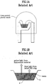
- FIG. 1A illustrates a section of a related art InGaN-YAG white LED
- FIG. 1B illustrates a section showing a detail of the light emitting part in FIG. 1A.
- the related art InGaN-YAG white LEDs in a form of bomb, has a resin layer with a YAG fluorescent material scattered therein inserted in a cap part in a lead frame of an LED.
- a color tone of white light obtainable by changing a ratio of blue/yellow color lights can be achieved by adjusting concentration of YAG fluorescent material mixed with resin.
- FIG. 2 illustrates a graph showing a chromaticity coordinate system, wherein a straight line connecting a chromaticity point of the YAG fluorescent material 1 and a chromaticity point of the InGaN blue LED 2 represents a variable range of a color tone.
- the InGaN-YAG white LED has an InGaN blue LED 2 for emitting a blue color light, and a YAG fluorescent material 1 for emitting a yellowish green color, a combination of the blue color light and the yellowish green color form a white color light.
- the InGaN-YAG white LED since the InGaN-YAG white LED has only one chip, the InGaN-YAG white LED chip requires no control of currents to respective LEDs as in the case a red, green, and blue RGB three color LED. Moreover, the YAG fluorescent material 1 is excited at approx. 460nm, a peak wavelength of the InGaN blue LED 2, has a high transformation efficiency, good water and light resistances, and a low toxicity which is good for environmental protection.
- the YAG fluorescent material 1 is prepared by substituting parts of Y sites and Al sites of Y 3 Al 5 O 12 with Gd and Ga, which is a stable oxide of a garnet structure.
- the transparent YAG fluorescent material 1 absorbs a light from the LED, it has a problem of making a quantum efficiency poor, and reduces yellow components since the YAG fluorescent material 1 has a poor transformation efficiency of approx. 10%.
- an increase of a YAG thickness for increasing the yellow component reduces luminance and quantum efficiencies, further.
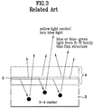
- the ZnSe heteroepitaxy basis white LED is provided with a single crystal n-type ZnSe substrate 3 having I, Cl, Br, Al, Ga, or In added thereto as an S-A (Self-Absorption) center, and a II-VI family LED 4 having a thin film structured p-n junction for emitting white or intermediate color, inclusive of an active layer 5 of ZnSe, ZnCdSe, ZnSeTe, or the like.
- the active layer 5 emits a blue or bluish green light
- an S-A emission center in the ZnSe substrate 3 transforms the blue or bluish green light from the active layer 5 into a yellow or orange light.
- the blue or bluish green light from the active layer 5 and the yellow or orange light from the ZnSe substrate 3 compose an intermediate or white light between a red light and a blue light. That is, the ZnSe white LED generates, not only white light, but also intermediate color lights present between a red light and a blue light, i.e., a redpurple and pink.
- the ZnSe white LED has drawbacks of a high production cost coming from use of an expensive ZnSe substrate, difficulty in adjustment of yellow color intensity from the substrate only by doping of the ZnSe substrate, and difficulty in tuning white color by using the same quantity of injection of current.
- the three color (red, green, and blue) LED basis white LED has AlGaAs, GaAsP for emitting a red light, GaP for emitting a greenish yellow light, SiC and InGaN for emitting a blue light, and AlGaInP for emitting an orange-yellow light, and the like.
- the three color (red, green, and blue) LED basis white LED has problems in that the three color hybrid LED is expensive, a complicated circuit for supplying power to respective chips and a complicated driving circuit are required for producing a white color good for illumination or background light, and an assembled final product has a large size.
- the present invention is directed to a white LED and a method for fabricating the same that addresses one or more of the problems due to limitations and disadvantages of the related art.
- a white LED including a substrate, a first light emission part of III-V family compound semiconductor on the substrate for emission of a light, a second light emission part of II-VI family compound semiconductor on the first light emission part for emission of a light, and electrodes in regions of the substrate, and the first and second light emission parts.
- the first and second light emission parts have a GaAs contact layers respectively
- the substrate is formed of a material selected from a GaAs group or a ZnSe group.
- the first light emission part includes multi-quantum well structure of GaAs/AlGaAs group, or InGaP/AlInGaP group
- the second light emission part includes multi-quantum well structure of ZnCdSe/ZnMgSSe group or ZnCdSe/ZnMgBeSe.
- a white LED including a GaAs substrate, a first light emission part of multi-quantum well structure of GaAs/AlGaAs or InGaP/AlInGaP on the GaAs substrate having a stack of a first clad layer, a first active layer, and a second clad layer disposed in succession, a GaAs first contact layer on the first light emission part, a second light emission part of multi-quantum well structure of ZnCdSe/ZnMgSSe or ZnCdSe/ZnMgBeSe on the GaAs contact layer having a stack of a third clad layer, a second active layer, and a fourth clad layer disposed in succession, a GaAs second contact layer on the second light emission part, and electrodes under the substrate, and regions of the first and second contact parts.
- the substrate and the first contact layer are of different conduction types, and the substrate and the second contact layer are of the same
- a white LED including a GaAs substrate, a first light emission part of multi-quantum well structure of GaAs/AlGaAs or InGaP/AlInGaP on the GaAs substrate having a stack of a first clad layer, a first active layer, and a second clad layer disposed in succession, a GaAs first contact layer on the first light emission part, a second light emission part of multi-quantum well structure of ZnCdSe/ZnMgSSe or ZnCdSe/ZnMgBeSe on the GaAs contact layer having a stack of a third clad layer, a second active layer, and a fourth clad layer disposed in succession, a GaAs second contact layer on the second light emission part, a first electrode under the substrate, a plurality of second electrodes on the first contact layer, a plurality of third electrodes on the second contact layer, and grooves between the second electrodes and between the
- a method for fabricating a white LED including the steps of (a) forming a first light emission part of multi-quantum well structure of GaAs/AlGaAs or InGaP/AlInGaP on a GaAs substrate, and a GaAs first contact layer on the first light emission part, (b) forming a second light emission part of multi-quantum well structure of ZnCdSe/ZnMgSSe or ZnCdSe/ZnMgBeSe on the GaAs contact layer, and a GaAs second contact layer on the second light emission part, (c) etching a portion of the GaAs contact layer and the multi-quantum well structure of ZnCdSe/ZnMgSSe or ZnCdSe/ZnMgBeSe under the GaAs contact layer, for exposing the GaAs first contact layer, and (d) forming electrodes under the substrate and regions of the first and second contact layers
- the method for fabricating a white LED further includes the step of etching the exposed GaAs first, and second contact layers and a region under the first, and second layers to a depth, to form grooves, after the step (c).
- the first light emission part is formed by MOCVD (Metal Organic Chemical Vapor Deposition), or MBE (Molecular Beam Epitaxy)
- the second light emission part is formed by MOCVD (Metal Organic Chemical Vapor Deposition), or MBE (Molecular Beam Epitaxy).
- This document suggests growth of thin films of two different material groups (GaAs group III-V family and ZnSe group II-VI family) on one substrate, to form an LED of two wavelengths, for mixing respective lights from emission layers, to provide a white light or a variety of mixed color lights.
- This document also suggests to combine MOCVD (Metal Organic Chemical Vapor Deposition) or MBE (Molecular Beam Epitaxy), technologies for growing a III-V family compound semiconductor, and the MBE or MOMBE (Metal Organic Molecular Beam Epitaxy), technologies for growing a II-VI family compound semiconductor, on one substrate, to obtain a white or a variety of mixed color LEDs.
- S( ⁇ ) denotes a relative spectrum distribution of a light
- x( ⁇ ), y( ⁇ ), and z( ⁇ ) denote isochromatic functions occurred in the XYZ
- k denotes a constant
- Chromaticity coordinates x, y, and z can be obtained by using the following equation (2) from X, Y, and Z obtained by equation (1). Equation 2.
- x X/(X+Y+Z)
- y Y/(X+Y+Z)
- z Z/(X+Y+Z)
- the equation (2) facilitates selection of means in obtaining the white color light, either by a combination of a plurality of LEDs, or by an LED and other materials.
- the white color light can be obtained, not only from a mixture of the three colors of light, but also a combination of two color lights having appropriate wavelengths as shown in FIG. 2.
- the MBE growth method is mostly used in fabrication of a blue-bluish green LED.
- the present invention suggests employing a GaAs substrate that has a small lattice mismatch of 0.27% to the ZnSe.
- the III-V family and II-VI family compound semiconductor can be grown on the GaAs substrate, with a perfect lattice match made between them, which is understandable from a diagram of a band gap and lattice constant relation of the III-V family and II-VI family compound semiconductor in FIG. 4.
- the AlGaAs or InGaAlP used as III-V family red LED can make a lattice match with the GaAs substrate, as well as with ZnMgBeSe or ZnMgSSe used as II-VI family bluish green LED, which can prevent occurrence of defects caused by a lattice mismatch between the GaAs substrate and the thin film.
- the GaAs basis III-V family compound semiconductor may be used as a material for fabricating an LED of 635 ⁇ 780 nm visible wavelength range
- the II-VI family compound semiconductor may be used as a material for fabricating an LED of 450 ⁇ 550 nm visible wavelength range.
- the III-V family and II-VI family compound semiconductor facilitates an appropriate wavelength adjustment in the neighborhood of red and blue light region, bluish green and green light region, and to compose a mixed color light, such as white, red purple, or pink, by an appropriate wavelength selection.
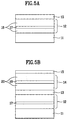
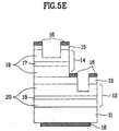
- FIGS. 5A ⁇ 5E illustrate sections showing the steps of a method for fabricating a white LED in accordance with a preferred embodiment of the present invention.
- a quantum well structured AlGaAs/GaAs/AlGaAs, InGaAlP/InGaP/InGaAlP, or the like, the III-V family compound semiconductor 12, is grown primarily on p-GaAs substrate 11 by MOCVD or MBE.
- the AlGaAs or InGaAlP is a cladding layer 18, and GaAs or InGa P is an active layer 17.
- an LED for emitting a red light of a specific wavelength can be fabricated.
- a metal contact layer 13 of n-GaAs is formed on the cladding layer 18.
- the grown metal contact layer 13 of n-GaAs serves as an n-contact for both of the III-V family red LED and the II-VI family blur or bluish green LED in common, and is an initial boundary of the II-VI family compound semiconductor.
- the ZnMgSSe or ZnMgBeSe is a cladding layer 20, and the ZnCdSe is an active layer 19.
- the ZnMgSSe/ZnCdSe/ZnMgSSe, or ZnMgBeSe/ZnCdSe/ZnMgBeSe, a II-VI family compound semiconductor 14, is grown at a low temperature of approx. 250 ⁇ 350°C.
- the III-V family compound semiconductor 12 is primarily grown by MOCVD or MBE, and the II-VI family compound semiconductor 14 is secondarily grown by MBE or MOMBE, for preventing deterioration of device performance caused by collapse of a boundary and inter-diffusion by setting a secondary growth temperature lower than a primary growth temperature.
- MOCVD or MBE the primary growth of the GaAs group III-V family compound semiconductor 12 by MOCVD or MBE is done at the high temperature 650 ⁇ 750°
- the secondary growth of the II-VI family compound semiconductor 14 by MBE or MOMBE is done at a low temperature 250 ⁇ 350°C.
- a surface treatment for preparation of the secondary growth differs depending on the primary growth method of MOCVD or MBE. That is, if the primary growth is by MOCVD, an oxide film is formed on a surface of the semiconductor layer as the primary grown semiconductor layer is exposed to air. Therefore, in order to remove the oxide film from the surface of the semiconductor layer, the surface of the semiconductor layer is required to be subjected to chemical etching and heat treatment in an MBE chamber. Then, by growing an n-GaAs buffer layer 13 in the MBE chamber, possible defects between the III-V family and II-VI family compound semiconductor 12 and 14 thin films can be suppressed to the maximum. If the primary growth is by MBE, since the substrate is transferred to a II-VI family chamber under a high vacuum for secondary growth after the III-V family compound semiconductor 12 thin film is grown, the growth can be started directly without any special surface treatment.
- the II-VI family compound semiconductor 14 is removed completely for exposing the n-GaAs 13 layer by photolithography and chemical or dry etching.
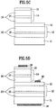
- p-metal electrodes 16 are formed on regions of the p-contact layer 15 of the II-VI compound semiconductor 14 and the p-GaAs substrate 11 respectively, and an n-metal electrode 16 is formed on a region of the n-GaAs 13 layer, a contact layer of the III-V family compound semiconductor 12.
- One in FIG. 5D is an edge emission type LED
- one in FIG. 5E is a surface emission type LED.
- the surface emission type LED is etched down to upper parts of the cladding layers 19 and 20 of the III-V family and the II-VI family compound semiconductors 12 and 14 and regions of the active layers 17 and 18 in fabrication of the white LED for enhancing a luminance.
- FIG. 6 illustrates a diagram showing a result of a low temperature PL spectrum of the white LED of the present invention, wherein Cd composition in Zn x Cd 1-x Se layer used as a quantum well in a II-VI family structure versus wavelength is shown.
- a leakage current may be limited.
- the white LED and the method for fabricating the same have the following advantages.
- III-V family compound semiconductor which has a wavelength of 635 ⁇ 780nm
- II-VI family compound semiconductor which has a wavelength of 450 ⁇ 550nm on a GaAs substrate, with lattices of the two kinds of semiconductor matched, permits to fabricate a white LED which allows a long lifetime and to provide white and a variety of visible lights.
- the III-V family compound semiconductor 12 is primarily grown by MOCVD or MBE at a high temperature, and the II-VI family compound semiconductor 14 is secondarily grown by MBE or MOMBE at a low temperature, for preventing deterioration of device performance caused by collapse of a boundary and inter-diffusion.
- the white LED can be fabricated by using semiconductor laser process technology, no new process technology is required, and by varying currents to the two LEDs only, a visiable light can be varied.
Landscapes
- Led Devices (AREA)
- Physical Deposition Of Substances That Are Components Of Semiconductor Devices (AREA)
Abstract
Description
Preferably, the first and second light emission parts have a GaAs contact layers respectively, and the substrate is formed of a material selected from a GaAs group or a ZnSe group.
Preferably, the first light emission part includes multi-quantum well structure of GaAs/AlGaAs group, or InGaP/AlInGaP group, and the second light emission part includes multi-quantum well structure of ZnCdSe/ZnMgSSe group or ZnCdSe/ZnMgBeSe.
Preferably, the substrate and the first contact layer are of different conduction types, and the substrate and the second contact layer are of the same conduction type.
Preferably, the method for fabricating a white LED further includes the step of etching the exposed GaAs first, and second contact layers and a region under the first, and second layers to a depth, to form grooves, after the step (c).
Preferably, the first light emission part is formed by MOCVD (Metal Organic Chemical Vapor Deposition), or MBE (Molecular Beam Epitaxy), and the second light emission part is formed by MOCVD (Metal Organic Chemical Vapor Deposition), or MBE (Molecular Beam Epitaxy).
In the drawings:
and,

Claims (20)
- A white LED comprising:a substrate;a first light emission part of III-V family compound semiconductor on the substrate for emission of a light;a second light emission part of II-VI family compound semiconductor on the first light emission part for emission of a light; and,electrodes in regions of the substrate, and the first and second light emission parts.
- A white LED as claimed in claim 1, further comprising a metal contact layer on each of the first and second light emission parts.
- A white LED as claimed in claim 2, wherein the metal contact layer is of a GaAs group.
- A white LED as claimed in claim 1, wherein the first light emission part includes multi-quantum well structure of GaAs/AlGaAs group, or InGaP/AlInGaP group.
- A white LED as claimed in claim 1, wherein the second light emission part includes multi-quantum well structure of ZnCdSe/ZnMgSSe group or ZnCdSe/ZnMgBeSe.
- A white LED as claimed in claim 1, wherein the electrodes includes;a first electrode under the substrate,a second electrode on the first light emission part, anda third electrode on the second light emission part.
- A white LED as claimed in claim 1, wherein the electrodes includes;a first electrode under the substrate,a plurality of second electrodes formed on the first light emission part at fixed intervals, anda plurality of third electrodes formed on the second light emission part at fixed intervals, wherein a fixed width groove is formed between adjacent second electrodes and the adjacent third electrodes, to isolate the electrodes.
- A white LED as claimed in claim 7, wherein the groove has a depth not to expose light emission areas of the first and second light emission parts.
- A white LED as claimed in claim 1, wherein the substrate is formed of a material selected from GaAs group or ZnSe group.
- A white LED as claimed in claim 1, wherein the first and second light emission parts emit lights of wavelengths different from each other.
- A white LED comprising:a GaAs substrate;a first light emission part of multi-quantum well structure of GaAs/AlGaAs or InGaP/AlInGaP on the GaAs substrate having a stack of a first clad layer, a first active layer, and a second clad layer disposed in succession;a GaAs first contact layer on the first light emission part;a second light emission part of multi-quantum well structure of ZnCdSe/ZnMgSSe or ZnCdSe/ZnMgBeSe on the GaAs contact layer having a stack of a third clad layer, a second active layer, and a fourth clad layer disposed in succession;a GaAs second contact layer on the second light emission part; and,electrodes under the substrate, and regions of the first and second contact parts.
- A white LED as claimed in claim 11, wherein the substrate and the first contact layer are of different conduction types, and the substrate and the second contact layer are of the same conduction type.
- A white LED comprising:a GaAs substrate;a first light emission part of multi-quantum well structure of GaAs/AlGaAs or InGaP/AlInGaP on the GaAs substrate having a stack of a first clad layer, a first active layer, and a second clad layer disposed in succession;a GaAs first contact layer on the first light emission part;a second light emission part of multi-quantum well structure of ZnCdSe/ZnMgSSe or ZnCdSe/ZnMgBeSe on the GaAs contact layer having a stack of a third clad layer, a second active layer, and a fourth clad layer disposed in succession;a GaAs second contact layer on the second light emission part;a first electrode under the substrate;a plurality of second electrodes on the first contact layer;a plurality of third electrodes on the second contact layer; and,grooves between the second electrodes and between the third electrodes each having a depth for isolating one another.
- A white LED as claimed in claim 13, wherein the substrate and the first contact layer are of different conduction types, and the substrate and the second contact layer are of the same conduction type.
- A white LED as claimed in claim 13, wherein the groove has a depth not to expose active layers of the first and second light emission parts.
- A method for fabricating a white LED, comprising the steps of:(a) forming a first light emission part of multi-quantum well structure of GaAs/AlGaAs or InGaP/AlInGaP on a GaAs substrate, and a GaAs first contact layer on the first light emission part;(b) forming a second light emission part of multi-quantum well structure of ZnCdSe/ZnMgSSe or ZnCdSe/ZnMgBeSe on the GaAs contact layer, and a GaAs second contact layer on the second light emission part;(c) etching a portion of the GaAs contact layer and the multi-quantum well structure of ZnCdSe/ZnMgSSe or ZnCdSe/ZnMgBeSe under the GaAs contact layer, for exposing the GaAs first contact layer; and,(d) forming electrodes under the substrate and regions of the first and second contact layers.
- A method as claimed in claim 16, further comprising the step of etching the exposed GaAs first, and second contact layers and a region under the first, and second layers to a depth, to form grooves, after the step (c).
- A method as claimed in claim 16, wherein the substrate and the first contact layer are of different conduction types, and the substrate and the second contact layer are of the same conduction type.
- A method as claimed in claim 16, wherein the first light emission part is formed by MOCVD (Metal Organic Chemical Vapor Deposition), or MBE (Molecular Beam Epitaxy).
- A method as claimed in claim 16, wherein the second light emission part is formed by MOCVD (Metal Organic Chemical Vapor Deposition), or MBE (Molecular Beam Epitaxy).
Applications Claiming Priority (2)
| Application Number | Priority Date | Filing Date | Title |
|---|---|---|---|
| KR2000031643 | 2000-06-09 | ||
| KR10-2000-0031643A KR100382481B1 (en) | 2000-06-09 | 2000-06-09 | White Light Emitting Diode and Fabricating Method for the same |
Publications (2)
| Publication Number | Publication Date |
|---|---|
| EP1162670A2 true EP1162670A2 (en) | 2001-12-12 |
| EP1162670A3 EP1162670A3 (en) | 2006-06-07 |
Family
ID=19671495
Family Applications (1)
| Application Number | Title | Priority Date | Filing Date |
|---|---|---|---|
| EP01305058A Withdrawn EP1162670A3 (en) | 2000-06-09 | 2001-06-11 | White light emitting diode and method for fabricating the same |
Country Status (4)
| Country | Link |
|---|---|
| US (1) | US20020041148A1 (en) |
| EP (1) | EP1162670A3 (en) |
| JP (1) | JP2002043624A (en) |
| KR (1) | KR100382481B1 (en) |
Cited By (3)
| Publication number | Priority date | Publication date | Assignee | Title |
|---|---|---|---|---|
| EP2159780A2 (en) | 2008-08-29 | 2010-03-03 | Oki Data Corporation | Display device |
| US8076847B2 (en) | 2002-03-22 | 2011-12-13 | Nichia Corporation | Nitride phosphor and production process thereof, and light emitting device |
| CN104953012A (en) * | 2015-06-29 | 2015-09-30 | 广东德力光电有限公司 | AC-LED (alternating current-light emitting diode) chip and application thereof |
Families Citing this family (40)
| Publication number | Priority date | Publication date | Assignee | Title |
|---|---|---|---|---|
| JP4197814B2 (en) * | 1999-11-12 | 2008-12-17 | シャープ株式会社 | LED driving method, LED device and display device |
| JP4055503B2 (en) | 2001-07-24 | 2008-03-05 | 日亜化学工業株式会社 | Semiconductor light emitting device |
| KR20030078122A (en) * | 2002-03-28 | 2003-10-08 | 대주전자재료 주식회사 | Yag-based yellow phosphor comprising lithium and method for the preparation thereof |
| KR100543696B1 (en) * | 2002-09-09 | 2006-01-20 | 삼성전기주식회사 | High efficiency light emitting diode |
| TW586246B (en) * | 2002-10-28 | 2004-05-01 | Super Nova Optoelectronics Cor | Manufacturing method of white light LED and the light-emitting device thereof |
| JP2004153136A (en) * | 2002-10-31 | 2004-05-27 | Sharp Corp | Semiconductor laser device and method of manufacturing the same |
| KR100459495B1 (en) * | 2002-11-08 | 2004-12-03 | 엘지전자 주식회사 | Compound semiconductor light emitting diode |
| TW591811B (en) * | 2003-01-02 | 2004-06-11 | Epitech Technology Corp Ltd | Color mixing light emitting diode |
| CN100379037C (en) * | 2004-01-06 | 2008-04-02 | 晶元光电股份有限公司 | LED structure |
| US7592192B2 (en) | 2004-03-05 | 2009-09-22 | Konica Minolta Holdings, Inc. | White light emitting diode (white LED) and method of manufacturing white LED |
| US7402831B2 (en) * | 2004-12-09 | 2008-07-22 | 3M Innovative Properties Company | Adapting short-wavelength LED's for polychromatic, broadband, or “white” emission |
| US7745814B2 (en) * | 2004-12-09 | 2010-06-29 | 3M Innovative Properties Company | Polychromatic LED's and related semiconductor devices |
| US7719015B2 (en) | 2004-12-09 | 2010-05-18 | 3M Innovative Properties Company | Type II broadband or polychromatic LED's |
| CA2542570A1 (en) * | 2005-04-13 | 2006-10-13 | Black & Decker Inc. | Chop saw |
| WO2007037617A1 (en) * | 2005-09-30 | 2007-04-05 | Seoul Opto Device Co., Ltd. | Light emitting device having vertically stacked light emitting diodes |
| CN100485979C (en) * | 2005-10-17 | 2009-05-06 | 鸿富锦精密工业(深圳)有限公司 | Luminous element, plane illuminant and direct-light-type backlight module |
| DE102006039369A1 (en) * | 2005-12-30 | 2007-07-05 | Osram Opto Semiconductors Gmbh | LED semiconductor for e.g. multiple coach lighting, has two radiation-generating active layers, arranged one above another in vertical direction |
| FR2898434B1 (en) * | 2006-03-13 | 2008-05-23 | Centre Nat Rech Scient | MONOLITHIC WHITE ELECTROLUMINESCENT DIODE |
| US7952110B2 (en) * | 2006-06-12 | 2011-05-31 | 3M Innovative Properties Company | LED device with re-emitting semiconductor construction and converging optical element |
| JP2009540616A (en) * | 2006-06-12 | 2009-11-19 | スリーエム イノベイティブ プロパティズ カンパニー | LED device having re-emitting semiconductor structure and focusing optical element |
| US7863634B2 (en) * | 2006-06-12 | 2011-01-04 | 3M Innovative Properties Company | LED device with re-emitting semiconductor construction and reflector |
| US20070284565A1 (en) * | 2006-06-12 | 2007-12-13 | 3M Innovative Properties Company | Led device with re-emitting semiconductor construction and optical element |
| US7902542B2 (en) | 2006-06-14 | 2011-03-08 | 3M Innovative Properties Company | Adapted LED device with re-emitting semiconductor construction |
| KR101393745B1 (en) * | 2007-06-21 | 2014-05-12 | 엘지이노텍 주식회사 | Semiconductor LED and fabrication method thereof |
| GB2451884A (en) * | 2007-08-16 | 2009-02-18 | Sharp Kk | A Semiconductor Device and a Method of Manufacture Thereof |
| KR20100096173A (en) * | 2007-11-28 | 2010-09-01 | 유니버시티 오브 플로리다 리서치 파운데이션, 인크. | Solarturf: solar energy harvesting artificial turf |
| JP2009137776A (en) * | 2007-12-04 | 2009-06-25 | Sumitomo Electric Ind Ltd | GaAs semiconductor substrate and manufacturing method thereof, and III-V compound semiconductor device and manufacturing method thereof |
| CN101971369B (en) * | 2008-03-14 | 2012-05-23 | 松下电器产业株式会社 | Compound semiconductor light-emitting element, lighting device using the compound semiconductor light-emitting element, and method for manufacturing the compound semiconductor light-emitting element |
| TWI416757B (en) * | 2008-10-13 | 2013-11-21 | 榮創能源科技股份有限公司 | Multi-wavelength light-emitting diode and manufacturing method thereof |
| WO2010044584A2 (en) * | 2008-10-13 | 2010-04-22 | Choi Woon Yong | Led assembly having redundancy electrode and fabrication method thereof |
| JP2011134854A (en) * | 2009-12-24 | 2011-07-07 | Kyocera Corp | Light-emitting element, as well as, optical module and image device equipped with the same |
| JP2012209451A (en) * | 2011-03-30 | 2012-10-25 | Dowa Holdings Co Ltd | Semiconductor light emitting element |
| KR101392977B1 (en) | 2011-09-01 | 2014-05-08 | 에피스타 코포레이션 | A light-emitting element with multiple light-emitting stacked layers |
| JP2016062911A (en) | 2014-09-12 | 2016-04-25 | 株式会社東芝 | Semiconductor light emitting device |
| KR101733225B1 (en) | 2015-04-23 | 2017-05-08 | 광주과학기술원 | Method for integrating different kind of light emitting structure |
| US10868213B2 (en) * | 2018-06-26 | 2020-12-15 | Lumileds Llc | LED utilizing internal color conversion with light extraction enhancements |
| KR102784888B1 (en) * | 2019-12-24 | 2025-03-20 | 엘지디스플레이 주식회사 | Light emitting diode(LED) display device and method for manufacturing LED |
| WO2021134510A1 (en) * | 2019-12-31 | 2021-07-08 | 重庆康佳光电技术研究院有限公司 | Composite dual-wavelength led chip and manufacturing method therefor |
| JP7534427B2 (en) * | 2020-02-10 | 2024-08-14 | グーグル エルエルシー | Display Device and Associated Methods - Patent application |
| CN114497112B (en) * | 2022-03-30 | 2022-07-15 | 季华实验室 | Method for manufacturing a MicroLED display panel and display panel |
Family Cites Families (6)
| Publication number | Priority date | Publication date | Assignee | Title |
|---|---|---|---|---|
| US3343026A (en) * | 1963-11-27 | 1967-09-19 | H P Associates | Semi-conductive radiation source |
| JPH04253381A (en) * | 1991-01-29 | 1992-09-09 | Toshiba Corp | Semiconductor light emitting element and manufacture thereof |
| JPH07263752A (en) * | 1994-03-18 | 1995-10-13 | Sony Corp | Semiconductor color light emitting device |
| JP3543498B2 (en) * | 1996-06-28 | 2004-07-14 | 豊田合成株式会社 | Group III nitride semiconductor light emitting device |
| US5684309A (en) * | 1996-07-11 | 1997-11-04 | North Carolina State University | Stacked quantum well aluminum indium gallium nitride light emitting diodes |
| TW413956B (en) * | 1998-07-28 | 2000-12-01 | Sumitomo Electric Industries | Fluorescent substrate LED |
-
2000
- 2000-06-09 KR KR10-2000-0031643A patent/KR100382481B1/en not_active Expired - Fee Related
-
2001
- 2001-06-08 US US09/876,155 patent/US20020041148A1/en not_active Abandoned
- 2001-06-11 EP EP01305058A patent/EP1162670A3/en not_active Withdrawn
- 2001-06-11 JP JP2001175468A patent/JP2002043624A/en active Pending
Cited By (5)
| Publication number | Priority date | Publication date | Assignee | Title |
|---|---|---|---|---|
| US8076847B2 (en) | 2002-03-22 | 2011-12-13 | Nichia Corporation | Nitride phosphor and production process thereof, and light emitting device |
| EP2159780A2 (en) | 2008-08-29 | 2010-03-03 | Oki Data Corporation | Display device |
| EP2159780A3 (en) * | 2008-08-29 | 2010-11-03 | Oki Data Corporation | Display device |
| US8796703B2 (en) | 2008-08-29 | 2014-08-05 | Oki Data Corporation | Display device capable of emitting light from opposite sides |
| CN104953012A (en) * | 2015-06-29 | 2015-09-30 | 广东德力光电有限公司 | AC-LED (alternating current-light emitting diode) chip and application thereof |
Also Published As
| Publication number | Publication date |
|---|---|
| KR20010110916A (en) | 2001-12-15 |
| EP1162670A3 (en) | 2006-06-07 |
| KR100382481B1 (en) | 2003-05-01 |
| US20020041148A1 (en) | 2002-04-11 |
| JP2002043624A (en) | 2002-02-08 |
Similar Documents
| Publication | Publication Date | Title |
|---|---|---|
| EP1162670A2 (en) | White light emitting diode and method for fabricating the same | |
| US6163038A (en) | White light-emitting diode and method of manufacturing the same | |
| Schlotter et al. | Fabrication and characterization of GaN/InGaN/AlGaN double heterostructure LEDs and their application in luminescence conversion LEDs | |
| US8470618B2 (en) | Method of manufacturing a light-emitting diode having electrically active and passive portions | |
| US6548834B2 (en) | Semiconductor light emitting element | |
| US6590233B2 (en) | Semiconductor light emitting device | |
| US8389975B2 (en) | Group III nitride semiconductor light-emitting device | |
| US7045375B1 (en) | White light emitting device and method of making same | |
| US20090108276A1 (en) | High Efficiency Dilute Nitride Light Emitting Diodes | |
| KR100237804B1 (en) | Semiconductor light emitting device and method for manufacturing same | |
| KR20100059854A (en) | Radiation-emitting semiconductor body | |
| Yamada et al. | A methodological study of the best solution for generating white light using nitride-based light-emitting diodes | |
| JPH0710003B2 (en) | Mixed color light emitting semiconductor device | |
| US20040090779A1 (en) | Light mixing led and manufacturing method thereof | |
| JPH11121806A (en) | Semiconductor light emitting device | |
| JP2875124B2 (en) | Semiconductor light emitting device and method of manufacturing the same | |
| JPH1187773A (en) | Light emitting element | |
| KR100433989B1 (en) | Semiconductor LED device and manufacturing metheod thereof | |
| JP2004165604A (en) | Light emitting diode and method of manufacturing the same | |
| JP2006041077A (en) | Phosphor | |
| KR102399381B1 (en) | Light emitting device | |
| JP2003332619A (en) | Semiconductor light emitting device | |
| KR100459495B1 (en) | Compound semiconductor light emitting diode | |
| Nakamura | InGaN light-emitting diodes with quantum-well structures | |
| JPH10144961A (en) | Semiconductor light emitting device |
Legal Events
| Date | Code | Title | Description |
|---|---|---|---|
| PUAI | Public reference made under article 153(3) epc to a published international application that has entered the european phase |
Free format text: ORIGINAL CODE: 0009012 |
|
| AK | Designated contracting states |
Kind code of ref document: A2 Designated state(s): AT BE CH CY DE DK ES FI FR GB GR IE IT LI LU MC NL PT SE TR |
|
| AX | Request for extension of the european patent |
Free format text: AL;LT;LV;MK;RO;SI |
|
| PUAL | Search report despatched |
Free format text: ORIGINAL CODE: 0009013 |
|
| AK | Designated contracting states |
Kind code of ref document: A3 Designated state(s): AT BE CH CY DE DK ES FI FR GB GR IE IT LI LU MC NL PT SE TR |
|
| AX | Request for extension of the european patent |
Extension state: AL LT LV MK RO SI |
|
| AKX | Designation fees paid | ||
| REG | Reference to a national code |
Ref country code: DE Ref legal event code: 8566 |
|
| STAA | Information on the status of an ep patent application or granted ep patent |
Free format text: STATUS: THE APPLICATION IS DEEMED TO BE WITHDRAWN |
|
| 18D | Application deemed to be withdrawn |
Effective date: 20061208 |