EP1162440B1 - Infrared sensing element and temperature measuring device - Google Patents
Infrared sensing element and temperature measuring device Download PDFInfo
- Publication number
- EP1162440B1 EP1162440B1 EP01304921A EP01304921A EP1162440B1 EP 1162440 B1 EP1162440 B1 EP 1162440B1 EP 01304921 A EP01304921 A EP 01304921A EP 01304921 A EP01304921 A EP 01304921A EP 1162440 B1 EP1162440 B1 EP 1162440B1
- Authority
- EP
- European Patent Office
- Prior art keywords
- infrared
- sensing element
- temperature
- infrared sensing
- junction
- Prior art date
- Legal status (The legal status is an assumption and is not a legal conclusion. Google has not performed a legal analysis and makes no representation as to the accuracy of the status listed.)
- Expired - Lifetime
Links
- 239000000758 substrate Substances 0.000 claims description 81
- 239000004020 conductor Substances 0.000 claims description 69
- 239000004065 semiconductor Substances 0.000 claims description 54
- 239000006096 absorbing agent Substances 0.000 claims description 46
- 230000005855 radiation Effects 0.000 claims description 41
- 238000005530 etching Methods 0.000 claims description 10
- 238000005259 measurement Methods 0.000 description 51
- 239000010409 thin film Substances 0.000 description 46
- 239000010408 film Substances 0.000 description 35
- XUIMIQQOPSSXEZ-UHFFFAOYSA-N Silicon Chemical compound [Si] XUIMIQQOPSSXEZ-UHFFFAOYSA-N 0.000 description 29
- 229910052710 silicon Inorganic materials 0.000 description 29
- 239000010703 silicon Substances 0.000 description 29
- 230000003247 decreasing effect Effects 0.000 description 27
- 238000009529 body temperature measurement Methods 0.000 description 26
- 230000035945 sensitivity Effects 0.000 description 26
- 230000036760 body temperature Effects 0.000 description 17
- 229910021420 polycrystalline silicon Inorganic materials 0.000 description 17
- 229920005591 polysilicon Polymers 0.000 description 17
- 230000007423 decrease Effects 0.000 description 16
- 238000004519 manufacturing process Methods 0.000 description 16
- XAGFODPZIPBFFR-UHFFFAOYSA-N aluminium Chemical compound [Al] XAGFODPZIPBFFR-UHFFFAOYSA-N 0.000 description 15
- 230000008859 change Effects 0.000 description 13
- 229910052782 aluminium Inorganic materials 0.000 description 12
- 239000000463 material Substances 0.000 description 9
- 238000000034 method Methods 0.000 description 8
- 238000012545 processing Methods 0.000 description 8
- 210000003454 tympanic membrane Anatomy 0.000 description 8
- 229910052751 metal Inorganic materials 0.000 description 7
- 239000002184 metal Substances 0.000 description 7
- 230000002093 peripheral effect Effects 0.000 description 7
- 229910052732 germanium Inorganic materials 0.000 description 6
- GNPVGFCGXDBREM-UHFFFAOYSA-N germanium atom Chemical compound [Ge] GNPVGFCGXDBREM-UHFFFAOYSA-N 0.000 description 6
- 239000012535 impurity Substances 0.000 description 6
- 102100031250 Disks large-associated protein 1 Human genes 0.000 description 5
- 102100031245 Disks large-associated protein 2 Human genes 0.000 description 5
- 101150020562 Dlgap2 gene Proteins 0.000 description 5
- 101000731000 Homo sapiens Membrane-associated progesterone receptor component 1 Proteins 0.000 description 5
- 101100062430 Saccharomyces cerevisiae (strain ATCC 204508 / S288c) DAP2 gene Proteins 0.000 description 5
- 239000005083 Zinc sulfide Substances 0.000 description 5
- 238000005304 joining Methods 0.000 description 5
- 238000002360 preparation method Methods 0.000 description 5
- 229910052984 zinc sulfide Inorganic materials 0.000 description 5
- 238000010276 construction Methods 0.000 description 4
- 239000012528 membrane Substances 0.000 description 4
- 150000004767 nitrides Chemical class 0.000 description 4
- 230000008569 process Effects 0.000 description 4
- 239000000523 sample Substances 0.000 description 4
- 230000015572 biosynthetic process Effects 0.000 description 3
- 238000005229 chemical vapour deposition Methods 0.000 description 3
- 238000010586 diagram Methods 0.000 description 3
- 230000007613 environmental effect Effects 0.000 description 3
- 230000001747 exhibiting effect Effects 0.000 description 3
- PCHJSUWPFVWCPO-UHFFFAOYSA-N gold Chemical compound [Au] PCHJSUWPFVWCPO-UHFFFAOYSA-N 0.000 description 3
- 239000010931 gold Substances 0.000 description 3
- 229910052737 gold Inorganic materials 0.000 description 3
- DRDVZXDWVBGGMH-UHFFFAOYSA-N zinc;sulfide Chemical compound [S-2].[Zn+2] DRDVZXDWVBGGMH-UHFFFAOYSA-N 0.000 description 3
- 229910052581 Si3N4 Inorganic materials 0.000 description 2
- 229910006367 Si—P Inorganic materials 0.000 description 2
- 230000008901 benefit Effects 0.000 description 2
- 239000000919 ceramic Substances 0.000 description 2
- 239000011248 coating agent Substances 0.000 description 2
- 238000000576 coating method Methods 0.000 description 2
- 238000012937 correction Methods 0.000 description 2
- 238000005520 cutting process Methods 0.000 description 2
- 230000002542 deteriorative effect Effects 0.000 description 2
- 239000000428 dust Substances 0.000 description 2
- 230000008020 evaporation Effects 0.000 description 2
- 238000001704 evaporation Methods 0.000 description 2
- 230000006872 improvement Effects 0.000 description 2
- 238000012986 modification Methods 0.000 description 2
- 230000004048 modification Effects 0.000 description 2
- 238000012856 packing Methods 0.000 description 2
- 239000002245 particle Substances 0.000 description 2
- 230000010287 polarization Effects 0.000 description 2
- 238000000926 separation method Methods 0.000 description 2
- 238000004544 sputter deposition Methods 0.000 description 2
- 238000012360 testing method Methods 0.000 description 2
- OAICVXFJPJFONN-UHFFFAOYSA-N Phosphorus Chemical compound [P] OAICVXFJPJFONN-UHFFFAOYSA-N 0.000 description 1
- 230000005678 Seebeck effect Effects 0.000 description 1
- NRTOMJZYCJJWKI-UHFFFAOYSA-N Titanium nitride Chemical compound [Ti]#N NRTOMJZYCJJWKI-UHFFFAOYSA-N 0.000 description 1
- 238000010521 absorption reaction Methods 0.000 description 1
- 230000005540 biological transmission Effects 0.000 description 1
- YXTPWUNVHCYOSP-UHFFFAOYSA-N bis($l^{2}-silanylidene)molybdenum Chemical compound [Si]=[Mo]=[Si] YXTPWUNVHCYOSP-UHFFFAOYSA-N 0.000 description 1
- 238000000151 deposition Methods 0.000 description 1
- 238000013461 design Methods 0.000 description 1
- 238000001514 detection method Methods 0.000 description 1
- 230000006866 deterioration Effects 0.000 description 1
- 238000009826 distribution Methods 0.000 description 1
- 230000000694 effects Effects 0.000 description 1
- 238000007710 freezing Methods 0.000 description 1
- 238000007429 general method Methods 0.000 description 1
- 238000010438 heat treatment Methods 0.000 description 1
- 230000006698 induction Effects 0.000 description 1
- 150000002500 ions Chemical class 0.000 description 1
- 230000007246 mechanism Effects 0.000 description 1
- 239000007769 metal material Substances 0.000 description 1
- 229910021344 molybdenum silicide Inorganic materials 0.000 description 1
- 230000003287 optical effect Effects 0.000 description 1
- 238000000059 patterning Methods 0.000 description 1
- 229910052698 phosphorus Inorganic materials 0.000 description 1
- 239000011574 phosphorus Substances 0.000 description 1
- 238000000206 photolithography Methods 0.000 description 1
- 230000004043 responsiveness Effects 0.000 description 1
- HQVNEWCFYHHQES-UHFFFAOYSA-N silicon nitride Chemical compound N12[Si]34N5[Si]62N3[Si]51N64 HQVNEWCFYHHQES-UHFFFAOYSA-N 0.000 description 1
- 229910000679 solder Inorganic materials 0.000 description 1
- 230000001052 transient effect Effects 0.000 description 1
- WQJQOUPTWCFRMM-UHFFFAOYSA-N tungsten disilicide Chemical compound [Si]#[W]#[Si] WQJQOUPTWCFRMM-UHFFFAOYSA-N 0.000 description 1
- 229910021342 tungsten silicide Inorganic materials 0.000 description 1
Images


Classifications
-
- G—PHYSICS
- G01—MEASURING; TESTING
- G01J—MEASUREMENT OF INTENSITY, VELOCITY, SPECTRAL CONTENT, POLARISATION, PHASE OR PULSE CHARACTERISTICS OF INFRARED, VISIBLE OR ULTRAVIOLET LIGHT; COLORIMETRY; RADIATION PYROMETRY
- G01J5/00—Radiation pyrometry, e.g. infrared or optical thermometry
- G01J5/02—Constructional details
- G01J5/04—Casings
-
- G—PHYSICS
- G01—MEASURING; TESTING
- G01J—MEASUREMENT OF INTENSITY, VELOCITY, SPECTRAL CONTENT, POLARISATION, PHASE OR PULSE CHARACTERISTICS OF INFRARED, VISIBLE OR ULTRAVIOLET LIGHT; COLORIMETRY; RADIATION PYROMETRY
- G01J5/00—Radiation pyrometry, e.g. infrared or optical thermometry
- G01J5/02—Constructional details
- G01J5/021—Probe covers for thermometers, e.g. tympanic thermometers; Containers for probe covers; Disposable probes
-
- G—PHYSICS
- G01—MEASURING; TESTING
- G01J—MEASUREMENT OF INTENSITY, VELOCITY, SPECTRAL CONTENT, POLARISATION, PHASE OR PULSE CHARACTERISTICS OF INFRARED, VISIBLE OR ULTRAVIOLET LIGHT; COLORIMETRY; RADIATION PYROMETRY
- G01J5/00—Radiation pyrometry, e.g. infrared or optical thermometry
- G01J5/02—Constructional details
- G01J5/0225—Shape of the cavity itself or of elements contained in or suspended over the cavity
-
- G—PHYSICS
- G01—MEASURING; TESTING
- G01J—MEASUREMENT OF INTENSITY, VELOCITY, SPECTRAL CONTENT, POLARISATION, PHASE OR PULSE CHARACTERISTICS OF INFRARED, VISIBLE OR ULTRAVIOLET LIGHT; COLORIMETRY; RADIATION PYROMETRY
- G01J5/00—Radiation pyrometry, e.g. infrared or optical thermometry
- G01J5/02—Constructional details
- G01J5/04—Casings
- G01J5/041—Mountings in enclosures or in a particular environment
- G01J5/045—Sealings; Vacuum enclosures; Encapsulated packages; Wafer bonding structures; Getter arrangements
-
- G—PHYSICS
- G01—MEASURING; TESTING
- G01J—MEASUREMENT OF INTENSITY, VELOCITY, SPECTRAL CONTENT, POLARISATION, PHASE OR PULSE CHARACTERISTICS OF INFRARED, VISIBLE OR ULTRAVIOLET LIGHT; COLORIMETRY; RADIATION PYROMETRY
- G01J5/00—Radiation pyrometry, e.g. infrared or optical thermometry
- G01J5/02—Constructional details
- G01J5/04—Casings
- G01J5/048—Protective parts
-
- G—PHYSICS
- G01—MEASURING; TESTING
- G01J—MEASUREMENT OF INTENSITY, VELOCITY, SPECTRAL CONTENT, POLARISATION, PHASE OR PULSE CHARACTERISTICS OF INFRARED, VISIBLE OR ULTRAVIOLET LIGHT; COLORIMETRY; RADIATION PYROMETRY
- G01J5/00—Radiation pyrometry, e.g. infrared or optical thermometry
- G01J5/02—Constructional details
- G01J5/04—Casings
- G01J5/049—Casings for tympanic thermometers
-
- G—PHYSICS
- G01—MEASURING; TESTING
- G01J—MEASUREMENT OF INTENSITY, VELOCITY, SPECTRAL CONTENT, POLARISATION, PHASE OR PULSE CHARACTERISTICS OF INFRARED, VISIBLE OR ULTRAVIOLET LIGHT; COLORIMETRY; RADIATION PYROMETRY
- G01J5/00—Radiation pyrometry, e.g. infrared or optical thermometry
- G01J5/02—Constructional details
- G01J5/05—Means for preventing contamination of the components of the optical system; Means for preventing obstruction of the radiation path
-
- G—PHYSICS
- G01—MEASURING; TESTING
- G01J—MEASUREMENT OF INTENSITY, VELOCITY, SPECTRAL CONTENT, POLARISATION, PHASE OR PULSE CHARACTERISTICS OF INFRARED, VISIBLE OR ULTRAVIOLET LIGHT; COLORIMETRY; RADIATION PYROMETRY
- G01J5/00—Radiation pyrometry, e.g. infrared or optical thermometry
- G01J5/02—Constructional details
- G01J5/08—Optical arrangements
- G01J5/0801—Means for wavelength selection or discrimination
-
- G—PHYSICS
- G01—MEASURING; TESTING
- G01J—MEASUREMENT OF INTENSITY, VELOCITY, SPECTRAL CONTENT, POLARISATION, PHASE OR PULSE CHARACTERISTICS OF INFRARED, VISIBLE OR ULTRAVIOLET LIGHT; COLORIMETRY; RADIATION PYROMETRY
- G01J5/00—Radiation pyrometry, e.g. infrared or optical thermometry
- G01J5/02—Constructional details
- G01J5/08—Optical arrangements
- G01J5/0806—Focusing or collimating elements, e.g. lenses or concave mirrors
-
- G—PHYSICS
- G01—MEASURING; TESTING
- G01J—MEASUREMENT OF INTENSITY, VELOCITY, SPECTRAL CONTENT, POLARISATION, PHASE OR PULSE CHARACTERISTICS OF INFRARED, VISIBLE OR ULTRAVIOLET LIGHT; COLORIMETRY; RADIATION PYROMETRY
- G01J5/00—Radiation pyrometry, e.g. infrared or optical thermometry
- G01J5/02—Constructional details
- G01J5/08—Optical arrangements
- G01J5/0818—Waveguides
-
- G—PHYSICS
- G01—MEASURING; TESTING
- G01J—MEASUREMENT OF INTENSITY, VELOCITY, SPECTRAL CONTENT, POLARISATION, PHASE OR PULSE CHARACTERISTICS OF INFRARED, VISIBLE OR ULTRAVIOLET LIGHT; COLORIMETRY; RADIATION PYROMETRY
- G01J5/00—Radiation pyrometry, e.g. infrared or optical thermometry
- G01J5/10—Radiation pyrometry, e.g. infrared or optical thermometry using electric radiation detectors
- G01J5/12—Radiation pyrometry, e.g. infrared or optical thermometry using electric radiation detectors using thermoelectric elements, e.g. thermocouples
- G01J5/14—Electrical features thereof
- G01J5/16—Arrangements with respect to the cold junction; Compensating influence of ambient temperature or other variables
-
- G—PHYSICS
- G01—MEASURING; TESTING
- G01J—MEASUREMENT OF INTENSITY, VELOCITY, SPECTRAL CONTENT, POLARISATION, PHASE OR PULSE CHARACTERISTICS OF INFRARED, VISIBLE OR ULTRAVIOLET LIGHT; COLORIMETRY; RADIATION PYROMETRY
- G01J5/00—Radiation pyrometry, e.g. infrared or optical thermometry
- G01J5/70—Passive compensation of pyrometer measurements, e.g. using ambient temperature sensing or sensing of temperature within housing
-
- G—PHYSICS
- G01—MEASURING; TESTING
- G01J—MEASUREMENT OF INTENSITY, VELOCITY, SPECTRAL CONTENT, POLARISATION, PHASE OR PULSE CHARACTERISTICS OF INFRARED, VISIBLE OR ULTRAVIOLET LIGHT; COLORIMETRY; RADIATION PYROMETRY
- G01J5/00—Radiation pyrometry, e.g. infrared or optical thermometry
- G01J5/02—Constructional details
- G01J5/06—Arrangements for eliminating effects of disturbing radiation; Arrangements for compensating changes in sensitivity
- G01J5/064—Ambient temperature sensor; Housing temperature sensor; Constructional details thereof
Definitions
- the present invention relates to a thermopile infrared sensing element and a temperature measuring device using the same.
- a known temperature measuring device uses an infrared sensing element which detects infrared radiation emitted from a heat source and converts it into an electric signal.
- infrared sensing elements include a thermopile type, a pyroelectric type, a bolometer and the like.
- the thermopile infrared sensing element utilizes the Seebeck effect of a thermopile comprising a thermocouple or a plurality of themlocouples connected in series, for detecting a temperature change due to infrared radiation or absorption as thermoelectromotive force.
- the pyroelectric infrared sensing element detects a temperature by using a change in floating charge due to polarization according to the infrared thermal energy, i.e., a pyroelectric effect, of a base material comprising ceramic or the like.
- the borometer comprises a thermosensitive resistor comprising a thin film or a thin wire of a metal or the like so that a thermal change in resistance value of the resistor is detected.
- the pyroelectric infrared sensing element requires a shutter provided on an optical path, for alternately measuring the temperatures of a surface to be measured and a reference point because polarization occurs only at the moment of application of thermal energy. Therefore, it is difficult to miniaturize the pyroelectric infrared sensing element and improve measurement accuracy.
- the pyroelectric infrared sensing element can thus be used for applications such as a "body sensing element" of an automatic door and the like, which are not usually required to have a small size or high measurement accuracy.
- the pyroelectric infrared sensing element is unsuitable for a temperature measuring device such as a clinical thermometer or the like, which is required to measure temperatures with high accuracy and have a small size and low cost.
- the pyroelectric and thermopile infrared sensing elements require detecting a relative temperature difference from a reference temperature, while the borometer has the advantage that an absolute temperature can be measured.
- the borometer has many causes of error, such as self heating due to measuring current, current noise, etc., thereby causing difficulties in improving the measurement accuracy.
- the borometer also requires a bias current to complicate the structure, thereby complicating handling.
- thermopile infrared sensing element does not use such a transient phenomenon as utilized by the pyroelectric type and such excess measuring current as flowing through the borometer, and thus the thermopile infrared sensing element can stably detect or measure temperatures. Furthermore, the thermopile infrared sensing element can be miniaturized by using the semiconductor manufacturing process at low cost, and is thus suitable for a temperature measuring device such as a clinical thermometer or the like, which is required to be small in size and inexpensive.
- Fig. 21 shows an ear-type clinical thermometer 100 as a temperature measuring device using a thermopile infrared sensor or infrared sensing element.
- the ear-type clinical thermometer 100 comprises a body case 11, an infrared receiving sensing unit 200 which receives infrared radiation from the ear to output a voltage signal according to the temperature of the ear, i.e., the temperature of the tympanic membrane, and a circuit board 3 on which various electronic parts and circuits are mounted.
- various electronic parts 4C are mounted to form a temperature deriving circuit 400 for determining the temperature of the tympanic membrane based on the output voltage of the infrared receiving sensing unit 200, or the body temperature based on the temperature of the tympanic membrane. Furthermore, LCD 5 for displaying the determined temperature, and the like, and a power source 6 for supplying electric power to each of the units are also mounted on the circuit board 3.
- the infrared receiving sensing unit 200 comprises a case 211 having a cylindrical shape which projects forward (to the right of the drawing) to permit the front end to be inserted into the lughole, a wave guide 206 contained in the case 211, and an infrared sensing chip 210 arranged at the base of the wave guide 206 to face the front end of the case 211.
- the front end of the case 211 is open, and covered with an infrared transmitting probe cap 25, and the front opening of the wave guide 206 is covered with an infrared transmitting film 23 for preventing entrance of dust particles, etc, the film 23 being supported by a film holding O-ring 24.
- infrared radiation entering the infrared receiving sensing unit 200 is guided to the infrared sensing chip 210 by the wave guide 206 so that the infrared sensing chip 210 receives the infrared radiation corresponding to the temperature of the tympanic membrane to output a voltage signal according to the infrared radiation. Therefore, when a temperature measurement switch SW4 of the ear-type clinical thermometer 100 is pushed, the body temperature can be measured by the infrared receiving sensing unit 200 through infrared radiation.
- the clinical thermometer 100 is a wave guide type in which infrared radiation entering from a heat source (the lughole) S is transmitted through the wave guide 206 arranged in front of the infrared sensing chip 210 to be guided to the infrared sensing chip 210, as shown in Fig. 22.
- the temperature rise due to the infrared radiation is converted into a voltage by the thermopile of the infrared sensing chip 210 and then output.
- Fig. 23 shows the infrared sensing chip 210.
- the infrared sensing chip 210 comprises a thermopile infrared sensor 209, and a thermistor 211, both of which are mounted on a package substrate 212.
- the thermistor 211 is used for determining the reference temperature of the thermopile formed in the infrared sensor 209, i.e., the temperature of the cold junction.
- These components are contained in a package case 213 to unify the components.
- the package case 213 further comprises an infrared filter 208 composed of silicon or the like and provided in a window which infrared radiation enters, for cutting-off visible light and transmitting infrared radiation.
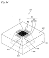
- Fig. 24 is a perspective view schematically showing the infrared sensor or infrared sensing element 209.
- the infrared sensor 209 comprises a base 80 comprising a portion (thin film portion) 802 in which only a thin film is left by etching a silicon substrate to form a hollow at the center of the lower surface or the bottom of the silicon substrate, and a thick wall portion 801 in which the silicon substrate remains unetched.
- the infrared sensor 209 has a structure in which a hollow portion KW is formed at the center of the base 80 from the lower side to form a membrane at the top of the base 80.
- gold black is deposited at the top of the thin film portion 802 by sputtering, evaporation, or the like to form an infrared absorber 81 comprising a black body for absorbing infrared radiation.
- the infrared absorber 81 absorbs infrared radiation to cause a change in temperature.
- the infrared sensor 209 further comprises a plurality of thermocouples 82 with high sensitivity, which are provided on every side of the infrared absorber 81.
- the hot junction 83 of each of the thermocouples 82 is arranged near the infrared absorber 81 or to be overlapped with it, and the cold junction 84 of each thermocouple 82 is arranged in the peripheral thick wall portion 801 in which the silicon substrate remains.
- electromotive force occurs between the hot junction 83 and the cold junction 84 of each thermocouple 82 according to a temperature rise of the infrared absorber 81, the electromotive force produced by a single thermocouple 82 is not sufficient.
- the infrared sensor 209 comprises a plurality of thermocouples 82 which are connected in series to form a thermopile 85 so that a voltage between both ends serving as a terminal (for example, + terminal) 86 and a terminal (for example, - terminal) 87 can be output.
- each of the thermocouples 82 comprises two types of conductors of aluminum (A1) 91 and polysilicon (Si-P) 92.
- the polysilicon 92 is deposited in a line shape.
- the end of each of the polysilicon conductors 92, which is arranged near the infrared absorber 81, i.e., which is arranged in the thin film portion 802, is joined to the aluminum wiring 91 to form the hot junction 83.
- the end of each polysilicon conductor 92 which is arranged in the thick wall portion 801 functioning as a heat sink, is joined to the aluminum wiring 91 to form the cold junction 84.
- Each aluminum wiring 91 connects the hot junction 83 and the cold junction 84 of the adjacent polysilicon conductors 92, resulting in a state where the thermocouples 82 are connected in series.
- Fig. 26 is a block diagram schematically showing the functional configuration of the ear-type clinical thermometer 100.
- the ear-type clinical thermometer 100 comprises the temperature deriving circuit 400 to which a temperature sensing voltage Vt between both terminals 86 and 87 of the thermopile 85 of the infrared sensor 209 is input to output temperature T based on the voltage Vt to the LCD 5.
- the temperature deriving circuit 400 comprises an amplifier 41 for amplifying the temperature sensing voltage Vt, an A/D converter 42 for converting the output from the amplifier 41 to a digital value, CPU 44 for performing numerical processing of the digital value to determine the temperature corresponding to the temperature sensing voltage Vt, and RAM 43 serving as a working area for each processing in the CPU 44.
- the temperature deriving circuit 400 detects the electromotive force produced between the hot junctions 83 and the cold junctions 84 of the thermopile 85 of the infrared sensor 209 according to a change in temperature to determine the temperature difference Ts between the hot junctions 83 and the cold junctions 84 based on the output voltage Vt.
- the temperature of the infrared absorber 81 In order to determine the temperature of the infrared absorber 81 to calculate the body temperature T (herein, the temperature of the tympanic membrane), the temperature (reference temperature) of the cold junctions 84 must be determined for correction.
- the infrared sensing chip 210 contains the thermistor 211 so as to detect the reference temperature Tr of the infrared sensor 209.
- the temperature deriving circuit 400 further comprises an amplifier 45 for amplifying the output current It of the thermistor 211, and an A/D converter 46 for converting the output to a digital value to supply a digital signal to the CPU 44.
- the CPU 44 can thus correct the temperature difference Ts obtained by the signal from the thermopile 85 with the reference temperature Tr obtained by the thermistor 211 to determine the body temperature T.
- the thermistor 211 simply measures the temperature on the side of the infrared sensor 209, i.e., the environmental temperature around the infrared sensor 209 within the infrared detecting chip 210. Therefore, the temperature detected by the thermistor 211 is different from the actual temperature of the cold junctions 84, thereby possibly causing great error in the body temperature T determined as described above.
- the thermistor 211 is apparently suitable for measuring the reference temperature in view of the fact that the absolute temperature can be measured because the resistivity changes with temperature.
- the temperature characteristic is nonlinear, and thus an appropriate compensating circuit is required.
- the range of precise temperature measurement is limited. Therefore, in use of the ear-type clinical thermometer 100, the range of room temperature which permits precise measurement is possibly limited, and thus the body temperature cannot be always easily measured with high accuracy depending upon the environment of measurement.
- an object of the present invention is to provide an infrared sensing element and a temperature measuring device using the same which permit an improvement in accuracy of temperature measurement when the temperature is measured by using the above-described thermopile infrared sensing element.
- Another object of the present invention is to provide an infrared sensing element and a temperature measuring device using the same which permit temperature measurement with ease and high accuracy under any environment.
- EP0999437 discloses a thermometer having an infrared sensor comprising a silicon substrate on which a thermopile is formed.
- the silicon substrate is thicker in peripheral portions than in a central portion and the cold junctions of the thermopile are formed over the peripheral portions.
- a room temperature sensor may be used to measure the temperature of the infrared sensor.
- thermometer having an infrared sensor comprising a thermopile mounted on a ceramic base having a thicker peripheral portion and a thinner central portion.
- a thermocouple having a cold junction positioned on the peripheral portion is used to measure the ambient temperature at which the thermopile is operating.
- an infrared sensing element comprising: a base comprising a film portion and a wall portion provided around the film portion, wherein the wall portion is thicker than the film portion and a base of at least the wall portion is formed from a semiconductor substrate; a thermopile comprising a plurality of thermocouples formed so that cold junctions are located on the wall portion, and hot junctions are located on the film portion; and characterised by reference temperature sensing means comprising a thermosensitive portion in contact with the wall portion, wherein the thermosensitive portion comprises at least one PN junction formed on the semiconductor substrate and a PN junction is formed below each of the cold junctions.
- thermosensitive portion is arranged in contact with the thick wall portion of the base, which serves as a heat sink of the thermopile. Therefore, the temperature of the thick wall portion in contact with the cold junctions of the thermopile can be detected directly by the thermosensitive portion, and thus the temperature of the cold junctions can be detected substantially accurately even when the environment around the infrared sensing element changes.
- a temperature measuring device comprising the infrared sensing element of the present invention, and means for determining temperature from the output voltage of the thermopile based on the reference temperature determined by the reference temperature sensing means is capable of measuring temperature with high accuracy.
- the infrared sensing element of the present invention is a thermopile infrared sensing element, and permits mass-production of small size elements at low cost by utilizing a semiconductor manufacturing process. Therefore, by using the infrared sensing element of the present invention, a compact temperature measuring device can be provided at low cost, which can measure temperature with high accuracy.
- thermosensitive portion for example, a diode
- the base of at least the thick wall portion of the base comprises a semiconductor substrate so that the thermosensitive portion comprises the PN junction formed on the semiconductor substrate.
- an infrared sensing element comprising a compact thermosensitive portion can be formed.
- the thermosensitive portion can be formed by the semiconductor process, thereby decreasing the manufacturing cost.
- the temperature characteristic noalinearly changes, and thus the range of temperature measurement is limited, thereby causing the restriction that the body temperature cannot be accurately measured by a conventional clinical thermometer using a thermistor unless the room temperature is about 15°C or more.
- the infrared sensing element of the present invention comprises the PN junction as the thermosensitive portion, and temperature determining means include means for determining the reference temperature based on the forward voltage drop of the PN junction, whereby a compact temperature measuring device with high measurement accuracy within a wide temperature range can be provided at low cost.
- the infrared sensing element of the present invention comprises a plurality of PN junctions as the thermosensitive portion, and temperature determining means include means for determining the reference temperature based on the difference between the forward voltage drops of the plurality of PN junctions, whereby a temperature measuring device with higher measurement accuracy can be provided.
- the PN junctions may be arranged in any portion of the semiconductor substrate, the PN junctions are preferably arranged in parallel near the semiconductor substrate in order to prevent differences in characteristic between the PN junctions.
- the parallel arrangement of the PN junctions enables the use of a common conductor layer as the conductor layers on one side in the plurality of PN junctions, thereby improving the space efficiency and decreasing the number of electrodes. Therefore, the infrared sensing element of the present invention can be further decreased in size.
- a single anode region, and a plurality of cathode regions extending in parallel to the anode region can be provided.
- the PN junction is formed below each of the cold junctions to bring the thermosensitive portion nearer to the cold junction, whereby the reference temperature can be more correctly detected. It is thus possible to further improve the accuracy of temperature measurement.
- a plurality of PN junctions having a plurality of cold junctions arranged to form the thermopile are formed along the periphery of the thin film portion, the average reference temperature of the cold junctions can be obtained, thereby obtaining the more accurate reference temperature and improving the accuracy of temperature measurement.
- electrodes are preferably respectively formed on the upper surfaces of first and second conductor layers of the PN junction so as to extend along the first and second conductor layers, thereby decreasing a potential difference in the same conductor as much as possible.
- a second substrate may be provided on the thick wall portion of the base to be joined to the thick wall portion, and the thermosensitive portion may be provided on the base and/or the second substrate at the junction between the base and the second substrate.
- the second substrate comprises an infrared lens or wave guide
- the temperature of the infrared lens or wave guide can be obtained at the same time as detection of the reference temperature. Therefore, temperature correction for lens characteristics or light collecting characteristics can be made to improve the measurement accuracy.
- the PN junctions can be formed on the junction of the second substrate to form the thermosensitive portion. It is thus possible to measure the reference temperature with the thermosensitive portion in direct contact with the thick wall portion of the base, and save the space for arranging the thermosensitive portion on the base side, further decreasing the size of the infrared sensing element.
- the infrared lens or a substrate joined to the infrared lens is suitable for the second substrate.
- the infrared lens can efficiently guide the infrared radiation emitted from the heat source to the thin film portion where the hot junctions of the thermopile are arranged at the top thereof, and limit the angle of incidence of the infrared radiation received by the thin film portion.
- the sensitivity of temperature measurement can be improved.
- the influence or interference of infrared radiation due to external heat can be decreased by joining the infrared lens to the thick wall portion of the base. Therefore, in use of the infrared lens, the infrared lens is preferably joined to the base to decrease factors of error, thereby further improving the measurement accuracy.
- the junction of the infrared lens is used as the space for the thermosensitive portion, whereby the element can be made compact to decrease the measurement error due to the temperature difference between the reference temperature and the lens temperature.
- the infrared absorber is preferably laminated on the thin film portion to cover at least the hot junctions or the vicinities thereof.
- the infrared absorber absorbs infrared radiation to increase the temperature, thereby increasing the temperature difference between the thin film portion and the thick wall portion, and increasing the output voltage of the thermopile.
- the sensitivity of temperature measurement can be further improved. This is thus effective for use of the infrared lens.
- the infrared lens can be formed by etching a semiconductor substrate, the infrared lens itself may be used as the second substrate, or a junction substrate comprising a semiconductor substrate may be held as the second substrate between the infrared lens and the base.
- the PN junction can be provided at the junction to form the thermosensitive portion, providing the compact infrared sensing element enabling an improvement in accuracy of temperature measurement.
- a plurality of PN junctions are preferably arranged in parallel as described above. In this case, a common conductor layer is formed for the plurality of PN junctions to make the sensing element further compact.
- the PN junctions are formed at the junction or a junction adjacent thereto to improve the measurement precision of the reference temperature.
- electrodes are preferably respectively formed in contact with the upper surfaces of the first and second conductor layers of each PN junction so as to extend along the first and second conductor layers at the junction or the base or the semiconductor substrate of the base which is opposed to the junction.
- thermopile in order to improve the temperature measurement accuracy of the thermopile, it is preferable to decrease the amount of heat conduction between the hot and cold junctions to secure the large temperature difference between both junctions. Therefore, a hole passing through the thin film portion or a recess is preferably provided between the electrodes or conductors, which constitute each thermocouple, to further thin the thin film portion, decreasing the cross section of the thin film portion between the hot and cold junctions. Furthermore, the conductors which constitute each thermocouple, and the conductors for connecting the thermocouples in series are laminated on the thin film portion to increase the area of the thin film portion, which can be cut off by the hole or slit, or which can be thinned, thereby further decreasing the amount of heat conduction.
- the temperature measuring device of the present invention is suitable as a clinical thermometer, and an ear-type clinical thermometer with high accuracy and ease of handling can be provided at low cost, in which a cylindrical portion is provided at the front end so that it can be inserted into the lughole, and the infrared sensing element is provided so that the thin film portion faces the front end of the cylindrical portion.
- the infrared sensing element comprising the infrared absorber laminated thereon, the infrared absorber is preferably arranged to face the front end of the cylindrical portion.
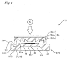
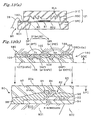
- FIG. 1 is a section showing an infrared sensing element in accordance with an embodiment of the present invention.
- An infrared sensing element 21 of this embodiment comprises a thermopile chip SPC comprising a thermopile 85 and an infrared absorber 81 which are formed on the upper surface 80a of a base 80, and a binary lens BL functioning as an infrared lens, the binary lens BL being integrated with the thermopile chip SPC by junction so that it can be handled as one chip. Therefore, the infrared sensing element 21 of this embodiment is referred to as the "infrared sensing chip" in some cases.
- a bonding wire 26 is connected to the thermopile chip SPC to take out output of diodes D1 and D2 formed on the thermopile 85 and the base 80 so that the temperature of a heat source such as the tympanic membrane can be measured.
- the binary lens BL functions as a lens for condensing infrared radiation on the infrared absorber 81 comprising a black body in the thermopile chip SPC. Therefore, the binary lens BL comprises a binary element BLb having a multi-step structure formed by etching one side of a semiconductor substrate BLa of silicon (Si) or germanium (Ge). The binary lens BL is joined to the base 80 so that the surface having the binary element BLb formed thereon faces the surface 80a or main surface of the thermopile chip SPC, which has the infrared absorber 81 formed thereon.
- the binary lens BL can also function as an infrared filter for cutting off visible light and transmitting infrared light from the viewpoint of the composition.
- an infrared coating BLc comprising a multilayer film of zinc sulfide (ZnS) and germanium (Ge) can be provided on the surface opposite to the binary element BLb.
- the binary lens BL can efficiently condense infrared radiation on the thermopile chip SPC.
- Fig. 1 shows the multi-step structure of the binary element BLb, which is exaggerated for the sake of ease of understanding.
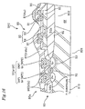
- the thermopile chip SPC of this embodiment comprises a hollow portion KW formed by removing the central portion of the bottom of a silicon substrate 810 which forms the base 80, a thin film portion 802 comprising only a thin film remaining at the top of the hollow portion KW, and a thick plate or thick wall portion 801 in which the silicon substrate 810 remains unetched to form a state referred to as a "membrane structure".
- the thin film portion 802 has a structure supported by the hollowed silicon substrate 810.
- the infrared absorber 81 is formed on the upper surface of the thin film portion 802 by depositing gold black by a sputtering, evaporation process or the like.
- the thick wall portion 801 in which the silicon substrate 810 remains comprises the two diodes D1 and D2 for detecting the reference temperature of the thermopile 85.
- Fig. 2 is a perspective view showing the thermopile chip SPC
- Fig. 3 is an enlarged view of the construction on the main surface 80a of the thermopile SPC.
- the infrared absorber 81 having substantially a square and flat shape is provided on the thin film portion 801 at the center of the main surface 80a of the thermopile chip SPC, and the hot junctions 83 of highly-sensitive thermocouples 82 are arranged near the infrared absorber 81 or to be overlapped with the infrared absorber 81.
- the cold junctions 84 of the thermocouples 82 are provided on the thick wall portion 801 in which the silicon substrate 810 remains.
- each of the thermocouples 82 produces electromotive force between the hot junction 83 and the cold junction 84 according to the temperature rise of the infrared absorber 81.
- each of the thermocouples 82 does not produce sufficient electromotive force, and thus a plurality of the thermocouples are connected in series to form the thermopile 85.
- the terminals 86 and 87 provided on the main surface 80a serve as output terminals of the thermopile 85, and the potential difference between the hot and cold junctions of the thermopile 85 can be obtained as a voltage between both terminals.
- thermopile chip SPC of this embodiment can be considered as being divided into a hot junction supporting region 66 for supporting the hot junctions 83 and the infrared absorber 81, a cold junction supporting region 67 for supporting the cold junctions 84, and an intermediate supporting region 68 for connecting the regions 66 and 67 and supporting conductors 91 and 92.
- the thin plate or thin film portion 802 constitutes the hot junction supporting region 66 and the intermediate supporting region 68
- the thick plate or thick wall portion 801 constitutes the cold junction supporting region 801.
- the hollow portion KW is formed at the back of the base 80.
- the hollow portion KW decreases heat conduction as compared with a case in which a heat conducting medium is present.
- the hollow portion KW can also be said to have a heat insulating function. Therefore, the hollow portion KW can decrease the amount of heat conduction from the infrared absorber 81 and the hot junctions 83, which are located in the hot junction supporting region 66, to the cold junctions 84, to maintain the temperature difference between the hot junctions 83 and the cold junctions 84. Therefore, the electromotive force of each of the thermocouples 82, which constitute the thermopile 85, can be increased to improve the sensitivity of temperature measurement.
- the hollow portion KW can be formed by forming an oxide film (SiO), nitride film (SiN), and the like having low heat conductivity on the silicon substrate 810 having high heat conductivity, and then removing a portion of the silicon substrate 810 ranging from the back to the thin film portion 802 by an etching step of a general semiconductor manufacturing process.
- SiO oxide film
- SiN nitride film
- thermopile chip SPC of this embodiment can easily be formed by the semiconductor manufacturing process.
- the thin film portion 802 which constitutes the hot junction supporting region 66 and the intermediate supporting region 68 comprises a structural layer with low heat conductivity, such as an oxide film and nitride film
- the amount of heat conduction of the thin film portion 802 can also be decreased.
- the thick wall portion 801 which constitutes the cold junction supporting region 67 mainly comprises the silicon substrate 810, and thus the remainder of the silicon substrate 810 functions as the heat sink because silicon has high heat conductivity.
- the temperature of the hot junction supporting region 66 is increased by infrared radiation, while the cold junctions 84 are maintained at the environment temperature, thereby securing the large temperature difference between the hot junctions 83 and the cold junctions 84 to increase the electromotive force of each thermocouple 82.
- thermopile chip SPC of this embodiment even when the infrared absorber 81 receives infrared radiation from the heat source at a temperature of as high as about 500°C relative to the reference temperature, the short-term temperature rise of the infrared absorber 81 is as small as about 1°C or less. Therefore, in view of measurement of below-freezing temperature to 1000°C or more, the temperature of the thermopile chip SPC itself less changes, and thus deformation or deterioration less accompanies this temperature change. Therefore, the thermopile chip SPC has the advantage that it less deteriorates as an infrared sensor, and stable measurement can be made over a long period of time.
- thermopile chip SPC is preferably provided, in which sensitivity is improved as much as possible to permit measurement within a short time.
- thermocouples 82 are connected in series to form the thermopile 85 in order to improve sensitivity, thereby securing large electromotive force.
- Each of the thermocouples 82 comprises two types of conductors including a first conductor of polysilicon (Si-P) 92 and a second conductor of aluminum (Al) 91.
- the polysilicon conductors 92 are formed in a line pattern to extend from each side of the infrared absorber 81.
- thermocouples 82 are connected in series to form the thermopile 85.
- thermopile infrared sensor In order to improve sensitivity, it is important to increase the temperature of the hot junction portion of the thermopile as much as possible, and bring the cold junction portion as near to the measurement environmental temperature as possible, thereby securing the temperature difference between both junctions. This is because electromotive force of each of the thermocouples, i.e., the potential difference between both junctions of each thermocouple, can be increased.
- the length of each thermocouple is preferably decreased for decreasing the size of the thermopile chip SPC, and thus the distance between the cold junction and the hot junction is decreased to make it difficult to secure the temperature difference.
- thermopile chip SPC of this embodiment in order to increase the sensitivity of temperature measurement while decreasing the size of the thermopile chip SPC, slits 98 are provided in the intermediate supporting region 68 for supporting the conductors 91 and 92, which constitute the thermocouples 82, i.e., between a pair of the conductors 91 and 92 of each thermocouple 82 and the conductors 91 and 92 of the adjacent thermocouples 82 in the thin film portion 802, so that the slits 98 communicate with the hollow portion KW on the back side from the main surface 80a.
- the slits are formed to extend in parallel to the conductors 92.
- thermocouples 82 which is a partial sectional view of Fig. 4, openings are provided between the electrodes of the thermocouples 82 to decrease the cross section of the thin film portion 802 between the hot junctions 83 and the cold junctions 84. Therefore, the cross section of the heat flow passage between the hot junction 83 and the cold junction 84 of each thermocouple is decreased to decrease the amount of heat conduction. As a result, even when the distance between the hot junction 83 and the cold junction 84 of each thermocouple is decreased, the amount of heat conduction from the infrared absorber 81 can be suppressed to suppress a change in temperature on the cold junction side. Therefore, the electromotive force of each thermocouple 82 can be increased to increase the measurement sensitivity, and thus the thermopile chip SPC of this embodiment has the construction suitable for forming the compact infrared sensing element 21 with high sensitivity.
- the cross section can be decreased by decreasing the thickness of the thin film portion 802, it is possibly difficult to control the thickness.
- the holes or slits 98 which pass through the thin film portion 802 can be formed at the same time as the hollow portion KW in the etching step of forming the hollow portion KW or in a series of subsequent steps, exhibiting excellent productivity.
- the cross section of the thin film portion 802 can be decreased without increasing the interval between the conductors 92 of the thermocouples 82, each of which connects the hot junction 83 and the cold junction 84.
- thermocouples 82 can be formed closely in the direction perpendicular to the length direction of the electrodes 92, and many thermocouples 82 can thus be formed in the compact thermopile chip SPC to form the thermopile 85 exhibiting high output voltage and high sensitivity.
- the thermopile chip SPC further comprises two conductor layers DN and DP which are formed on the main surface 80a of the semiconductor substrate 810 to surround the cold junctions 84 in the peripheral thick wall portion 801.
- the conductor layer DN comprises a N+ region with a high dose of donor impurity, and is located on the outer peripheral side and divided into two regions DN1 and DN2 which are formed in a L-shape and symmetric with respect to a point along the periphery of the base 80.
- the conductor layer DP comprises a P+ region with a high dose of acceptor impurity, and is formed inside of the regions DN1 and DN2 opposite to the regions DN1 and DN2.
- the conductor layer DP has a continuous shape
- the conductor layer DP is divided into two regions denoted by DP1 and DP2 opposite to the regions DN1 and DN2, respectively, in Fig. 2. Therefore, the regions DN1 and DP1 and the regions DP12 and DP2 form two PN junctions on the semiconductor substrate 810. Assuming that the regions DP1 and DP2 form an anode region, and the regions DN1 and DN2 form a cathode region, two diodes D1 and D2 are formed by the regions DN1 and DP1, and the regions DN2 and DP2.
- each of the PN junctions is referred to as a "diode".
- the two diodes D1 and D2 are formed in a strip shape along every side of the thick wall portion 801 so as to surround all sides of the infrared absorber 81.
- the diodes D1 and D2 are also formed to surround the cold junctions 84 of the thermopile 85 in the vicinity of the cold junctions 84.
- the temperatures of the diodes D1 and D2 can be determined by outputs from the diodes D1 and D2. Therefore, the diodes D1 and D2 are formed in the thick wall portion 801 serving as the heat sink so that the diodes can be used as the thermosensitive portions of reference temperature sensing means 70 for determining the reference temperature Tr as the temperature of the cold junctions 84 of the thermopile 85.
- an anode terminal DA common to the diodes D1 and D2, and cathode terminals DK1 and DK2 of the diodes D1 and D2 are provided on the main surface 80a, for supplying the outputs of the diodes D1 and D2 serving as the thermosensitive portions of the reference temperature sensing means 70 to the outside.
- thermopile chip SPC which constitutes the infrared sensing element 21 of this embodiment
- the diodes D1 and D2 serving as the thermosensitive portions are formed directly in the thick wall portion 801 of the base 80, which serves as the heat sink. Therefore, the temperature of the cold junctions 84 can be measured by the base 80 including the cold junctions 84.
- the cold junctions 84 and the diodes D1 and D2 are physically connected through the semiconductor substrate 810 with high heat conductivity and the semiconductor material laminated thereon, whereby the temperature of the cold junctions 84 can be measured with high accuracy.
- the distance between the diodes D1 and D2 and the cold junctions 84 is very short on the unit of mm or less. Therefore, from this viewpoint, the temperature of the cold junctions 84 can be accurately measured by the diodes D1 and D2 serving as the thermosensitive portions.
- VF ( KT / q ) log ( IF / IS )
- the equation (2) indicates that temperature T, i.e., the reference temperature Tr of the thermosensitive portion, can be measured based on the voltage drop VF of the diode D1 or D2.
- the forward current IF and the reverse saturation current IS must be determined. Since these values cannot be easily directly determined, the most practical method comprises measuring the relation between temperature and voltage, tabulating and storing the relation, and determining the reference temperature Tr based on the detected forward voltage VF.
- the temperature of the thick wall portion 801 of the base 80 can be accurately determined according to the above equation.
- Fig. 6 shows an example of an amplifier which detects the forward voltage drops VF1 and VF2 of the two diodes D1 and D2 and outputs the difference ⁇ VF.
- the amplifier 71 shown in Fig. 6 can be provided in place of, for example, the amplifier 45 of the temperature deriving circuit 400 described above with reference to Fig. 26.
- the amplifier can take outputs from the diodes D1 and D2 serving as the thermosensitive portions in contact with the base 80 to output the difference ⁇ VF which gives the reference temperature Tr with high accuracy. Therefore, the signal of the difference is digitized and processed as data of the reference temperature Tr in the CPU 44, whereby the temperature T of the heat source can be determined with high accuracy on the basis of the output from the thermopile 85.
- the amplifier 71 of this example comprises a constant current source composing a transistor J1 and resistance R1 (for example, 50 k ⁇ ), for supplying the forward current IF1 to the diode D1, and a constant current source composing a transistor J2 and resistance R2 (for example, 100 k ⁇ ), for supplying the forward current IF2 to the diode D2.
- the amplifier 71 further comprises operational amplifiers U6 and U7 for amplifying the forward voltage (the potential difference between the anode terminal DA and the cathode terminal DK1) VF1 proportional to the internal resistance of the diode D1, and the forward voltage (the potential difference between the anode terminal DA and the cathode terminal DK2) VF2 proportional to the internal resistance of the diode D2, respectively, and a differential amplifier U8 for outputting a voltage proportional to the difference between the amplified voltages VF1 and VF2. Therefore, as the output Vout of the amplifier 71, the difference ⁇ VF between the forward voltages VF1 and VF2 can be output.
- the influence of the reverse saturation current can be canceled, and the temperature can be accurately measured even when the diode characteristic of the reverse saturation current of the formed diode indicates a value different from the theoretical value.
- the resistances R1 and R2 which determine the forward currents IF1 and IF2 flowing through the two diodes D1 and D2 are different values from each other, for example, of 50 k ⁇ and 100 k ⁇
- the forward currents IF1 and IF2 can be set to different values. With the constant ratio of these values, the influence of variations in the forward currents on temperature measurement can also be removed. Therefore, even with a simple mechanism, it is possible to remove measurement error due to a difference in diode characteristics due to variations in the reverse saturation current with chips, noise, a variation in potential, and other factors of variations in measurement environment, and simply measure the temperature with high accuracy.
- each of the above equations indicates that when the diode, i.e., the PN junction, is used as the thermosensitive portion, unlike the thermistor, the output characteristic is theoretically independent of the temperature.
- the diode is suitable for the thermosensitive portion for determining the reference temperature Tr of the thermopile 85. Therefore, by utilizing the infrared sensing element 21 of this embodiment, a clinical thermometer can be provided, which has no need to limit room temperature of measurement, or which can easily measure the body temperature at any time in any place beyond the limited range of 15°C or more.
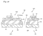
- Fig. 7 is a partial sectional view of the construction of the thermopile chip SPC of this embodiment.
- the infrared absorber 81 is formed on the thin film layer 802 having a thickness of several microns and comprising oxide films (SiO 2 ) 94 and 96 and a nitride film (Si 3 N 4 ) 97 with low thermal conductivity, in order to prevent escape of the absorbed heat to the circumference to increase a temperature rise.
- the diodes D1 and D2 are formed on the surface of the semiconductor substrate 810 directly below the cold junctions 84 serving as the principal reference point in measuring the temperature by the thermopile 85.
- the PN junction region as each of the diodes D1 and D2 is the portion 93 denoted by dotted lines in the N+ region DN1 or ND2 shown in Fig. 7.
- a thin film layer of an oxide film 94 is first formed on the surface (main surface) of the silicon substrate 810, for example, by a CVD (Chemical Vapor Deposition) method.
- a field oxide film 95 is first formed on the P-semiconductor substrate, for element separation. Then, the field oxide film is patterned, and doped with impurities to form the P+ regions DP1 and DP2 and the N+ regions DN1 and DN2. As a result, the diodes D1 and D2 are formed on the semiconductor substrate 810.
- the oxide film 94, a polysilicon layer 92 which constitutes each of the thermocouples 82, an oxide film 96 for electrode separation, an aluminum electrode 91 which constitutes each of the thermocouples 82 are formed in turn by photolithography.
- a surface protecting film 97 of silicon nitride is formed to cover these films, and gold black as a black body is deposited to form the infrared absorber 81.
- the oxide film (SiO 2 ) 94 or the like functions as a stopper to etching the back surface in forming the membrane structure, and thus the portion of the thin film layer corresponding to each of the slits 98 is removed by patterning so that the slits 98 can be simultaneously formed in the etching step of forming the membrane structure.
- thermopile infrared sensing element in principle, the electromotive force produced between the hot junctions on the infrared absorber side, which receives infrared radiation, and the cold junctions on the reference temperature side according to a change in temperature of the infrared absorber is detected to determine the temperature difference between the hot junctions and the cold junctions based on the electromotive force.
- the reference temperature is measured by another temperature sensing means. Therefore, a temperature difference between the reference temperature and the cold junction temperature causes error, deteriorating the measurement accuracy.
- the thermistor 211 for detecting the reference temperature is provided on the package substrate 212.
- the measurement accuracy is improved, as compared with a case in which the thermistor is provided outside the package, i.e., outside the chip.
- the distance between the measurement point of the reference temperature measured by the thermistor 211 and the cold junctions of the infrared sensor 209 is large, and thus the temperature of the cold junctions to be measured cannot be accurately measured as the reference temperature.
- the diodes D1 and D2 serving as the thermosensitive portions for detecting the reference temperature for the cold junctions 84 of the thermopile 85 are integrally formed on the silicon substrate 810 as the substrate of the base 80 on which the thermopile 85 is formed so that the reference temperature is detected based on the temperature characteristics of the diodes.
- the diodes D1 and D2 serving as the thermosensitive portions are arranged in contact with the base 80 and built in the base 80.
- the temperature of the heat sink of the cold junctions can be measured directly by determining the reference temperature with the thermistor in contact with the base 80, the measurement accuracy is greatly improved as compared with the conventional infrared sensing chip 210 shown in Fig. 23.
- the thermistor cannot be easily integrally manufactured in contact with the base 80.
- the diode as the thermosensitive portion, the diode can be formed integrally with the silicon substrate 810 of the base 80. Therefore, the diode and the thermopile 85 can be formed integrally with the thermopile chip SPC to significantly decrease the distance between the thermopile 85 and the diode, thereby further decreasing the measurement error of the reference temperature of the thermopile 85.
- the temperature of the cold junctions 84 to be measured can be measured as the accurate reference temperature, providing an infrared sensing element with high measurement accuracy.
- the components including the diodes D1 and D2 serving as the thermosensitive portions, the infrared absorber 81, a thermopile 85, etc. of the infrared sensing element 21 can be formed on the semiconductor substrate 810 as the substrate of the base 80 by a general method for manufacturing a semiconductor, such as CVD, or the like. Therefore, in the infrared sensing element 21 of this embodiment, the components can easily accurately be formed on the semiconductor substrate 810, and are suitable for mass production. Furthermore, the reference temperature Tr can accurately be measured, thereby providing a small infrared sensing element with high measurement accuracy at low cost.
- the thermistor Since the temperature characteristic of the thermistor greatly changes, the thermistor has the limited temperature range of about 15°C or more in which the temperature can accurately be measured. On the other hand, the characteristics of the diode have substantially no dependency on temperature, thereby permitting temperature measurement with high accuracy within the temperature range of 5°C to 40°C.
- the infrared sensing element 21 of this embodiment can thus simply be used under various environments. Furthermore, the infrared sensing element 21 of this embodiment uses the two diodes D1 and D2 for removing the influences of the reverse saturation currents and the forward currents on temperature measurement. Therefore, an infrared sensing element with higher measurement accuracy can be provided.
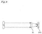
- the binary lens BL is joined to the thermopile chip SPC.
- the binary lens BL can be arranged away from the thermopile chip SPC so that the wave guide 206 is replaced by the lens.
- the binary lens BL is separated from the thermopile chip SPC. Therefore, a temperature difference possibly occurs between the binary lens BL and the thermopile chip SPC. With a temperature difference between the binary lens BL and the thermopile chip SPC, the influence of infrared radiation received through the lens BL under a different temperature environment is measured to easily cause error, possibly influencing the measurement accuracy.
- the binary lens BL is joined to the surface of the thermopile chip SPC. Therefore, the temperature difference between the thermopile chip SPC and the binary lens BL less occurs, and the above-descried error due to the binary lens BL less occurs. Furthermore, the binary lens BL is joined to the thick wall portion 801 of the base 80, and the diodes D1 and D2 serving as the thermosensitive portions are arranged near the junction between the binary lens BL and the thermopile chip SPC, for detecting the reference temperature. It is thus possible to decrease not only the measurement error due to the temperature difference between the reference temperature and the cold junction temperature, but also the measurement error due to the temperature difference between the measurement point of the reference temperature and the lens temperature.
- thermopile chip SPC thermopile chip
- an infrared sensing chip without the binary lens BL i.e., a simple thermopile chip
- Such an infrared sensing chip can be used, for example, by integrating with the clinical thermometer 100 using the wave guide 206.
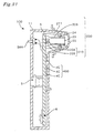
- Fig. 9 is a sectional view schematically showing an ear-type clinical thermometer 1 into which the infrared sensing element 21 of this embodiment is integrated.
- the ear-type clinical thermometer 1 comprises a body case 11, an infrared receiving sensing unit 2 which receives infrared radiation emitted from a heat source S to output an electrical signal according to the temperature of the heat source S, and a circuit board 3 on which various electronic elements (circuits) are mounted and connected.
- the various electronic parts 4C mounted on the circuit board 3 constitute a temperature deriving circuit 4 for determining the temperature of the heat source S based on the output voltage of the infrared receiving sensing unit 2.
- a LCD unit 5 for displaying the measured temperature, and the like, and an electric power source 6 for supplying electric power to each of the units are connected to the circuit board 3.
- the electric power source 6 comprises a power switch SW6, a button battery 61, and a battery terminal fitting 62 for connecting the button battery 61 mounted thereto to a circuit pattern of the circuit board 3, a portion of the case 11 constituting a battery box cover 63 which is opened and closed for changing the battery.
- the LCD unit 5 comprises a LCD panel 51 for various displays, a connector 52 for connecting the LCD panel 51 mounted thereto to the circuit board 3, and a panel frame 53 for supporting the LCD panel 51.
- a portion of the case 11 constitutes, for example, a plastic transparent cover 54 for visibly protecting the surface of the LCD panel 5.
- the infrared receiving sensing unit 2 comprises the infrared sensing element 21 of this embodiment, which constitutes the heart of the infrared receiving sensing unit 2 to receive infrared radiation corresponding to the temperature of the heat source (body temperature: temperature of the tympanic membrane) and outputting an voltage signal according to the infrared radiation, a plastic cover 22 for protecting the element 21, an infrared transmitting film 23 for preventing entrance of dust particles into the cover 22, a film holding O-ring 24 for supporting the film 23, and an infrared transmitting probe cap 25 mounted to cover the entire infrared receiving sensing unit because the infrared receiving sensing unit is inserted into the lughole during measurement of body temperature.
- the portion 211 of the case 11 which contains the infrared receiving sensing unit 2 has a cylindrical shape having a tapered front end, and the infrared sensing element 21 is provided in the portion 211 so that the binary lens BL faces the front end. Therefore, infrared radiation transmitted through the probe cap 25 mounted at the front end of the cylindrical portion 211 is condensed on the infrared absorber 81 of the thermopile chip SPC.
- the infrared sensing element 21 is also mounted on the circuit board 3, and the thermopile chip SPC is connected to the circuit board 3 with a bonding wire 26 so that outputs of the diodes D1 and D2 and output of the thermopile 85 are input to the temperature deriving circuit 4 of the circuit board 3.
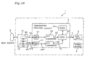
- Fig. 10 shows the temperature deriving circuit 4 of this embodiment.
- the temperature deriving circuit 4 has substantially the same configuration as the temperature deriving circuit 400 described above with reference to Fig. 26 except that the amplifier 71 shown in Fig. 6 is used for processing the forward voltage drops VF1 and VF2 of the diodes D1 and D2 which are input to the temperature deriving circuit 4.
- the difference ⁇ VF between the forward voltage drops VF1 and VF2 is converted into a digital signal by the A/D converter 46 and supplied as a signal indicating the reference temperature Tr to the CPU 44.
- the temperature measuring circuit 4 of this embodiment comprises an amplifier 41 for amplifying a signal indicating the body temperature output from the infrared sensing element 21 provided in the infrared receiving sensing unit 2, i.e., a voltage signal output from the thermopile 85, an A/D converter 42 for digitizing the output, a CPU 44 for performing numerical processing of the output value to determine the body temperature and display the temperature on the LCD 5, and a RAM 43 serving as a work area for each processing in the CPU 44.
- the temperature measuring circuit 4 further comprises the amplifier 71 for amplifying the outputs of the diode D1 and D2 of the reference temperature sensing means 70 of the sensing element 21 to output the difference ⁇ VF between both outputs, and an A/D converter 46 for digitizing the output.
- the CPU 44 performs processing for determining the temperature T from the output Vt of the thermopile 85 based on the difference ⁇ VF considered as the reference temperature Tr.
- the power source switch SW6 and the temperature measurement switch SW4 shown in Fig. 9 are connected to an input port of the CPU 44 so that when the power source is turned off in the initial state, the CPU 44 is in a stand-by state, while the other circuits are in a non-conduction state.
- the CPU 44 detects a level change as an interrupt signal and is brought into an active state, while the other circuits are brought into a conduction state.
- the CPU 44 When the CPU 44 is activated, the CPU 44 first displays "all lighting" (initial display) on the LCD panel 51, and then makes preparation for measurement, such as initialization of various flag or the like. After the preparations are completed, the CPU 44 displays that "preparation for measurement is OK".
- the CPU 44 activates the A/D converters 42 and 46 to obtain the output Vt from the infrared sensing element 21 as a digital value through the amplifier 41 and the A/D converter 42.
- the CPU 44 also obtains the outputs VF1 and VF2 from the diodes D1 and D2 as digital values through the amplifier 71 and the A/D converter 46.
- the CPU 44 determines the reference temperature from the output from the A/D converter 46 while correcting the output with the offset voltage of each amplifier, and computes the temperature T from the output from the A/D converter 42 based on the reference temperature.
- the value T is displayed as a measurement result on the LCD panel 51 accompanied with beeping for information, and the A/D converters 42 and 46 are inactivated.
- the power source switch SW6 is pushed, or when the power source switch SW6 and the temperature measurement switch SW4 are not operated within a predetermined time thereafter, the power source is turned off in the initial state by auto-power off.
- the user In use of the ear-type clinical thermometer 1, the user first pushes the power source switch SW6 and recognizes that the LCD panel 53 is changed from the initial display to the display of "OK measurement preparation”. Then, the probe cap 25 is inserted into the lughole, and the temperature measurement switch SW4 is pushed to start measurement. Several seconds after, the measurement value is displayed on the LCD panel 51 accompanied with an information sound, and thus the value (body temperature) can be recognized. Then, the power source switch SW6 is pushed, or the thermometer 1 is allowed to stand to turn the power source off by auto-power off.
- the small low-cost infrared sensing element 21 of this embodiment which is capable of measuring temperature with high accuracy, is incorporated into the infrared sensing unit 2, and thus the ear-type clinical thermometer itself is a small low-cost device capable of measuring temperature with high accuracy.
- the ear-type clinical thermometer 1 does not use the wave guide.
- the angle of view from the window plane (sensing plane) of the infrared filter 23 is about 180°, and thus infrared radiation from the outside of the wave guide 206 is also incident.
- infrared radiation in the wave guide 206 is subjected to interference due to external heat Sd. Furthermore, light diffusely reflected due to the interference in the wave guide is incident on the sensing plane to increase measurement error.
- the ear-type clinical thermometer 1 of this embodiment comprising the infrared sensing element 21 using the binary lens BL for concentrating infrared radiation on the thermopile chip SPC, whereby the angle of incidence of infrared radiation can be restricted. Therefore, it is possible to decrease the error due to incidence of infrared radiation, and measure the body temperature with high accuracy as compared with the clinical thermometer using the wave guide 206. Since the infrared sensing chip 21 in which the binary lens BL and the thermopile chip SPC are integrally connected together is used, substantially no error occurs in measurement due to the difference between the reference temperature and the lens temperature.
- the ear-type clinical thermometer 1 can measure the temperature of the human tympanic membrane as the heat source and display the temperature as the body temperature T.
- the present invention is not limited to the above embodiment, and includes various modifications.
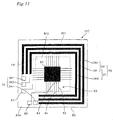
- arrangement of the P+ region DP and the N+ region DN can be freely changed.
- the two diodes D1 and D2 are arranged along the periphery of the main surface 80a so as to be opposed to each other with the infrared absorber 81 formed therebetween, the diodes D1 and D2 may be formed in parallel along the periphery of the main surface 80a, as shown in a plan view of Fig. 11 and a sectional view of Fig. 12.
- a common conductor layer may be used as the conductor layers of one side, which constitute the two diodes D1 and D2.
- the N+ region DN1 and N+ region DN2 are formed with the P+ region DP provided therebetween so that the three conductor regions form the two diodes D1 and D2.
- the diodes D1 and D2 are arranged in parallel along the periphery of the main surface 80a so that the diodes D1 and D2 can be arranged along a plurality of cold junctions 84 of the thermopile 85. Therefore, an average temperature of the cold junctions 84 can be determined as the reference temperature Tr. Furthermore, the arrangement of the diodes D1 and D2 is not limited to this, and an appropriate arrangement can be selected in view of temperature characteristics and the yield of manufacture of the thermopile chip. As the arrangement of the electrodes DK and DA, a different arrangement can be used in view of ease of handling of wiring and distribution of terminals, etc.
- the number of the diodes formed on the thermopile chip SPC is not limited to two, and the number may be one as described above. The number may also be three. However, at least two diodes are preferably arranged to determine the difference between forward voltage drops, whereby the reference temperature Tr can be measured with high accuracy. In addition, the reference temperature may be determined based on the average of the forward voltages VF of the plurality of diodes so that data processing is performed to cancel a difference in the formation positions or the diodes, a difference in characteristics or environments, and a deviation from the theoretical value or design value.
- the diodes D1 and D2 are formed on the semiconductor substrate 810 directly below the cold junctions 84, thereby greatly decreasing measurement error based on the distance from the cold junctions and an environmental difference.
- the diodes D1 and D2 may be formed not only on the silicon substrate 810 but also on the junction of the binary lens BL joined to the base 80 or the another semiconductor substrate superposed on the silicon substrate 810. Namely, in the infrared sensing element 21, the binary lens BL is joined to the surface of the thermopile chip SPC to form the infrared sensing chip as a unit.
- the diodes D1 and D2 may be provided on another member such as the binary lens BL or the like and joined to the base 80 as long as the diode position satisfies the conditions that it is near the junction between the binary lens BL and the thermopile chip SPC and near the cold junctions as the principal reference point.
- the reference temperature can be measured with the thermosensitive portion in contact with the base 80.
- Fig. 13(a) shows an example of the infrared sensing element 21 in which the diodes D1 and D2 are formed on the binary lens BL side, not on the thermopile chip SPC.
- the diodes D1 and D2 can be arranged in contact with the base 80 on which the thermopile 85 is formed, as long as the diodes are provided on a member joined to the thermopile chip SPC, such as the binary lens BL.
- the diodes are connected to the thick wall portion 801 serving as the heat sink through a thermal conducting material such as a silicon-based or germanium-based semiconductor material or metal material, not in an indirect state where air is present between the diodes and the base 80.
- a thermal conducting material such as a silicon-based or germanium-based semiconductor material or metal material
- the binary lens BL is divided into a diode chip DDC and a binary lens chip BLC which are laminated in this order on the thick wall portion 801 of the thermopile chip SPC.
- the diodes D1 and D2 are formed on the diode chip DDC at the junction 190 with the thermopile chip SPC.
- the diodes may be formed on the binary lens BL at the junction with the thermopile chip SPC, and the junction may be joined to the thick wall portion of the base 80 for detecting the reference temperature.
- the binary lens is preferably divided into the lens chip BLC and the diode chip DDC to separate the manufacturing steps, thereby simplifying combination of the processes and easily improving yield.
- the measure of adding zinc sulfide (ZnS) and germanium (Ge) to the composition of the lens chip BLC can impart the function as an infrared filter for cutting off visible light to the binary lens.
- the wavelength region can be narrowed by an infrared coating comprising a multilayer film of zinc sulfide and germanium.
- a binary element BLb having a multi-step structure may be formed to facilitate formation of lenses with the same light collecting accuracy, as compared with general lenses each comprising a curved surface.
- all the binary lens chip BLC, the diode chip DDC and the thermopile chip SPC, which constitute the infrared sensing element, can be formed by a semiconductor manufacturing process such as etching or the like using a silicon or germanium semiconductor substrate.
- a semiconductor manufacturing process such as etching or the like using a silicon or germanium semiconductor substrate.
- an oxide film 105 is first formed on the surface (the lower surface shown in the drawing) of the silicon substrate 180 of the diode chip DDC.
- the oxide film 105 is patterned and doped with ions to form the P+ regions DP1 and DP2 and the N+ regions DN1 and DN2 which constitute the diodes D1 and D2, respectively.
- an oxide film 106 is formed, and aluminum metal layers of diode anode patterns DAP1 and DAP2, and diode cathode patterns DKP1 and DKP2 are formed. Furthermore, a thin film layer comprising a nitride film 107 for protecting those films is formed, and at the same time, anode terminals DAT are formed.
- the P+ regions DP1 and DP2 and the N+ regions DN1 and DN2 are preferably arranged so that at the junction 190 of the diode chip DDC, the PN junction region 103 is located directly below the cold junctions 84 of the thermopile 85 when the diode chip DDC is joined to the thermopile chip SPC. Therefore, in joining the diode chip DDC and the thermopile chip SPC together, the diodes D1 and D2 serving as the thermosensitive portions are arranged in contact with the cold junctions 84 serving as the principal reference point for sensing the reference temperature, whereby the reference temperature of the cold junctions 84 directly below the diodes or the vicinity thereof can be measured with high accuracy.
- the diode chip DDC comprises a junction substrate having a central opening formed to apply infrared radiation to the central infrared absorber 81 of the thermopile chip SPC so that the junction 190 with the thermopile chip SPC has a ring shape.
- the two diodes D1 and D2 are formed to extend along the ring junction 190.
- the diode cathode pattern DKP1 connected to the cathode terminal DKT1, the corresponding N+ region DN1, the diode cathode pattern DKP2 connected to the cathode terminal DKT2, and the corresponding N+ region DN2 are formed in substantially a ring shape.
- the diode anode pattern DAP1 connected to the common anode terminal DAT and extending in one of the two directions, the corresponding P+ region DP1, the diode anode pattern DAP2 connected to the above-described anode terminal DAT and extending in the other of the two directions, the corresponding P+ region DP2 are also formed in substantially a ring shape.
- terminals DA, DK1 and DK2 are also provided on thermopile chip SPC, which serve as diode output terminals of the infrared sensing element 21 when the diode chip DDC is joined to the thermopile chip SPC.
- These terminals are connected, with aluminum wiring, to terminals DAS, DKS1 and DKS2, respectively, for connecting to the diode chip DDC.
- the connecting terminals DAS, DKS1 and DKS2 are arranged opposite to the terminals DAT, DKR1 and DKT2, respectively, of the diode chip DDC. Therefore, as shown in Figs.
- the connecting terminals DAS, DKS1 and DKS2 can be connected to the terminals DAT, DKT1 and DKT2, respectively, by inserting a soft metal of solder 110 between the aluminum layers which constitute opposite terminals.
- the output terminals DA, DK1 and DK2 are arranged in the region of the surface 80a of the base, which extends outside the junction region with the diode chip DDC, whereby the infrared sensing element 21 exhibiting ease of bonding can be provided.
- the diodes D1 and D2 are formed on the binary lens BL or the junction of another substrate joined directly to the thermopile chip SPC, thereby permitting arrangement of the diodes D1 and D2 in contact with the thick wall portion 801 serving as the heat sink of the thermopile chip SPC. Therefore, the temperature of the cold junctions 84 of the thermopile chip 85 can be detected as the reference temperature by using the diodes D1 and D2 as the thermosensitive portions, permitting temperature measurement with high accuracy.
- the diodes are arranged on a chip different from the thermopile chip SPC to save the space for arranging the diodes on the thermopile chip SPC, and thus the smaller infrared sensing element as a whole can be provided.
- the binary lens BL, the diode chip DDC and the thermopile chip SPC can be produced by using the semiconductor manufacturing process. Therefore, the configuration is suitable for mass production, and a compact infrared sensing element with high sensitivity can be provided at low cost.
- the binary lens BL is joined to the thermopile chip SPC, or a combination of the binary lens chip BLC and the diode chip DDC is joined to the thermopile chip SPC, as in this embodiment, so that the temperature of the binary lens BL agrees with the temperature of the thick wall portion 801 serving as the heat sink to decrease the influence or interference of infrared radiation due to external heat. It is thus possible to decrease the factors of error to further improve the measurement accuracy.
- the junction between the binary lens serving as infrared lens and the thermopile chip can be used as the space for the thermosensitive portions, thereby making the element compact.
- the temperature (equal to the reference temperature because of contact with the thermopile chip) on the binary lens BL side is also determined by the diodes D1 and D2, thereby decreasing the measurement error, decreasing the measurement error due to the temperature difference between the reference temperature and the lens temperature.
- the substrate referred to as "the diode chip" for forming the diodes D1 and D2 is a junction substrate composed of semiconductor, and formed by processing for joining binary lens chip (lens substrate) BLC. Therefore, the shape of the diode chip is not limited to the above shape, and an appropriate shape coinciding with the shape of the lens chip and the shape of the thermopile chip can be formed so that the binary lend chip BLC having a shape suitable for the lens can be appropriately joined to the thermopile chip SPC having a shape suitable for an infrared sensor.
- the terminals are arranged together on one side of the thermopile chip SPC so that the bonding wire 26 can be led from one side
- the terminals can be formed on both sides, or the thermopile chip SPC can be formed in a size larger than the binary lens BL (the binary lens chip BLC + diode chip DDC) so that the terminals can be distributed in the periphery of the chip to take out signals from all regions.
- the diode anode patterns DAP1 and DAP2 and the diode cathode patterns DKP1 and DKP2 are provided in contact with the P+ regions DP1 and DP2 and the N+ regions DN1 and DN2, which are diode conductor regions, to remove a potential difference between positions where the potentials should be the same as a diode, thereby securing an accurate operation.
- the P+ regions DP1 and DP2 and the N+ regions DN1 and DN2 can be connected directly to the terminals DAT, DKT1 and DKR2 to omit the patterns DAP1, DAP2, DKP1 and DKP2, etc.
- the conductor region is lengthened, and thus, like in this embodiment, the patterns are preferably provided to prevent the occurrence of a potential difference.
- the diodes D1 and D2 are formed on the thermopile chip SPC.
- the diode anode patterns DAP1 and DAP2 and diode cathode patterns DKP1 and DKP2 are provided on the thermopile chip SPC to remove a potential difference between positions where the potentials should be the same as a diode, thereby securing an accurate operation.
- the diodes cannot be easily formed directly below the cold junctions 84, but the diodes D1 and D2 can be arranged sufficiently near the cold junctions 84, whereby the reference temperature can be measured with the same or higher accuracy as or than the above embodiment.
- thermocouples 82 As the material of the conductor for forming the thermocouples 82, a material having low resistivity and low thermal conductivity is preferred. Therefore, a semiconductor from which a material with low resistivity and low thermal conductivity can be obtained is frequently used, as compared with a metal which has low resistivity but is liable to increase in thermal conductivity. Namely, it is possible to use a semiconductor material having an absolute thermoelectric ability (i.e., Seebeck coefficient) of ten times as high as an ordinary metal, the thermoelectric ability representing thermoelectric force per unit temperature. Therefore, in the above embodiment, as one of the conductors which form each of the thermocouples 82, polysilicon doped with V-group element phosphorus P as a donor impurity is used.
- an absolute thermoelectric ability i.e., Seebeck coefficient
- the polysilicon is an n-type semiconductor, but it can be changed to a semiconductor material having lower resistivity and lower thermal conductivity.
- a p-type semiconductor doped with a III-group element as an acceptor impurity can be used as the conductor for the thermocouples 82.
- aluminum, (phosphorus-dope) polysilicon, molybdenum silicide, titanium nitride, tungsten silicide, or the like can be used as the other conductor of each of the thermocouples 82.
- each of the thermocouples 82 may be made of a combination of p-type semiconductor and n-type semiconductor.
- the Seebeck coefficients of the p-type semiconductor and n-type semiconductor have opposite polarities, the p-type semiconductor and n-type semiconductor can be alternately connected in series to form a thermopile.
- a metal having lower resistivity can be used only in the portions corresponding to the hot junctions and cold junctions.
- thermopile In general, in consideration of the coefficient of the thermopile, the performance coefficient, Peltier coefficient, Thomson coefficient of each material used for the thermopile, etc. based on the Kelvin relationship and the efficiency equation of Carnot cycle, etc., a high efficiency can be attained, and the sensitivity of the thermopile can be improved. Even in use of a metal for one of both conductors, the spaces between the hot junctions and cold junctions can be relayed with a metal or a semiconductor having low thermal conductivity to improve measurement sensitivity.
- the slit 98 is provided between one of the conductors of each thermocouple 82, for example, the other conductor of the thermocouple 82 adjacent to an aluminum electrodes 91, and a polysilicon electrode 92.
- the thermal conduction between the hot junctions 83 and cold junctions 84 can be decreased to secure the large temperature difference between both junctions, thereby increasing the electromotive force produced in each of the thermocouples 82. Therefore, even when the distance between the hot junctions and cold junctions is decreased to make the element compact, the infrared sensing element 21 having high sensitivity can be provided. It is thus preferable to widen the slits 98. However, since the distance between the respective conductors must be increased, it is difficult to compactly arrange many thermocouples, possibly increasing the chip area.
- an oxide film 99 may be provided on the polysilicon layer 91, which is one of the conductors of each thermocouple 82, and the aluminum layer 92, which is the other conductor, is formed on the oxide film 99 to be overlapped with the conductor 91.
- This can decrease the planar space occupied by the conductors 91 and 92, and thus permit the formation of the wide slits 98 between the conductors 91 and 92.
- the packing density of the thermocouples 82 can be further increased. Therefore, the size of the slits 98 can be further increased to improve measurement sensitivity without a change in the total surface area of the chip.
- the slit 98 may be provided within the width of one or both of the conductors which constitute each thermocouple.
- the slit 98 is provided in the polysilicon layer 92 of each thermocouple 82 so as to continue from the surface of the polysilicon layer 92 to the hollow portion KW, thereby decreasing the sectional area of the conductors. It is thus possible to decrease the amount of the heat transmitted through the conductors 92, and thus increase the sensitivity of the thermocouples. In this case, the packing density of the thermocouples 82 is not decreased.
- the holes are not limited to the slits.
- the holes do not necessarily pass through the thin film portion 802 to reach the hollow portion KW, and a recess may be formed in a portion of the thin film portion 802 or the conductor 92 or 91 which constitutes each of the thermocouples 82 to decrease the sectional area between the hot junction and cold junction, thereby decreasing the amount of heat conduction to improve sensitivity.
- thermopile chip SPC comprising the infrared absorber 81
- the thin film portion 802 formed by the hollow portion KW permits achievement of a sensor with sufficiently high sensitivity to infrared radiation.
- the silicon substrate 810 remaining unetched in the thin wall portion 801 functions as the heat sink. Therefore, even when the infrared absorber 81 is not formed on the thin film portion 802, the present invention can provide an infrared sensing element with sufficiently high sensitivity, which can be used as a clinical thermometer or the like.
- the infrared absorber 81 absorbs infrared radiation to increase temperature, and thus the temperature difference between the thin film portion 802 and the thick wall portion 801 can be increased, thereby increasing the output voltage of the thermopile 85 and further improving measurement sensitivity.
- the ear-type clinical thermometer is described as an example of the temperature measuring device using the infrared sensing element 21 of the present invention.
- the present invention can be applied to not only other types of clinical thermometers in which the temperature of a heat source is measured by using infrared radiation from the heat source, but also temperature measuring devices for other applications.
- the measured temperature can be used by various methods, and, for example, the measured temperature can be displayed or used for performing various controls. Therefore, the present invention is not limited to temperature measuring devices having only the function to measure temperatures, and the present invention includes devices having a combination with another function, for example, a control function.
- the above-described embodiment is only an example of the present invention, and an appropriate change can be made within the scope of the appended claims.
Description
- The present invention relates to a thermopile infrared sensing element and a temperature measuring device using the same.
- A known temperature measuring device uses an infrared sensing element which detects infrared radiation emitted from a heat source and converts it into an electric signal. Examples of known infrared sensing elements include a thermopile type, a pyroelectric type, a bolometer and the like. The thermopile infrared sensing element utilizes the Seebeck effect of a thermopile comprising a thermocouple or a plurality of themlocouples connected in series, for detecting a temperature change due to infrared radiation or absorption as thermoelectromotive force. The pyroelectric infrared sensing element detects a temperature by using a change in floating charge due to polarization according to the infrared thermal energy, i.e., a pyroelectric effect, of a base material comprising ceramic or the like. The borometer comprises a thermosensitive resistor comprising a thin film or a thin wire of a metal or the like so that a thermal change in resistance value of the resistor is detected.
- Of these sensing elements, the pyroelectric infrared sensing element requires a shutter provided on an optical path, for alternately measuring the temperatures of a surface to be measured and a reference point because polarization occurs only at the moment of application of thermal energy. Therefore, it is difficult to miniaturize the pyroelectric infrared sensing element and improve measurement accuracy. The pyroelectric infrared sensing element can thus be used for applications such as a "body sensing element" of an automatic door and the like, which are not usually required to have a small size or high measurement accuracy. However, the pyroelectric infrared sensing element is unsuitable for a temperature measuring device such as a clinical thermometer or the like, which is required to measure temperatures with high accuracy and have a small size and low cost.
- Furthermore, the pyroelectric and thermopile infrared sensing elements require detecting a relative temperature difference from a reference temperature, while the borometer has the advantage that an absolute temperature can be measured. However, the borometer has many causes of error, such as self heating due to measuring current, current noise, etc., thereby causing difficulties in improving the measurement accuracy. The borometer also requires a bias current to complicate the structure, thereby complicating handling.
- On the other hand, the thermopile infrared sensing element does not use such a transient phenomenon as utilized by the pyroelectric type and such excess measuring current as flowing through the borometer, and thus the thermopile infrared sensing element can stably detect or measure temperatures. Furthermore, the thermopile infrared sensing element can be miniaturized by using the semiconductor manufacturing process at low cost, and is thus suitable for a temperature measuring device such as a clinical thermometer or the like, which is required to be small in size and inexpensive.
- Fig. 21 shows an ear-type
clinical thermometer 100 as a temperature measuring device using a thermopile infrared sensor or infrared sensing element. The ear-typeclinical thermometer 100 comprises abody case 11, an infrared receivingsensing unit 200 which receives infrared radiation from the ear to output a voltage signal according to the temperature of the ear, i.e., the temperature of the tympanic membrane, and acircuit board 3 on which various electronic parts and circuits are mounted. On thecircuit board 3, variouselectronic parts 4C are mounted to form atemperature deriving circuit 400 for determining the temperature of the tympanic membrane based on the output voltage of the infraredreceiving sensing unit 200, or the body temperature based on the temperature of the tympanic membrane. Furthermore,LCD 5 for displaying the determined temperature, and the like, and apower source 6 for supplying electric power to each of the units are also mounted on thecircuit board 3. - The infrared receiving
sensing unit 200 comprises acase 211 having a cylindrical shape which projects forward (to the right of the drawing) to permit the front end to be inserted into the lughole, awave guide 206 contained in thecase 211, and aninfrared sensing chip 210 arranged at the base of thewave guide 206 to face the front end of thecase 211. The front end of thecase 211 is open, and covered with an infraredtransmitting probe cap 25, and the front opening of thewave guide 206 is covered with an infrared transmittingfilm 23 for preventing entrance of dust particles, etc, thefilm 23 being supported by a film holding O-ring 24. Therefore, when the front end of thecase 211 is inserted into the lughole, infrared radiation entering the infrared receivingsensing unit 200 is guided to theinfrared sensing chip 210 by thewave guide 206 so that theinfrared sensing chip 210 receives the infrared radiation corresponding to the temperature of the tympanic membrane to output a voltage signal according to the infrared radiation. Therefore, when a temperature measurement switch SW4 of the ear-typeclinical thermometer 100 is pushed, the body temperature can be measured by the infrared receivingsensing unit 200 through infrared radiation. - Namely, the
clinical thermometer 100 is a wave guide type in which infrared radiation entering from a heat source (the lughole) S is transmitted through thewave guide 206 arranged in front of theinfrared sensing chip 210 to be guided to theinfrared sensing chip 210, as shown in Fig. 22. The temperature rise due to the infrared radiation is converted into a voltage by the thermopile of theinfrared sensing chip 210 and then output. - Fig. 23 shows the
infrared sensing chip 210. Theinfrared sensing chip 210 comprises a thermopileinfrared sensor 209, and athermistor 211, both of which are mounted on apackage substrate 212. In theinfrared sensing chip 210, thethermistor 211 is used for determining the reference temperature of the thermopile formed in theinfrared sensor 209, i.e., the temperature of the cold junction. These components are contained in apackage case 213 to unify the components. Thepackage case 213 further comprises aninfrared filter 208 composed of silicon or the like and provided in a window which infrared radiation enters, for cutting-off visible light and transmitting infrared radiation. - Fig. 24 is a perspective view schematically showing the infrared sensor or
infrared sensing element 209. Theinfrared sensor 209 comprises abase 80 comprising a portion (thin film portion) 802 in which only a thin film is left by etching a silicon substrate to form a hollow at the center of the lower surface or the bottom of the silicon substrate, and athick wall portion 801 in which the silicon substrate remains unetched. Namely, theinfrared sensor 209 has a structure in which a hollow portion KW is formed at the center of thebase 80 from the lower side to form a membrane at the top of thebase 80.
Furthermore, gold black is deposited at the top of thethin film portion 802 by sputtering, evaporation, or the like to form aninfrared absorber 81 comprising a black body for absorbing infrared radiation. The infrared absorber 81 absorbs infrared radiation to cause a change in temperature. - The
infrared sensor 209 further comprises a plurality ofthermocouples 82 with high sensitivity, which are provided on every side of theinfrared absorber 81. Thehot junction 83 of each of thethermocouples 82 is arranged near theinfrared absorber 81 or to be overlapped with it, and thecold junction 84 of eachthermocouple 82 is arranged in the peripheralthick wall portion 801 in which the silicon substrate remains. Although electromotive force occurs between thehot junction 83 and thecold junction 84 of eachthermocouple 82 according to a temperature rise of theinfrared absorber 81, the electromotive force produced by asingle thermocouple 82 is not sufficient. Therefore, theinfrared sensor 209 comprises a plurality ofthermocouples 82 which are connected in series to form athermopile 85 so that a voltage between both ends serving as a terminal (for example, + terminal) 86 and a terminal (for example, - terminal) 87 can be output. - More specifically, as shown in Fig. 25, each of the
thermocouples 82 comprises two types of conductors of aluminum (A1) 91 and polysilicon (Si-P) 92. Thepolysilicon 92 is deposited in a line shape. The end of each of thepolysilicon conductors 92, which is arranged near theinfrared absorber 81, i.e., which is arranged in thethin film portion 802, is joined to thealuminum wiring 91 to form thehot junction 83. On the other hand, the end of eachpolysilicon conductor 92, which is arranged in thethick wall portion 801 functioning as a heat sink, is joined to thealuminum wiring 91 to form thecold junction 84. Eachaluminum wiring 91 connects thehot junction 83 and thecold junction 84 of theadjacent polysilicon conductors 92, resulting in a state where thethermocouples 82 are connected in series. - Fig. 26 is a block diagram schematically showing the functional configuration of the ear-type
clinical thermometer 100. The ear-typeclinical thermometer 100 comprises thetemperature deriving circuit 400 to which a temperature sensing voltage Vt between bothterminals thermopile 85 of theinfrared sensor 209 is input to output temperature T based on the voltage Vt to theLCD 5. Thetemperature deriving circuit 400 comprises anamplifier 41 for amplifying the temperature sensing voltage Vt, an A/D converter 42 for converting the output from theamplifier 41 to a digital value,CPU 44 for performing numerical processing of the digital value to determine the temperature corresponding to the temperature sensing voltage Vt, andRAM 43 serving as a working area for each processing in theCPU 44. Thetemperature deriving circuit 400 detects the electromotive force produced between thehot junctions 83 and thecold junctions 84 of thethermopile 85 of theinfrared sensor 209 according to a change in temperature to determine the temperature difference Ts between thehot junctions 83 and thecold junctions 84 based on the output voltage Vt. In order to determine the temperature of the infrared absorber 81 to calculate the body temperature T (herein, the temperature of the tympanic membrane), the temperature (reference temperature) of thecold junctions 84 must be determined for correction. - Therefore, the
infrared sensing chip 210 contains thethermistor 211 so as to detect the reference temperature Tr of theinfrared sensor 209. Thetemperature deriving circuit 400 further comprises anamplifier 45 for amplifying the output current It of thethermistor 211, and an A/D converter 46 for converting the output to a digital value to supply a digital signal to theCPU 44. TheCPU 44 can thus correct the temperature difference Ts obtained by the signal from thethermopile 85 with the reference temperature Tr obtained by thethermistor 211 to determine the body temperature T. - However, as shown in Fig. 23, the
thermistor 211 simply measures the temperature on the side of theinfrared sensor 209, i.e., the environmental temperature around theinfrared sensor 209 within the infrared detectingchip 210. Therefore, the temperature detected by thethermistor 211 is different from the actual temperature of thecold junctions 84, thereby possibly causing great error in the body temperature T determined as described above. - The
thermistor 211 is apparently suitable for measuring the reference temperature in view of the fact that the absolute temperature can be measured because the resistivity changes with temperature. However, the temperature characteristic is nonlinear, and thus an appropriate compensating circuit is required. Also, the range of precise temperature measurement is limited. Therefore, in use of the ear-typeclinical thermometer 100, the range of room temperature which permits precise measurement is possibly limited, and thus the body temperature cannot be always easily measured with high accuracy depending upon the environment of measurement. - Accordingly, an object of the present invention is to provide an infrared sensing element and a temperature measuring device using the same which permit an improvement in accuracy of temperature measurement when the temperature is measured by using the above-described thermopile infrared sensing element. Another object of the present invention is to provide an infrared sensing element and a temperature measuring device using the same which permit temperature measurement with ease and high accuracy under any environment.
- EP0999437 discloses a thermometer having an infrared sensor comprising a silicon substrate on which a thermopile is formed. The silicon substrate is thicker in peripheral portions than in a central portion and the cold junctions of the thermopile are formed over the peripheral portions. A room temperature sensor may be used to measure the temperature of the infrared sensor.
- WO 9522928 discloses a thermometer having an infrared sensor comprising a thermopile mounted on a ceramic base having a thicker peripheral portion and a thinner central portion. A thermocouple having a cold junction positioned on the peripheral portion is used to measure the ambient temperature at which the thermopile is operating.
- According to a first aspect of the present invention, there is provided an infrared sensing element comprising: a base comprising a film portion and a wall portion provided around the film portion, wherein the wall portion is thicker than the film portion and a base of at least the wall portion is formed from a semiconductor substrate; a thermopile comprising a plurality of thermocouples formed so that cold junctions are located on the wall portion, and hot junctions are located on the film portion; and characterised by reference temperature sensing means comprising a thermosensitive portion in contact with the wall portion, wherein the thermosensitive portion comprises at least one PN junction formed on the semiconductor substrate and a PN junction is formed below each of the cold junctions. In the infrared sensing element of the present invention, the thermosensitive portion is arranged in contact with the thick wall portion of the base, which serves as a heat sink of the thermopile. Therefore, the temperature of the thick wall portion in contact with the cold junctions of the thermopile can be detected directly by the thermosensitive portion, and thus the temperature of the cold junctions can be detected substantially accurately even when the environment around the infrared sensing element changes.
- Therefore, a temperature measuring device comprising the infrared sensing element of the present invention, and means for determining temperature from the output voltage of the thermopile based on the reference temperature determined by the reference temperature sensing means is capable of measuring temperature with high accuracy. The infrared sensing element of the present invention is a thermopile infrared sensing element, and permits mass-production of small size elements at low cost by utilizing a semiconductor manufacturing process. Therefore, by using the infrared sensing element of the present invention, a compact temperature measuring device can be provided at low cost, which can measure temperature with high accuracy.
- A PN junction, for example, a diode, is incorporated into the semiconductor substrate, and used as the thermosensitive portion because a forward voltage drop substantially linearly changes depending upon temperature. The base of at least the thick wall portion of the base comprises a semiconductor substrate so that the thermosensitive portion comprises the PN junction formed on the semiconductor substrate. As a result, an infrared sensing element comprising a compact thermosensitive portion can be formed. Also, like the thermopile, the thermosensitive portion can be formed by the semiconductor process, thereby decreasing the manufacturing cost.
- Furthermore, in the thermistor, the temperature characteristic noalinearly changes, and thus the range of temperature measurement is limited, thereby causing the restriction that the body temperature cannot be accurately measured by a conventional clinical thermometer using a thermistor unless the room temperature is about 15°C or more. In contrast, by using the PN junction as the thermosensitive portion, the temperature can be easily measured in any place at any time independently of the environment because the temperature characteristic is linear. Therefore, the infrared sensing element of the present invention comprises the PN junction as the thermosensitive portion, and temperature determining means include means for determining the reference temperature based on the forward voltage drop of the PN junction, whereby a compact temperature measuring device with high measurement accuracy within a wide temperature range can be provided at low cost.
- By providing a plurality of PN junctions as the thermosensitive portion, the influence of a reverse saturation current on a forward voltage drop can be canceled by determining a difference between the forward voltage drops of these PN junctions. Therefore, the temperature can be more accurately determined, thereby improving the measurement accuracy of the reference temperature, and the accuracy of temperature measurement by the infrared sensing element of the present invention. Therefore, the infrared sensing element of the present invention comprises a plurality of PN junctions as the thermosensitive portion, and temperature determining means include means for determining the reference temperature based on the difference between the forward voltage drops of the plurality of PN junctions, whereby a temperature measuring device with higher measurement accuracy can be provided.
- Although the plurality of PN junctions may be arranged in any portion of the semiconductor substrate, the PN junctions are preferably arranged in parallel near the semiconductor substrate in order to prevent differences in characteristic between the PN junctions. The parallel arrangement of the PN junctions enables the use of a common conductor layer as the conductor layers on one side in the plurality of PN junctions, thereby improving the space efficiency and decreasing the number of electrodes. Therefore, the infrared sensing element of the present invention can be further decreased in size. For example, in use of a plurality of diodes, a single anode region, and a plurality of cathode regions extending in parallel to the anode region can be provided.
- Furthermore, the PN junction is formed below each of the cold junctions to bring the thermosensitive portion nearer to the cold junction, whereby the reference temperature can be more correctly detected. It is thus possible to further improve the accuracy of temperature measurement. Where a plurality of PN junctions having a plurality of cold junctions arranged to form the thermopile are formed along the periphery of the thin film portion, the average reference temperature of the cold junctions can be obtained, thereby obtaining the more accurate reference temperature and improving the accuracy of temperature measurement. In forming such a long PN junction, electrodes are preferably respectively formed on the upper surfaces of first and second conductor layers of the PN junction so as to extend along the first and second conductor layers, thereby decreasing a potential difference in the same conductor as much as possible.
- Furthermore, a second substrate may be provided on the thick wall portion of the base to be joined to the thick wall portion, and the thermosensitive portion may be provided on the base and/or the second substrate at the junction between the base and the second substrate. When the second substrate comprises an infrared lens or wave guide, the temperature of the infrared lens or wave guide can be obtained at the same time as detection of the reference temperature. Therefore, temperature correction for lens characteristics or light collecting characteristics can be made to improve the measurement accuracy.
- When the second substrate comprises a semiconductor substrate, the PN junctions can be formed on the junction of the second substrate to form the thermosensitive portion. It is thus possible to measure the reference temperature with the thermosensitive portion in direct contact with the thick wall portion of the base, and save the space for arranging the thermosensitive portion on the base side, further decreasing the size of the infrared sensing element. Particularly, the infrared lens or a substrate joined to the infrared lens is suitable for the second substrate. The infrared lens can efficiently guide the infrared radiation emitted from the heat source to the thin film portion where the hot junctions of the thermopile are arranged at the top thereof, and limit the angle of incidence of the infrared radiation received by the thin film portion. Therefore, the sensitivity of temperature measurement can be improved. Also, the influence or interference of infrared radiation due to external heat can be decreased by joining the infrared lens to the thick wall portion of the base. Therefore, in use of the infrared lens, the infrared lens is preferably joined to the base to decrease factors of error, thereby further improving the measurement accuracy. Furthermore, as described above, the junction of the infrared lens is used as the space for the thermosensitive portion, whereby the element can be made compact to decrease the measurement error due to the temperature difference between the reference temperature and the lens temperature.
- In order to improve the sensitivity of temperature measurement, the infrared absorber is preferably laminated on the thin film portion to cover at least the hot junctions or the vicinities thereof. With the infrared absorber provided, the infrared absorber absorbs infrared radiation to increase the temperature, thereby increasing the temperature difference between the thin film portion and the thick wall portion, and increasing the output voltage of the thermopile. As a result, the sensitivity of temperature measurement can be further improved. This is thus effective for use of the infrared lens.
- Since the infrared lens can be formed by etching a semiconductor substrate, the infrared lens itself may be used as the second substrate, or a junction substrate comprising a semiconductor substrate may be held as the second substrate between the infrared lens and the base. In any case, the PN junction can be provided at the junction to form the thermosensitive portion, providing the compact infrared sensing element enabling an improvement in accuracy of temperature measurement. In forming the PN junction at the junction, a plurality of PN junctions are preferably arranged in parallel as described above. In this case, a common conductor layer is formed for the plurality of PN junctions to make the sensing element further compact.
When the junction is formed along the periphery of the thin film portion, the PN junctions are formed at the junction or a junction adjacent thereto to improve the measurement precision of the reference temperature. In this case, electrodes are preferably respectively formed in contact with the upper surfaces of the first and second conductor layers of each PN junction so as to extend along the first and second conductor layers at the junction or the base or the semiconductor substrate of the base which is opposed to the junction. - On the other hand, in order to improve the temperature measurement accuracy of the thermopile, it is preferable to decrease the amount of heat conduction between the hot and cold junctions to secure the large temperature difference between both junctions. Therefore, a hole passing through the thin film portion or a recess is preferably provided between the electrodes or conductors, which constitute each thermocouple, to further thin the thin film portion, decreasing the cross section of the thin film portion between the hot and cold junctions. Furthermore, the conductors which constitute each thermocouple, and the conductors for connecting the thermocouples in series are laminated on the thin film portion to increase the area of the thin film portion, which can be cut off by the hole or slit, or which can be thinned, thereby further decreasing the amount of heat conduction. It is effective to also form a hole in each of the conductors for connecting the hot and cold junctions to decrease the amount of heat conduction, or further thin the conductor. Thus, the large temperature difference between both. junctions can be maintained, and the electromotive force of each thermocouple can be increased, improving the measurement sensitivity. Furthermore, such a hole or slit can easily be formed by using the semiconductor manufacturing process, without deteriorating the productivity of the infrared sensing element. By using the infrared sensing element of the present invention, a compact temperature measuring device can be provided at low cost, which can easily accurately measure temperatures at any time in any place independently of environment. Therefore, the temperature measuring device of the present invention is suitable as a clinical thermometer, and an ear-type clinical thermometer with high accuracy and ease of handling can be provided at low cost, in which a cylindrical portion is provided at the front end so that it can be inserted into the lughole, and the infrared sensing element is provided so that the thin film portion faces the front end of the cylindrical portion. In the infrared sensing element comprising the infrared absorber laminated thereon, the infrared absorber is preferably arranged to face the front end of the cylindrical portion.
- Embodiments of the present invention will now be described by way of further example only and with reference to the accompanying drawings, in which:-
- Fig. 1 is a drawing schematically showing an infrared sensing element of the present invention.
- Fig. 2 is a perspective view of a thermopile chip of the infrared sensing element shown in Fig. 1.
- Fig. 3 is a plan view showing the construction on the main surface of the thermopile chip shown in Fig. 2.
- Fig. 4 is a plan view showing slits formed in the thermopile chip shown in Fig. 2.
- Fig. 5 is a drawing of the end surface V-V in Fig. 4.
- Fig. 6 is a block circuit diagram showing an example of an amplifier which outputs a difference between the forward voltage drops of two diodes formed in the thermopile chip shown in Fig. 2.
- Fig. 7 is a sectional view showing a portion of the thermopile chip shown in Fig. 2.
- Fig. 8 is a drawing illustrating an example of an infrared sensing element in which a binary lens chip is arranged away from a thermopile chip.
- Fig. 9 is a sectional view schematically showing an ear-type clinical thermometer comprising an infrared sensing chip of the present invention.
- Fig. 10 is a block diagram schematically showing the functional configuration of the ear-type clinical thermometer shown in Fig. 9.
- Fig. 11 is a plan view showing a modified example of a diode formed in an infrared sensing element.
- Fig. 12 is a sectional view of the diode shown in Fig. 11.
- Fig. 13 is a drawing showing another example of an infrared sensing element.
- Fig. 14 is a drawing showing an example of the method of joining the infrared sensing element shown in Fig. 13.
- Fig. 15 is an enlarged view showing the junction shown in Fig. 14.
- Fig. 16 is a sectional view showing an example in which an electrode is formed on a diode of an infrared sensing element.
- Fig. 17 is a plan view showing a modified example of slits.
- Fig. 18 is a drawing showing an end surface XVIII-XVIII in Fig. 17.
- Fig. 19 is a plan view showing another modified example of slits.
- Fig. 20 is a drawing showing an end surface XX-XX in Fig. 19.
- Fig. 21 is a sectional view schematically showing an ear-type clinical thermometer using a conventional infrared sensing element.
- Fig. 22 is a drawing showing the state in which infrared radiation from a heat source is guided to the infrared sensing element in the ear-type clinical thermometer shown in Fig. 21.
- Fig. 23 is a drawing schematically showing a conventional infrared sensing element.
- Fig. 24 is a perspective view of an infrared sensor of the infrared sensing element shown in Fig. 23.
- Fig. 25 is a plan view showing a thermopile formed in the infrared sensor shown in Fig. 24.
- Fig. 26 is a view schematically showing the functional configuration of the ear-type clinical thermometer shown in Fig. 21.
- An infrared sensing element of the present invention will be described in detail below with reference to the drawings. Fig. 1 is a section showing an infrared sensing element in accordance with an embodiment of the present invention. An
infrared sensing element 21 of this embodiment comprises a thermopile chip SPC comprising athermopile 85 and aninfrared absorber 81 which are formed on theupper surface 80a of abase 80, and a binary lens BL functioning as an infrared lens, the binary lens BL being integrated with the thermopile chip SPC by junction so that it can be handled as one chip. Therefore, theinfrared sensing element 21 of this embodiment is referred to as the "infrared sensing chip" in some cases. Abonding wire 26 is connected to the thermopile chip SPC to take out output of diodes D1 and D2 formed on thethermopile 85 and the base 80 so that the temperature of a heat source such as the tympanic membrane can be measured. - The binary lens BL functions as a lens for condensing infrared radiation on the
infrared absorber 81 comprising a black body in the thermopile chip SPC. Therefore, the binary lens BL comprises a binary element BLb having a multi-step structure formed by etching one side of a semiconductor substrate BLa of silicon (Si) or germanium (Ge). The binary lens BL is joined to the base 80 so that the surface having the binary element BLb formed thereon faces thesurface 80a or main surface of the thermopile chip SPC, which has theinfrared absorber 81 formed thereon. - Like the above-described
infrared filter 208, the binary lens BL can also function as an infrared filter for cutting off visible light and transmitting infrared light from the viewpoint of the composition. In order to cut off near infrared radiation, etc. to narrow the wavelength region of transmission, an infrared coating BLc comprising a multilayer film of zinc sulfide (ZnS) and germanium (Ge) can be provided on the surface opposite to the binary element BLb. The binary lens BL can efficiently condense infrared radiation on the thermopile chip SPC. Fig. 1 shows the multi-step structure of the binary element BLb, which is exaggerated for the sake of ease of understanding. - The thermopile chip SPC of this embodiment comprises a hollow portion KW formed by removing the central portion of the bottom of a
silicon substrate 810 which forms thebase 80, athin film portion 802 comprising only a thin film remaining at the top of the hollow portion KW, and a thick plate orthick wall portion 801 in which thesilicon substrate 810 remains unetched to form a state referred to as a "membrane structure". Namely, thethin film portion 802 has a structure supported by the hollowedsilicon substrate 810. Theinfrared absorber 81 is formed on the upper surface of thethin film portion 802 by depositing gold black by a sputtering, evaporation process or the like. Thethick wall portion 801 in which thesilicon substrate 810 remains comprises the two diodes D1 and D2 for detecting the reference temperature of thethermopile 85. - Fig. 2 is a perspective view showing the thermopile chip SPC, and Fig. 3 is an enlarged view of the construction on the
main surface 80a of the thermopile SPC. Theinfrared absorber 81 having substantially a square and flat shape is provided on thethin film portion 801 at the center of themain surface 80a of the thermopile chip SPC, and thehot junctions 83 of highly-sensitive thermocouples 82 are arranged near theinfrared absorber 81 or to be overlapped with theinfrared absorber 81. On the other hand, thecold junctions 84 of thethermocouples 82 are provided on thethick wall portion 801 in which thesilicon substrate 810 remains. In thethick wall portion 801, a large amount of silicon having high thermal conductivity remains, and thus thesilicon substrate 810 functions as a heat sink of thecold junctions 84. Therefore, each of thethermocouples 82 produces electromotive force between thehot junction 83 and thecold junction 84 according to the temperature rise of theinfrared absorber 81. However, each of thethermocouples 82 does not produce sufficient electromotive force, and thus a plurality of the thermocouples are connected in series to form thethermopile 85. Theterminals main surface 80a serve as output terminals of thethermopile 85, and the potential difference between the hot and cold junctions of thethermopile 85 can be obtained as a voltage between both terminals. - As shown in Fig. 3, the structure of the thermopile chip SPC of this embodiment can be considered as being divided into a hot
junction supporting region 66 for supporting thehot junctions 83 and theinfrared absorber 81, a coldjunction supporting region 67 for supporting thecold junctions 84, and an intermediate supportingregion 68 for connecting theregions conductors thin film portion 802 constitutes the hotjunction supporting region 66 and the intermediate supportingregion 68, while the thick plate orthick wall portion 801 constitutes the coldjunction supporting region 801. In order to form thethick wall portion 801 and thethin film portion 802, the hollow portion KW is formed at the back of thebase 80. - The hollow portion KW decreases heat conduction as compared with a case in which a heat conducting medium is present. The hollow portion KW can also be said to have a heat insulating function. Therefore, the hollow portion KW can decrease the amount of heat conduction from the
infrared absorber 81 and thehot junctions 83, which are located in the hotjunction supporting region 66, to thecold junctions 84, to maintain the temperature difference between thehot junctions 83 and thecold junctions 84. Therefore, the electromotive force of each of thethermocouples 82, which constitute thethermopile 85, can be increased to improve the sensitivity of temperature measurement. The hollow portion KW can be formed by forming an oxide film (SiO), nitride film (SiN), and the like having low heat conductivity on thesilicon substrate 810 having high heat conductivity, and then removing a portion of thesilicon substrate 810 ranging from the back to thethin film portion 802 by an etching step of a general semiconductor manufacturing process. - Therefore, the shape of the thermopile chip SPC of this embodiment can easily be formed by the semiconductor manufacturing process. As described above, where the
thin film portion 802 which constitutes the hotjunction supporting region 66 and the intermediate supportingregion 68 comprises a structural layer with low heat conductivity, such as an oxide film and nitride film, the amount of heat conduction of thethin film portion 802 can also be decreased. On the other hand, thethick wall portion 801 which constitutes the coldjunction supporting region 67 mainly comprises thesilicon substrate 810, and thus the remainder of thesilicon substrate 810 functions as the heat sink because silicon has high heat conductivity. Therefore, the temperature of the hotjunction supporting region 66 is increased by infrared radiation, while thecold junctions 84 are maintained at the environment temperature, thereby securing the large temperature difference between thehot junctions 83 and thecold junctions 84 to increase the electromotive force of eachthermocouple 82. - Furthermore, in the thermopile chip SPC of this embodiment, even when the
infrared absorber 81 receives infrared radiation from the heat source at a temperature of as high as about 500°C relative to the reference temperature, the short-term temperature rise of theinfrared absorber 81 is as small as about 1°C or less. Therefore, in view of measurement of below-freezing temperature to 1000°C or more, the temperature of the thermopile chip SPC itself less changes, and thus deformation or deterioration less accompanies this temperature change. Therefore, the thermopile chip SPC has the advantage that it less deteriorates as an infrared sensor, and stable measurement can be made over a long period of time. On the other hand, in order to rapidly detect a small temperature change, the responsiveness must be improved to increase sensitivity. Particularly, in an application such as a clinical thermometer or the like, which is required to rapidly measure a small temperature change or temperature region, the sensitivity must be improved. Furthermore, in order to enable measurement of the body temperature of a baby or young child, the body temperature must be measured within a time in which the baby or young child can endure tight state. In consideration of these applications, the thermopile chip SPC is preferably provided, in which sensitivity is improved as much as possible to permit measurement within a short time. - As shown in Fig. 4, therefore, in the thermopile chip SPC of this embodiment, a plurality of the
thermocouples 82 are connected in series to form thethermopile 85 in order to improve sensitivity, thereby securing large electromotive force. Each of thethermocouples 82 comprises two types of conductors including a first conductor of polysilicon (Si-P) 92 and a second conductor of aluminum (Al) 91. Thepolysilicon conductors 92 are formed in a line pattern to extend from each side of theinfrared absorber 81. The infrared absorber side end of one of theadjacent polysilicon conductors 92 is electrically connected to the thick wall portion side end of theother polysilicon conductor 92 by thealuminum conductor 91 to form thehot junction 83 on theinfrared absorber 81 side and thecold junction 84 on thethick wall portion 801 side. Furthermore, thesethermocouples 82 are connected in series to form thethermopile 85. - In a thermopile infrared sensor, in order to improve sensitivity, it is important to increase the temperature of the hot junction portion of the thermopile as much as possible, and bring the cold junction portion as near to the measurement environmental temperature as possible, thereby securing the temperature difference between both junctions. This is because electromotive force of each of the thermocouples, i.e., the potential difference between both junctions of each thermocouple, can be increased. However, the length of each thermocouple is preferably decreased for decreasing the size of the thermopile chip SPC, and thus the distance between the cold junction and the hot junction is decreased to make it difficult to secure the temperature difference. Therefore, in the thermopile chip SPC of this embodiment, in order to increase the sensitivity of temperature measurement while decreasing the size of the thermopile chip SPC, slits 98 are provided in the intermediate supporting
region 68 for supporting theconductors thermocouples 82, i.e., between a pair of theconductors thermocouple 82 and theconductors adjacent thermocouples 82 in thethin film portion 802, so that theslits 98 communicate with the hollow portion KW on the back side from themain surface 80a. In this embodiment, the slits are formed to extend in parallel to theconductors 92. - Referring to Fig. 5 which is a partial sectional view of Fig. 4, openings are provided between the electrodes of the
thermocouples 82 to decrease the cross section of thethin film portion 802 between thehot junctions 83 and thecold junctions 84. Therefore, the cross section of the heat flow passage between thehot junction 83 and thecold junction 84 of each thermocouple is decreased to decrease the amount of heat conduction. As a result, even when the distance between thehot junction 83 and thecold junction 84 of each thermocouple is decreased, the amount of heat conduction from theinfrared absorber 81 can be suppressed to suppress a change in temperature on the cold junction side. Therefore, the electromotive force of each thermocouple 82 can be increased to increase the measurement sensitivity, and thus the thermopile chip SPC of this embodiment has the construction suitable for forming the compactinfrared sensing element 21 with high sensitivity. - Although the cross section can be decreased by decreasing the thickness of the
thin film portion 802, it is possibly difficult to control the thickness. However, the holes or slits 98 which pass through thethin film portion 802 can be formed at the same time as the hollow portion KW in the etching step of forming the hollow portion KW or in a series of subsequent steps, exhibiting excellent productivity. Furthermore, when the length direction of theslits 98 is parallel to the direction in which thehot junction 83 and thecold junction 84 are connected to each other, the cross section of thethin film portion 802 can be decreased without increasing the interval between theconductors 92 of thethermocouples 82, each of which connects thehot junction 83 and thecold junction 84. Therefore, thethermocouples 82 can be formed closely in the direction perpendicular to the length direction of theelectrodes 92, andmany thermocouples 82 can thus be formed in the compact thermopile chip SPC to form thethermopile 85 exhibiting high output voltage and high sensitivity. - The thermopile chip SPC further comprises two conductor layers DN and DP which are formed on the
main surface 80a of thesemiconductor substrate 810 to surround thecold junctions 84 in the peripheralthick wall portion 801. The conductor layer DN comprises a N+ region with a high dose of donor impurity, and is located on the outer peripheral side and divided into two regions DN1 and DN2 which are formed in a L-shape and symmetric with respect to a point along the periphery of thebase 80. The conductor layer DP comprises a P+ region with a high dose of acceptor impurity, and is formed inside of the regions DN1 and DN2 opposite to the regions DN1 and DN2. Although the conductor layer DP has a continuous shape, the conductor layer DP is divided into two regions denoted by DP1 and DP2 opposite to the regions DN1 and DN2, respectively, in Fig. 2. Therefore, the regions DN1 and DP1 and the regions DP12 and DP2 form two PN junctions on thesemiconductor substrate 810. Assuming that the regions DP1 and DP2 form an anode region, and the regions DN1 and DN2 form a cathode region, two diodes D1 and D2 are formed by the regions DN1 and DP1, and the regions DN2 and DP2. Hereinafter, each of the PN junctions is referred to as a "diode". - In the thermopile chip SPC of this embodiment, the two diodes D1 and D2 are formed in a strip shape along every side of the
thick wall portion 801 so as to surround all sides of theinfrared absorber 81. The diodes D1 and D2 are also formed to surround thecold junctions 84 of thethermopile 85 in the vicinity of thecold junctions 84. The temperatures of the diodes D1 and D2 can be determined by outputs from the diodes D1 and D2. Therefore, the diodes D1 and D2 are formed in thethick wall portion 801 serving as the heat sink so that the diodes can be used as the thermosensitive portions of reference temperature sensing means 70 for determining the reference temperature Tr as the temperature of thecold junctions 84 of thethermopile 85. Furthermore, an anode terminal DA common to the diodes D1 and D2, and cathode terminals DK1 and DK2 of the diodes D1 and D2 are provided on themain surface 80a, for supplying the outputs of the diodes D1 and D2 serving as the thermosensitive portions of the reference temperature sensing means 70 to the outside. - As described above, in the thermopile chip SPC which constitutes the
infrared sensing element 21 of this embodiment, the diodes D1 and D2 serving as the thermosensitive portions are formed directly in thethick wall portion 801 of thebase 80, which serves as the heat sink. Therefore, the temperature of thecold junctions 84 can be measured by the base 80 including thecold junctions 84. Particularly, in the thermopile chip SPC of this embodiment, thecold junctions 84 and the diodes D1 and D2 are physically connected through thesemiconductor substrate 810 with high heat conductivity and the semiconductor material laminated thereon, whereby the temperature of thecold junctions 84 can be measured with high accuracy. Also, the distance between the diodes D1 and D2 and thecold junctions 84 is very short on the unit of mm or less. Therefore, from this viewpoint, the temperature of thecold junctions 84 can be accurately measured by the diodes D1 and D2 serving as the thermosensitive portions. - The principle of temperature measurement which can be performed by a diode serving as the thermosensitive portion is described below: The forward current IF and forward voltage or voltage drop VF of a diode have the following relation:

- IF: Forward current [A]
- IS: Reverse saturation current [A]
- T: Absolute temperature [°K]
- VF: Forward voltage [V]
- K: Boltzmann constant (1.3804 x 10⁻²³ [JK-1])
- q: Charge (1.602 x 10⁻¹⁹ [C])
- The equation (1) can be solved for VF to be converted to the following equation (2):

- The equation (2) indicates that temperature T, i.e., the reference temperature Tr of the thermosensitive portion, can be measured based on the voltage drop VF of the diode D1 or D2. However, in order to determine the reference temperature Tr from the voltage drop VF of one PN junction, the forward current IF and the reverse saturation current IS must be determined. Since these values cannot be easily directly determined, the most practical method comprises measuring the relation between temperature and voltage, tabulating and storing the relation, and determining the reference temperature Tr based on the detected forward voltage VF.
- On the other hand, a difference ΔVF of forward voltage drops VF is determined as the following equation (3):

- Furthermore, when two diodes having the same impurity concentration are formed in the same semiconductor substrate by the same manufacturing method, the reverse saturation currents IS of the two diodes are considered as substantially the same, and thus the term of the reverse saturation currents IS can be removed. Therefore, the following equation (4) can be obtained:

- Also, the ratio of forward currents flowing through the two diodes is considered as the forward current IF, and thus the current value itself need not be determined. Therefore, in the
infrared sensing element 21 of this embodiment, the temperature coefficient of the difference ΔVF can be determined from the forward voltage drops VF1 and VF2 of the diodes D1 and D2 according to the following equation (5):
- Therefore, the temperature of the
thick wall portion 801 of the base 80 can be accurately determined according to the above equation. - Fig. 6 shows an example of an amplifier which detects the forward voltage drops VF1 and VF2 of the two diodes D1 and D2 and outputs the difference ΔVF. The
amplifier 71 shown in Fig. 6 can be provided in place of, for example, theamplifier 45 of thetemperature deriving circuit 400 described above with reference to Fig. 26. In stead of thethermistor 211, the amplifier can take outputs from the diodes D1 and D2 serving as the thermosensitive portions in contact with the base 80 to output the difference ΔVF which gives the reference temperature Tr with high accuracy. Therefore, the signal of the difference is digitized and processed as data of the reference temperature Tr in theCPU 44, whereby the temperature T of the heat source can be determined with high accuracy on the basis of the output from thethermopile 85. - The
amplifier 71 of this example comprises a constant current source composing a transistor J1 and resistance R1 (for example, 50 kΩ), for supplying the forward current IF1 to the diode D1, and a constant current source composing a transistor J2 and resistance R2 (for example, 100 kΩ), for supplying the forward current IF2 to the diode D2. Theamplifier 71 further comprises operational amplifiers U6 and U7 for amplifying the forward voltage (the potential difference between the anode terminal DA and the cathode terminal DK1) VF1 proportional to the internal resistance of the diode D1, and the forward voltage (the potential difference between the anode terminal DA and the cathode terminal DK2) VF2 proportional to the internal resistance of the diode D2, respectively, and a differential amplifier U8 for outputting a voltage proportional to the difference between the amplified voltages VF1 and VF2. Therefore, as the output Vout of theamplifier 71, the difference ΔVF between the forward voltages VF1 and VF2 can be output. - By determining the temperature using the difference ΔVF determined by the
amplifier 71, the influence of the reverse saturation current can be canceled, and the temperature can be accurately measured even when the diode characteristic of the reverse saturation current of the formed diode indicates a value different from the theoretical value. Furthermore, when the resistances R1 and R2 which determine the forward currents IF1 and IF2 flowing through the two diodes D1 and D2 are different values from each other, for example, of 50 kΩ and 100 kΩ, the forward currents IF1 and IF2 can be set to different values. With the constant ratio of these values, the influence of variations in the forward currents on temperature measurement can also be removed. Therefore, even with a simple mechanism, it is possible to remove measurement error due to a difference in diode characteristics due to variations in the reverse saturation current with chips, noise, a variation in potential, and other factors of variations in measurement environment, and simply measure the temperature with high accuracy. - Furthermore, each of the above equations indicates that when the diode, i.e., the PN junction, is used as the thermosensitive portion, unlike the thermistor, the output characteristic is theoretically independent of the temperature. In addition, like the thermocouple, it is unnecessary to correct the reference temperature, and thus the diode is suitable for the thermosensitive portion for determining the reference temperature Tr of the
thermopile 85. Therefore, by utilizing theinfrared sensing element 21 of this embodiment, a clinical thermometer can be provided, which has no need to limit room temperature of measurement, or which can easily measure the body temperature at any time in any place beyond the limited range of 15°C or more. - Fig. 7 is a partial sectional view of the construction of the thermopile chip SPC of this embodiment. In the thermopile chip SPC of this embodiment, the
infrared absorber 81 is formed on thethin film layer 802 having a thickness of several microns and comprising oxide films (SiO2) 94 and 96 and a nitride film (Si3N4) 97 with low thermal conductivity, in order to prevent escape of the absorbed heat to the circumference to increase a temperature rise. The diodes D1 and D2 are formed on the surface of thesemiconductor substrate 810 directly below thecold junctions 84 serving as the principal reference point in measuring the temperature by thethermopile 85. The PN junction region as each of the diodes D1 and D2 is theportion 93 denoted by dotted lines in the N+ region DN1 or ND2 shown in Fig. 7. - The process for manufacturing the
infrared sensing element 21 of this embodiment will be described in brief with reference to Fig. 7. In the above-mentionedinfrared sensor 209, a thin film layer of anoxide film 94 is first formed on the surface (main surface) of thesilicon substrate 810, for example, by a CVD (Chemical Vapor Deposition) method. In the thermopile chip SPC of this embodiment, before theoxide film 94 is formed, afield oxide film 95 is first formed on the P-semiconductor substrate, for element separation. Then, the field oxide film is patterned, and doped with impurities to form the P+ regions DP1 and DP2 and the N+ regions DN1 and DN2. As a result, the diodes D1 and D2 are formed on thesemiconductor substrate 810. - Then, the
oxide film 94, apolysilicon layer 92 which constitutes each of thethermocouples 82, anoxide film 96 for electrode separation, analuminum electrode 91 which constitutes each of thethermocouples 82 are formed in turn by photolithography. Then, asurface protecting film 97 of silicon nitride is formed to cover these films, and gold black as a black body is deposited to form theinfrared absorber 81. After the structure of themain surface 80a is formed by the above steps, the central portion of the back of thesemiconductor substrate 810 used as the substrate of thebase 80 is etched up to theoxide film 95 according to the pattern to form thethin film portion 802 at the center of thebase 80. Then, square break, a unit test (chip test), assembly including junction of the binary lens BL manufactured in parallel with the thermopile chip SPC, etc. are performed according to the necessity for handling. As a result, theinfrared sensing element 21 shown in Fig. 1 is formed. - The oxide film (SiO2) 94 or the like functions as a stopper to etching the back surface in forming the membrane structure, and thus the portion of the thin film layer corresponding to each of the
slits 98 is removed by patterning so that theslits 98 can be simultaneously formed in the etching step of forming the membrane structure. - As described above, in the thermopile infrared sensing element, in principle, the electromotive force produced between the hot junctions on the infrared absorber side, which receives infrared radiation, and the cold junctions on the reference temperature side according to a change in temperature of the infrared absorber is detected to determine the temperature difference between the hot junctions and the cold junctions based on the electromotive force. On the other hand, the reference temperature is measured by another temperature sensing means. Therefore, a temperature difference between the reference temperature and the cold junction temperature causes error, deteriorating the measurement accuracy. However, in the conventional
infrared sensor 209, thethermistor 211 for detecting the reference temperature is provided on thepackage substrate 212. Therefore, the measurement accuracy is improved, as compared with a case in which the thermistor is provided outside the package, i.e., outside the chip. However, the distance between the measurement point of the reference temperature measured by thethermistor 211 and the cold junctions of theinfrared sensor 209 is large, and thus the temperature of the cold junctions to be measured cannot be accurately measured as the reference temperature. - On the other hand, in the
infrared sensing element 21 of this embodiment, the diodes D1 and D2 serving as the thermosensitive portions for detecting the reference temperature for thecold junctions 84 of thethermopile 85 are integrally formed on thesilicon substrate 810 as the substrate of the base 80 on which thethermopile 85 is formed so that the reference temperature is detected based on the temperature characteristics of the diodes. Namely, in the infrared sensing element of this embodiment, the diodes D1 and D2 serving as the thermosensitive portions are arranged in contact with thebase 80 and built in thebase 80. Since the temperature of the heat sink of the cold junctions can be measured directly by determining the reference temperature with the thermistor in contact with thebase 80, the measurement accuracy is greatly improved as compared with the conventionalinfrared sensing chip 210 shown in Fig. 23. However, the thermistor cannot be easily integrally manufactured in contact with thebase 80. In this embodiment, by using the diode as the thermosensitive portion, the diode can be formed integrally with thesilicon substrate 810 of thebase 80. Therefore, the diode and thethermopile 85 can be formed integrally with the thermopile chip SPC to significantly decrease the distance between thethermopile 85 and the diode, thereby further decreasing the measurement error of the reference temperature of thethermopile 85. Thus, the temperature of thecold junctions 84 to be measured can be measured as the accurate reference temperature, providing an infrared sensing element with high measurement accuracy. - The components including the diodes D1 and D2 serving as the thermosensitive portions, the
infrared absorber 81, athermopile 85, etc. of theinfrared sensing element 21 can be formed on thesemiconductor substrate 810 as the substrate of the base 80 by a general method for manufacturing a semiconductor, such as CVD, or the like. Therefore, in theinfrared sensing element 21 of this embodiment, the components can easily accurately be formed on thesemiconductor substrate 810, and are suitable for mass production. Furthermore, the reference temperature Tr can accurately be measured, thereby providing a small infrared sensing element with high measurement accuracy at low cost. - Since the temperature characteristic of the thermistor greatly changes, the thermistor has the limited temperature range of about 15°C or more in which the temperature can accurately be measured. On the other hand, the characteristics of the diode have substantially no dependency on temperature, thereby permitting temperature measurement with high accuracy within the temperature range of 5°C to 40°C. The
infrared sensing element 21 of this embodiment can thus simply be used under various environments. Furthermore, theinfrared sensing element 21 of this embodiment uses the two diodes D1 and D2 for removing the influences of the reverse saturation currents and the forward currents on temperature measurement. Therefore, an infrared sensing element with higher measurement accuracy can be provided. - As shown in Fig. 1, in the
infrared sensing element 21 of this embodiment, the binary lens BL is joined to the thermopile chip SPC. However, as shown in Fig. 8, the binary lens BL can be arranged away from the thermopile chip SPC so that thewave guide 206 is replaced by the lens. However, in this arrangement, the binary lens BL is separated from the thermopile chip SPC. Therefore, a temperature difference possibly occurs between the binary lens BL and the thermopile chip SPC. With a temperature difference between the binary lens BL and the thermopile chip SPC, the influence of infrared radiation received through the lens BL under a different temperature environment is measured to easily cause error, possibly influencing the measurement accuracy. - However, in the
infrared sensing element 21 of this embodiment, the binary lens BL is joined to the surface of the thermopile chip SPC. Therefore, the temperature difference between the thermopile chip SPC and the binary lens BL less occurs, and the above-descried error due to the binary lens BL less occurs. Furthermore, the binary lens BL is joined to thethick wall portion 801 of thebase 80, and the diodes D1 and D2 serving as the thermosensitive portions are arranged near the junction between the binary lens BL and the thermopile chip SPC, for detecting the reference temperature. It is thus possible to decrease not only the measurement error due to the temperature difference between the reference temperature and the cold junction temperature, but also the measurement error due to the temperature difference between the measurement point of the reference temperature and the lens temperature. Therefore, temperature measurement with higher accuracy can be performed. Of course, in temperature measurement with relatively low accuracy, an infrared sensing chip can be used, in which the binary lens BL is separated from the thermopile chip SPC. Also, an infrared sensing chip without the binary lens BL, i.e., a simple thermopile chip, is also included in the scope of the present invention. Such an infrared sensing chip can be used, for example, by integrating with theclinical thermometer 100 using thewave guide 206. - Fig. 9 is a sectional view schematically showing an ear-type
clinical thermometer 1 into which theinfrared sensing element 21 of this embodiment is integrated. The ear-typeclinical thermometer 1 comprises abody case 11, an infraredreceiving sensing unit 2 which receives infrared radiation emitted from a heat source S to output an electrical signal according to the temperature of the heat source S, and acircuit board 3 on which various electronic elements (circuits) are mounted and connected. The variouselectronic parts 4C mounted on thecircuit board 3 constitute atemperature deriving circuit 4 for determining the temperature of the heat source S based on the output voltage of the infraredreceiving sensing unit 2. Furthermore, aLCD unit 5 for displaying the measured temperature, and the like, and anelectric power source 6 for supplying electric power to each of the units are connected to thecircuit board 3. - The
electric power source 6 comprises a power switch SW6, abutton battery 61, and a battery terminal fitting 62 for connecting thebutton battery 61 mounted thereto to a circuit pattern of thecircuit board 3, a portion of thecase 11 constituting abattery box cover 63 which is opened and closed for changing the battery. TheLCD unit 5 comprises aLCD panel 51 for various displays, aconnector 52 for connecting theLCD panel 51 mounted thereto to thecircuit board 3, and apanel frame 53 for supporting theLCD panel 51. A portion of thecase 11 constitutes, for example, a plastictransparent cover 54 for visibly protecting the surface of theLCD panel 5. - The infrared
receiving sensing unit 2 comprises theinfrared sensing element 21 of this embodiment, which constitutes the heart of the infraredreceiving sensing unit 2 to receive infrared radiation corresponding to the temperature of the heat source (body temperature: temperature of the tympanic membrane) and outputting an voltage signal according to the infrared radiation, aplastic cover 22 for protecting theelement 21, aninfrared transmitting film 23 for preventing entrance of dust particles into thecover 22, a film holding O-ring 24 for supporting thefilm 23, and an infraredtransmitting probe cap 25 mounted to cover the entire infrared receiving sensing unit because the infrared receiving sensing unit is inserted into the lughole during measurement of body temperature. Theportion 211 of thecase 11 which contains the infraredreceiving sensing unit 2 has a cylindrical shape having a tapered front end, and theinfrared sensing element 21 is provided in theportion 211 so that the binary lens BL faces the front end. Therefore, infrared radiation transmitted through theprobe cap 25 mounted at the front end of thecylindrical portion 211 is condensed on theinfrared absorber 81 of the thermopile chip SPC. Theinfrared sensing element 21 is also mounted on thecircuit board 3, and the thermopile chip SPC is connected to thecircuit board 3 with abonding wire 26 so that outputs of the diodes D1 and D2 and output of thethermopile 85 are input to thetemperature deriving circuit 4 of thecircuit board 3. - Fig. 10 shows the
temperature deriving circuit 4 of this embodiment. Thetemperature deriving circuit 4 has substantially the same configuration as thetemperature deriving circuit 400 described above with reference to Fig. 26 except that theamplifier 71 shown in Fig. 6 is used for processing the forward voltage drops VF1 and VF2 of the diodes D1 and D2 which are input to thetemperature deriving circuit 4. The difference ΔVF between the forward voltage drops VF1 and VF2 is converted into a digital signal by the A/D converter 46 and supplied as a signal indicating the reference temperature Tr to theCPU 44. - Namely, the
temperature measuring circuit 4 of this embodiment comprises anamplifier 41 for amplifying a signal indicating the body temperature output from theinfrared sensing element 21 provided in the infraredreceiving sensing unit 2, i.e., a voltage signal output from thethermopile 85, an A/D converter 42 for digitizing the output, aCPU 44 for performing numerical processing of the output value to determine the body temperature and display the temperature on theLCD 5, and aRAM 43 serving as a work area for each processing in theCPU 44. Thetemperature measuring circuit 4 further comprises theamplifier 71 for amplifying the outputs of the diode D1 and D2 of the reference temperature sensing means 70 of thesensing element 21 to output the difference ΔVF between both outputs, and an A/D converter 46 for digitizing the output. TheCPU 44 performs processing for determining the temperature T from the output Vt of thethermopile 85 based on the difference ΔVF considered as the reference temperature Tr. - For example, the power source switch SW6 and the temperature measurement switch SW4 shown in Fig. 9 are connected to an input port of the
CPU 44 so that when the power source is turned off in the initial state, theCPU 44 is in a stand-by state, while the other circuits are in a non-conduction state. In this state, when the power source switch SW6 is pushed by the user, theCPU 44 detects a level change as an interrupt signal and is brought into an active state, while the other circuits are brought into a conduction state. When theCPU 44 is activated, theCPU 44 first displays "all lighting" (initial display) on theLCD panel 51, and then makes preparation for measurement, such as initialization of various flag or the like. After the preparations are completed, theCPU 44 displays that "preparation for measurement is OK". - Next, in the state in which preparations for measurement is OK, when the temperature measurement switch SW4 is pushed by the user, the
CPU 44 activates the A/D converters infrared sensing element 21 as a digital value through theamplifier 41 and the A/D converter 42. TheCPU 44 also obtains the outputs VF1 and VF2 from the diodes D1 and D2 as digital values through theamplifier 71 and the A/D converter 46. Then, theCPU 44 determines the reference temperature from the output from the A/D converter 46 while correcting the output with the offset voltage of each amplifier, and computes the temperature T from the output from the A/D converter 42 based on the reference temperature. - After the temperature T is determined, the value T is displayed as a measurement result on the
LCD panel 51 accompanied with beeping for information, and the A/D converters - In use of the ear-type
clinical thermometer 1, the user first pushes the power source switch SW6 and recognizes that theLCD panel 53 is changed from the initial display to the display of "OK measurement preparation". Then, theprobe cap 25 is inserted into the lughole, and the temperature measurement switch SW4 is pushed to start measurement. Several seconds after, the measurement value is displayed on theLCD panel 51 accompanied with an information sound, and thus the value (body temperature) can be recognized. Then, the power source switch SW6 is pushed, or thethermometer 1 is allowed to stand to turn the power source off by auto-power off. - In the ear-type
clinical thermometer 1, the small low-costinfrared sensing element 21 of this embodiment, which is capable of measuring temperature with high accuracy, is incorporated into theinfrared sensing unit 2, and thus the ear-type clinical thermometer itself is a small low-cost device capable of measuring temperature with high accuracy. The ear-typeclinical thermometer 1 does not use the wave guide. In induction of infrared radiation by using such awave guide 206 as shown in Fig. 21, the angle of view from the window plane (sensing plane) of theinfrared filter 23 is about 180°, and thus infrared radiation from the outside of thewave guide 206 is also incident. Also, as shown in Fig. 22, infrared radiation in thewave guide 206 is subjected to interference due to external heat Sd. Furthermore, light diffusely reflected due to the interference in the wave guide is incident on the sensing plane to increase measurement error. - In contrast, the ear-type
clinical thermometer 1 of this embodiment comprising theinfrared sensing element 21 using the binary lens BL for concentrating infrared radiation on the thermopile chip SPC, whereby the angle of incidence of infrared radiation can be restricted. Therefore, it is possible to decrease the error due to incidence of infrared radiation, and measure the body temperature with high accuracy as compared with the clinical thermometer using thewave guide 206. Since theinfrared sensing chip 21 in which the binary lens BL and the thermopile chip SPC are integrally connected together is used, substantially no error occurs in measurement due to the difference between the reference temperature and the lens temperature. - Furthermore, the ear-type
clinical thermometer 1 can measure the temperature of the human tympanic membrane as the heat source and display the temperature as the body temperature T. - Although the embodiment of the present invention is described above, the present invention is not limited to the above embodiment, and includes various modifications. For example, in a modification of the diodes D1 and D2 formed on the
semiconductor substrate 810 as the substrate of thebase 80, arrangement of the P+ region DP and the N+ region DN can be freely changed. Although the two diodes D1 and D2 are arranged along the periphery of themain surface 80a so as to be opposed to each other with theinfrared absorber 81 formed therebetween, the diodes D1 and D2 may be formed in parallel along the periphery of themain surface 80a, as shown in a plan view of Fig. 11 and a sectional view of Fig. 12. In this case, a common conductor layer may be used as the conductor layers of one side, which constitute the two diodes D1 and D2. In Fig. 12 the N+ region DN1 and N+ region DN2 are formed with the P+ region DP provided therebetween so that the three conductor regions form the two diodes D1 and D2. - In this way, the diodes D1 and D2 are arranged in parallel along the periphery of the
main surface 80a so that the diodes D1 and D2 can be arranged along a plurality ofcold junctions 84 of thethermopile 85. Therefore, an average temperature of thecold junctions 84 can be determined as the reference temperature Tr. Furthermore, the arrangement of the diodes D1 and D2 is not limited to this, and an appropriate arrangement can be selected in view of temperature characteristics and the yield of manufacture of the thermopile chip. As the arrangement of the electrodes DK and DA, a different arrangement can be used in view of ease of handling of wiring and distribution of terminals, etc. - Also, the number of the diodes formed on the thermopile chip SPC is not limited to two, and the number may be one as described above. The number may also be three. However, at least two diodes are preferably arranged to determine the difference between forward voltage drops, whereby the reference temperature Tr can be measured with high accuracy. In addition, the reference temperature may be determined based on the average of the forward voltages VF of the plurality of diodes so that data processing is performed to cancel a difference in the formation positions or the diodes, a difference in characteristics or environments, and a deviation from the theoretical value or design value.
- Furthermore, in order to accurately measure the reference temperature of the
cold junctions 84 of thethermopile 85, the diodes D1 and D2 are formed on thesemiconductor substrate 810 directly below thecold junctions 84, thereby greatly decreasing measurement error based on the distance from the cold junctions and an environmental difference. However, the diodes D1 and D2 may be formed not only on thesilicon substrate 810 but also on the junction of the binary lens BL joined to the base 80 or the another semiconductor substrate superposed on thesilicon substrate 810. Namely, in theinfrared sensing element 21, the binary lens BL is joined to the surface of the thermopile chip SPC to form the infrared sensing chip as a unit. Therefore, the diodes D1 and D2 may be provided on another member such as the binary lens BL or the like and joined to the base 80 as long as the diode position satisfies the conditions that it is near the junction between the binary lens BL and the thermopile chip SPC and near the cold junctions as the principal reference point. As a result, the reference temperature can be measured with the thermosensitive portion in contact with thebase 80. - Fig. 13(a) shows an example of the
infrared sensing element 21 in which the diodes D1 and D2 are formed on the binary lens BL side, not on the thermopile chip SPC. In this way, even if the diodes are not formed on the thermopile chip SPC, the diodes D1 and D2 can be arranged in contact with the base 80 on which thethermopile 85 is formed, as long as the diodes are provided on a member joined to the thermopile chip SPC, such as the binary lens BL. Namely, the diodes are connected to thethick wall portion 801 serving as the heat sink through a thermal conducting material such as a silicon-based or germanium-based semiconductor material or metal material, not in an indirect state where air is present between the diodes and thebase 80. - Furthermore, in the
infrared sensing element 21 shown in Fig. 13(a), the binary lens BL is divided into a diode chip DDC and a binary lens chip BLC which are laminated in this order on thethick wall portion 801 of the thermopile chip SPC. The diodes D1 and D2 are formed on the diode chip DDC at thejunction 190 with the thermopile chip SPC. Even when the binary lens BL is not divided into the lens chip BLC and the diode chip DDC, the diodes may be formed on the binary lens BL at the junction with the thermopile chip SPC, and the junction may be joined to the thick wall portion of thebase 80 for detecting the reference temperature. In consideration of the fact that the multi-step shape of the binary lens is formed by etching, as shown in Fig. 13, the binary lens is preferably divided into the lens chip BLC and the diode chip DDC to separate the manufacturing steps, thereby simplifying combination of the processes and easily improving yield. Furthermore, the measure of adding zinc sulfide (ZnS) and germanium (Ge) to the composition of the lens chip BLC can impart the function as an infrared filter for cutting off visible light to the binary lens. Also, the wavelength region can be narrowed by an infrared coating comprising a multilayer film of zinc sulfide and germanium. In addition, a binary element BLb having a multi-step structure may be formed to facilitate formation of lenses with the same light collecting accuracy, as compared with general lenses each comprising a curved surface. - In this way, all the binary lens chip BLC, the diode chip DDC and the thermopile chip SPC, which constitute the infrared sensing element, can be formed by a semiconductor manufacturing process such as etching or the like using a silicon or germanium semiconductor substrate. For the diode chip DDC, as shown in Fig. 13(b), an
oxide film 105 is first formed on the surface (the lower surface shown in the drawing) of thesilicon substrate 180 of the diode chip DDC. Theoxide film 105 is patterned and doped with ions to form the P+ regions DP1 and DP2 and the N+ regions DN1 and DN2 which constitute the diodes D1 and D2, respectively. Thereafter, anoxide film 106 is formed, and aluminum metal layers of diode anode patterns DAP1 and DAP2, and diode cathode patterns DKP1 and DKP2 are formed. Furthermore, a thin film layer comprising anitride film 107 for protecting those films is formed, and at the same time, anode terminals DAT are formed. - In the thus-formed diodes D1 and D2, the P+ regions DP1 and DP2 and the N+ regions DN1 and DN2 are preferably arranged so that at the
junction 190 of the diode chip DDC, thePN junction region 103 is located directly below thecold junctions 84 of thethermopile 85 when the diode chip DDC is joined to the thermopile chip SPC. Therefore, in joining the diode chip DDC and the thermopile chip SPC together, the diodes D1 and D2 serving as the thermosensitive portions are arranged in contact with thecold junctions 84 serving as the principal reference point for sensing the reference temperature, whereby the reference temperature of thecold junctions 84 directly below the diodes or the vicinity thereof can be measured with high accuracy. - As shown in an expansion drawing of Fig. 14, the diode chip DDC comprises a junction substrate having a central opening formed to apply infrared radiation to the central
infrared absorber 81 of the thermopile chip SPC so that thejunction 190 with the thermopile chip SPC has a ring shape. At thejunction 190, the two diodes D1 and D2 are formed to extend along thering junction 190. Specifically, the diode cathode pattern DKP1 connected to the cathode terminal DKT1, the corresponding N+ region DN1, the diode cathode pattern DKP2 connected to the cathode terminal DKT2, and the corresponding N+ region DN2 are formed in substantially a ring shape. The diode anode pattern DAP1 connected to the common anode terminal DAT and extending in one of the two directions, the corresponding P+ region DP1, the diode anode pattern DAP2 connected to the above-described anode terminal DAT and extending in the other of the two directions, the corresponding P+ region DP2 are also formed in substantially a ring shape. - On the other hand, terminals DA, DK1 and DK2 are also provided on thermopile chip SPC, which serve as diode output terminals of the
infrared sensing element 21 when the diode chip DDC is joined to the thermopile chip SPC. These terminals are connected, with aluminum wiring, to terminals DAS, DKS1 and DKS2, respectively, for connecting to the diode chip DDC. The connecting terminals DAS, DKS1 and DKS2 are arranged opposite to the terminals DAT, DKR1 and DKT2, respectively, of the diode chip DDC. Therefore, as shown in Figs. 1.5(a) and (b), in joining the diode chip DDC and the thermopile chip SPC together, the connecting terminals DAS, DKS1 and DKS2 can be connected to the terminals DAT, DKT1 and DKT2, respectively, by inserting a soft metal ofsolder 110 between the aluminum layers which constitute opposite terminals. In the thermopile chip SPC, the output terminals DA, DK1 and DK2 are arranged in the region of thesurface 80a of the base, which extends outside the junction region with the diode chip DDC, whereby theinfrared sensing element 21 exhibiting ease of bonding can be provided. - Therefore, the diodes D1 and D2 are formed on the binary lens BL or the junction of another substrate joined directly to the thermopile chip SPC, thereby permitting arrangement of the diodes D1 and D2 in contact with the
thick wall portion 801 serving as the heat sink of the thermopile chip SPC. Therefore, the temperature of thecold junctions 84 of thethermopile chip 85 can be detected as the reference temperature by using the diodes D1 and D2 as the thermosensitive portions, permitting temperature measurement with high accuracy. In addition, the diodes are arranged on a chip different from the thermopile chip SPC to save the space for arranging the diodes on the thermopile chip SPC, and thus the smaller infrared sensing element as a whole can be provided. The binary lens BL, the diode chip DDC and the thermopile chip SPC can be produced by using the semiconductor manufacturing process. Therefore, the configuration is suitable for mass production, and a compact infrared sensing element with high sensitivity can be provided at low cost. - Furthermore, the binary lens BL is joined to the thermopile chip SPC, or a combination of the binary lens chip BLC and the diode chip DDC is joined to the thermopile chip SPC, as in this embodiment, so that the temperature of the binary lens BL agrees with the temperature of the
thick wall portion 801 serving as the heat sink to decrease the influence or interference of infrared radiation due to external heat. It is thus possible to decrease the factors of error to further improve the measurement accuracy. The junction between the binary lens serving as infrared lens and the thermopile chip can be used as the space for the thermosensitive portions, thereby making the element compact. At the same time, the temperature (equal to the reference temperature because of contact with the thermopile chip) on the binary lens BL side is also determined by the diodes D1 and D2, thereby decreasing the measurement error, decreasing the measurement error due to the temperature difference between the reference temperature and the lens temperature. - In the above-described embodiment, the substrate referred to as "the diode chip" for forming the diodes D1 and D2 is a junction substrate composed of semiconductor, and formed by processing for joining binary lens chip (lens substrate) BLC. Therefore, the shape of the diode chip is not limited to the above shape, and an appropriate shape coinciding with the shape of the lens chip and the shape of the thermopile chip can be formed so that the binary lend chip BLC having a shape suitable for the lens can be appropriately joined to the thermopile chip SPC having a shape suitable for an infrared sensor.
- Although, in the above embodiment, the terminals are arranged together on one side of the thermopile chip SPC so that the
bonding wire 26 can be led from one side, the terminals can be formed on both sides, or the thermopile chip SPC can be formed in a size larger than the binary lens BL (the binary lens chip BLC + diode chip DDC) so that the terminals can be distributed in the periphery of the chip to take out signals from all regions. - Furthermore, in this embodiment, as shown in Fig. 16, the diode anode patterns DAP1 and DAP2 and the diode cathode patterns DKP1 and DKP2 are provided in contact with the P+ regions DP1 and DP2 and the N+ regions DN1 and DN2, which are diode conductor regions, to remove a potential difference between positions where the potentials should be the same as a diode, thereby securing an accurate operation. If there is no problem of performance and operation, the P+ regions DP1 and DP2 and the N+ regions DN1 and DN2 can be connected directly to the terminals DAT, DKT1 and DKR2 to omit the patterns DAP1, DAP2, DKP1 and DKP2, etc. However, with the diodes arranged in a ring shape, the conductor region is lengthened, and thus, like in this embodiment, the patterns are preferably provided to prevent the occurrence of a potential difference.
- This applies to the case in which the diodes D1 and D2 are formed on the thermopile chip SPC. As shown in Fig. 1, the diode anode patterns DAP1 and DAP2 and diode cathode patterns DKP1 and DKP2 are provided on the thermopile chip SPC to remove a potential difference between positions where the potentials should be the same as a diode, thereby securing an accurate operation. In this case, the diodes cannot be easily formed directly below the
cold junctions 84, but the diodes D1 and D2 can be arranged sufficiently near thecold junctions 84, whereby the reference temperature can be measured with the same or higher accuracy as or than the above embodiment. - Furthermore, as the material of the conductor for forming the
thermocouples 82, a material having low resistivity and low thermal conductivity is preferred. Therefore, a semiconductor from which a material with low resistivity and low thermal conductivity can be obtained is frequently used, as compared with a metal which has low resistivity but is liable to increase in thermal conductivity. Namely, it is possible to use a semiconductor material having an absolute thermoelectric ability (i.e., Seebeck coefficient) of ten times as high as an ordinary metal, the thermoelectric ability representing thermoelectric force per unit temperature. Therefore, in the above embodiment, as one of the conductors which form each of thethermocouples 82, polysilicon doped with V-group element phosphorus P as a donor impurity is used. Therefore, the polysilicon is an n-type semiconductor, but it can be changed to a semiconductor material having lower resistivity and lower thermal conductivity. For example, a p-type semiconductor doped with a III-group element as an acceptor impurity can be used as the conductor for thethermocouples 82. As the other conductor of each of thethermocouples 82, aluminum, (phosphorus-dope) polysilicon, molybdenum silicide, titanium nitride, tungsten silicide, or the like can be used. - Although the other conductor of each
thermocouple 82 comprises an aluminum metal, each of thethermocouples 82 may be made of a combination of p-type semiconductor and n-type semiconductor. In this case, since the Seebeck coefficients of the p-type semiconductor and n-type semiconductor have opposite polarities, the p-type semiconductor and n-type semiconductor can be alternately connected in series to form a thermopile. Also, a metal having lower resistivity can be used only in the portions corresponding to the hot junctions and cold junctions. - In general, in consideration of the coefficient of the thermopile, the performance coefficient, Peltier coefficient, Thomson coefficient of each material used for the thermopile, etc. based on the Kelvin relationship and the efficiency equation of Carnot cycle, etc., a high efficiency can be attained, and the sensitivity of the thermopile can be improved. Even in use of a metal for one of both conductors, the spaces between the hot junctions and cold junctions can be relayed with a metal or a semiconductor having low thermal conductivity to improve measurement sensitivity.
- As described above, slits are effective to improve the sensitivity of the
thermocouples 82 or thethermopile 85. Therefore, in theinfrared sensing element 21, theslit 98 is provided between one of the conductors of eachthermocouple 82, for example, the other conductor of thethermocouple 82 adjacent to analuminum electrodes 91, and apolysilicon electrode 92. As a result, the thermal conduction between thehot junctions 83 andcold junctions 84 can be decreased to secure the large temperature difference between both junctions, thereby increasing the electromotive force produced in each of thethermocouples 82. Therefore, even when the distance between the hot junctions and cold junctions is decreased to make the element compact, theinfrared sensing element 21 having high sensitivity can be provided. It is thus preferable to widen theslits 98. However, since the distance between the respective conductors must be increased, it is difficult to compactly arrange many thermocouples, possibly increasing the chip area. - On the other hand, as shown in an enlarged view of Fig. 17 and a partial sectional view of Fig. 18, in the intermediate supporting
region 68 of thethin film portion 802, anoxide film 99 may be provided on thepolysilicon layer 91, which is one of the conductors of eachthermocouple 82, and thealuminum layer 92, which is the other conductor, is formed on theoxide film 99 to be overlapped with theconductor 91. This can decrease the planar space occupied by theconductors wide slits 98 between theconductors conductors thermocouples 82 can be further increased. Therefore, the size of theslits 98 can be further increased to improve measurement sensitivity without a change in the total surface area of the chip. - As shown in an enlarged view of Fig. 19 and a partial sectional view of Fig. 20, in the intermediate supporting
region 68 of thethin film portion 802, theslit 98 may be provided within the width of one or both of the conductors which constitute each thermocouple. In the example shown in Figs. 19 and 20, in the intermediate supportingregion 68, theslit 98 is provided in thepolysilicon layer 92 of each thermocouple 82 so as to continue from the surface of thepolysilicon layer 92 to the hollow portion KW, thereby decreasing the sectional area of the conductors. It is thus possible to decrease the amount of the heat transmitted through theconductors 92, and thus increase the sensitivity of the thermocouples. In this case, the packing density of thethermocouples 82 is not decreased. - Although, in the above-described examples, the slits are formed in the
thin film portion 802, the holes are not limited to the slits. In addition, the holes do not necessarily pass through thethin film portion 802 to reach the hollow portion KW, and a recess may be formed in a portion of thethin film portion 802 or theconductor thermocouples 82 to decrease the sectional area between the hot junction and cold junction, thereby decreasing the amount of heat conduction to improve sensitivity. - Although, in this embodiment, the present invention is described with respect to the thermopile chip SPC comprising the
infrared absorber 81 as an example, thethin film portion 802 formed by the hollow portion KW permits achievement of a sensor with sufficiently high sensitivity to infrared radiation. Thesilicon substrate 810 remaining unetched in thethin wall portion 801 functions as the heat sink. Therefore, even when theinfrared absorber 81 is not formed on thethin film portion 802, the present invention can provide an infrared sensing element with sufficiently high sensitivity, which can be used as a clinical thermometer or the like. In an infrared sensing element comprising theinfrared absorber 81 provided on thethin film portion 802, theinfrared absorber 81 absorbs infrared radiation to increase temperature, and thus the temperature difference between thethin film portion 802 and thethick wall portion 801 can be increased, thereby increasing the output voltage of thethermopile 85 and further improving measurement sensitivity. - Furthermore, the ear-type clinical thermometer is described as an example of the temperature measuring device using the
infrared sensing element 21 of the present invention. However, of course, the present invention can be applied to not only other types of clinical thermometers in which the temperature of a heat source is measured by using infrared radiation from the heat source, but also temperature measuring devices for other applications. The measured temperature can be used by various methods, and, for example, the measured temperature can be displayed or used for performing various controls. Therefore, the present invention is not limited to temperature measuring devices having only the function to measure temperatures, and the present invention includes devices having a combination with another function, for example, a control function. Furthermore, the above-described embodiment is only an example of the present invention, and an appropriate change can be made within the scope of the appended claims.
Claims (25)
- An infrared sensing element (21) comprising:a base (80) comprising a film portion (802) and a wall portion (801) provided around the film portion (802), wherein the wall portion (801) is thicker than the film portion (802) and a base of at least the wall portion (801) is formed from a semiconductor substrate (810);a thermopile (85) comprising a plurality of thermocouples (82) formed so that cold junctions (84) are located on the wall portion (801), and hot junctions (83) are located on the film portion (802); and characterised by:reference temperature sensing means (70) comprising a thermosensitive portion (D1, D2) in contact with the wall portion (801), wherein the thermosensitive portion (D1, D2) comprises at least one PN junction formed on the semiconductor substrate (810) and a PN junction is formed below each of the cold junctions (84).
- An infrared sensing element (21) according to Claim 1, wherein the PN junction forms a diode.
- An infrared sensing element (21) according to Claim 1, wherein the PN junction is formed along the periphery of the film portion (802).
- An infrared sensing element (21) according to Claim 1, further comprising a second substrate joined to the top of the wall portion (801) of the base (80), the thermosensitive portion (D1, D2) being provided on the base (80) and/or the second substrate at the junction between the base (80) and the second substrate.
- An infrared sensing element (21) according to Claim 4, wherein the second substrate comprises a semiconductor substrate (810), and the thermosensitive portion (D1, D2) comprises a PN junction formed at the junction of the second substrate.
- An infrared sensing element (21) according to Claim 5, wherein the PN junction is formed along the junction of the second substrate.
- An infrared sensing element (21) according to Claim 1, further comprising an infrared lens (BL) provided on the film portion (802) so that infrared radiation can be collected on the film portion (802).
- An infrared sensing element (21) according to Claim 7, further comprising an infrared absorber (81) laminated on the film portion (802) to cover at least the hot junctions (83) or the vicinities thereof so that light is concentrated on the infrared absorber (81) by the infrared lens (BL).
- An infrared sensing element (21) according to Claim 7, wherein the infrared lens (BL) is joined to the wall portion (801) of the base (80).
- An infrared sensing element (21) according to Claim 9, wherein the thermosensitive portion (D1, D2) is provided on the base (80) and/or the infrared lens (BL) at the junction between the base (80) and the infrared lens (BL).
- An infrared sensing element (21) according to Claim 9, wherein the infrared lens (BL) is formed by etching a semiconductor substrate (810), and the thermosensitive portion (D1, D2) comprises a PN junction formed at the junction of the infrared lens (BL).
- An infrared sensing element (21) according to any of claims 1, 5 and 11, comprising a plurality of PN junctions.
- An infrared sensing element (21) according to claim 12, wherein the plurality of PN junctions are arranged in parallel.
- An infrared sensing element (21) according to claim 13, wherein a common conductor (DP) is used as conductor layers on one side in the plurality of PN junctions.
- An infrared sensing element (21) according to Claim 11, wherein the PN junction is formed at the junction to be arranged along the periphery of the film portion (802).
- An infrared sensing element (21) according to Claim 15, wherein an electrode (DA, DK1, DK2) is formed in contact with the upper surface of each of first and second conductor layers (DP, DN) of the PN junction to extend along each of the first and second conductor layers (DP, DN).
- An infrared sensing element (21) according to Claim 1, further comprising a hole (98) passing through the film portion (802) and/or a thinner portion, which is formed between the conductors (92) of the thermocouples (82).
- An infrared sensing element (21) according to Claim 17, wherein the conductors (92) which constitute the thermocouples (82), and the conductors (91) for connecting the thermocouples (82) in series are laminated on the film portion (802).
- An infrared sensing element (21) according to Claim 1, further comprising a hole (98) formed to pass through the conductor (92) of each of the thermocouples (82), or a thinner portion formed in each of the conductors (92).
- An infrared sensing element (21) according to Claim 1, further comprising an infrared absorber (81) laminated on the film portion (802) to cover at least the hot junctions (83) or the vicinities thereof.
- A temperature measuring device comprising an infrared sensing element (21) according to Claim 1, and means for determining temperature (4) from an output voltage of the thermopile (85) based on a reference temperature determined by output from the reference temperature sensing means (70).
- A temperature measuring device according to Claim 21, wherein the means for determining temperature (4) comprises means for determining the reference temperature by a forward voltage drop of the PN junction.
- A temperature measuring device according to Claim 21, wherein the thermosensitive portion (D1, D2) comprises a plurality of PN junctions, and the means for determining temperature (4) comprises means for determining the reference temperature by a difference between forward voltage drops of the plurality of PN junctions.
- A temperature measuring device according to Claim 21, further comprising a cylindrical portion (211) with a front end which can be inserted into the lughole, wherein the film portion (802) of the infrared sensing element (21) is arranged to face the front end of the cylindrical portion (211).
- A temperature measuring device according to Claim 24, wherein the infrared sensing element (21) comprises an infrared absorber (81) laminated on the film portion (802) to cover at least the hot junctions (83) or the vicinities thereof so that the infrared absorber (81) faces the front end of the cylindrical portion (211).
Applications Claiming Priority (2)
| Application Number | Priority Date | Filing Date | Title |
|---|---|---|---|
| JP2000169693A JP2001349787A (en) | 2000-06-06 | 2000-06-06 | Infrared detecting element and thermometer |
| JP2000169693 | 2000-06-06 |
Publications (2)
| Publication Number | Publication Date |
|---|---|
| EP1162440A1 EP1162440A1 (en) | 2001-12-12 |
| EP1162440B1 true EP1162440B1 (en) | 2006-03-15 |
Family
ID=18672516
Family Applications (1)
| Application Number | Title | Priority Date | Filing Date |
|---|---|---|---|
| EP01304921A Expired - Lifetime EP1162440B1 (en) | 2000-06-06 | 2001-06-05 | Infrared sensing element and temperature measuring device |
Country Status (6)
| Country | Link |
|---|---|
| US (1) | US6565254B2 (en) |
| EP (1) | EP1162440B1 (en) |
| JP (1) | JP2001349787A (en) |
| CN (1) | CN1328251A (en) |
| DE (1) | DE60117929T2 (en) |
| TW (1) | TWI242075B (en) |
Families Citing this family (77)
| Publication number | Priority date | Publication date | Assignee | Title |
|---|---|---|---|---|
| US7456750B2 (en) * | 2000-04-19 | 2008-11-25 | Federal Express Corporation | Fire suppression and indicator system and fire detection device |
| US7036978B2 (en) * | 2000-06-13 | 2006-05-02 | Omron Corporation | Pyrometer |
| US6713669B2 (en) * | 2000-10-19 | 2004-03-30 | Murata Manufacturing Co., Ltd. | Thermoelectric conversion component |
| JP3743394B2 (en) | 2002-05-31 | 2006-02-08 | 株式会社村田製作所 | Infrared sensor and electronic device using the same |
| DE10321649A1 (en) * | 2003-05-13 | 2004-12-02 | Heimann Sensor Gmbh | Infrared sensor for infrared gas spectroscopy comprises a temperature reference element having a linear dependency of the reference voltage on the temperature |
| US7131766B2 (en) * | 2003-07-16 | 2006-11-07 | Delphi Technologies, Inc. | Temperature sensor apparatus and method |
| US7351974B2 (en) * | 2003-09-05 | 2008-04-01 | Authentec, Inc. | Integrated circuit infrared sensor and associated methods |
| DE10341433A1 (en) * | 2003-09-09 | 2005-03-31 | Braun Gmbh | Heatable infrared sensor and infrared thermometer with such an infrared sensor |
| JP2005208009A (en) * | 2004-01-26 | 2005-08-04 | Denso Corp | Infrared detection type gas sensor |
| DE102004030418A1 (en) * | 2004-06-24 | 2006-01-19 | Robert Bosch Gmbh | Microstructured infrared sensor and a method for its production |
| JP2006105651A (en) * | 2004-10-01 | 2006-04-20 | Ishizuka Electronics Corp | Thermopile element and infrared sensor using it |
| US7326932B2 (en) * | 2005-01-26 | 2008-02-05 | Analog Devices, Inc. | Sensor and cap arrangement |
| US20060262829A1 (en) * | 2005-05-17 | 2006-11-23 | Manlove Gregory J | Infrared temperature sensing device |
| DE102005039764B4 (en) | 2005-08-23 | 2018-10-25 | Robert Bosch Gmbh | Process for producing a thermal coupling |
| US7810577B2 (en) * | 2005-08-30 | 2010-10-12 | Federal Express Corporation | Fire sensor, fire detection system, fire suppression system, and combinations thereof |
| DE102005041050B4 (en) * | 2005-08-30 | 2007-09-06 | Perkinelmer Optoelectronics Gmbh & Co.Kg | Method and device for correcting the output signal of a radiation sensor and for measuring radiation |
| US8476591B2 (en) | 2005-09-21 | 2013-07-02 | Analog Devices, Inc. | Radiation sensor device and method |
| US7897920B2 (en) * | 2005-09-21 | 2011-03-01 | Analog Devices, Inc. | Radiation sensor device and method |
| JP4927935B2 (en) | 2006-03-22 | 2012-05-09 | フェデラル エクスプレス コーポレイション | Fire suppression apparatus and method comprising an expansion agent |
| JP5053674B2 (en) * | 2007-03-26 | 2012-10-17 | テルモ株式会社 | Ear thermometer |
| TWI355484B (en) * | 2007-12-14 | 2012-01-01 | Ind Tech Res Inst | Apparatus and method for measuring character and c |
| KR20090085368A (en) * | 2008-02-04 | 2009-08-07 | 엘지전자 주식회사 | Air conditioner and controlling method thereof |
| KR20090085895A (en) * | 2008-02-05 | 2009-08-10 | 엘지전자 주식회사 | Air conditioner and controlling method thereof |
| TW200936996A (en) * | 2008-02-18 | 2009-09-01 | Fortune Semiconductor Corp | Temperature sensing module |
| CA2717860C (en) * | 2008-03-07 | 2016-11-08 | Milwaukee Electric Tool Corporation | Battery pack for use with a power tool and a non-motorized sensing tool |
| US20090257469A1 (en) * | 2008-04-09 | 2009-10-15 | Jones Mike N | Infrared thermometer |
| WO2009129198A1 (en) * | 2008-04-15 | 2009-10-22 | Analog Devices, Inc. | Wafer level csp sensor |
| JP5321595B2 (en) * | 2008-10-15 | 2013-10-23 | 株式会社村田製作所 | Thermal sensor, non-contact thermometer device, and non-contact temperature measurement method |
| IL201915A0 (en) * | 2009-11-04 | 2010-11-30 | Lior Segal | Warm body presence portable detection device and method |
| US20110277808A1 (en) * | 2010-03-22 | 2011-11-17 | Scannanotek Oy | Mems solar cell device and array |
| US8304851B2 (en) | 2010-03-30 | 2012-11-06 | Texas Instruments Incorporated | Semiconductor thermocouple and sensor |
| DE102010013661A1 (en) * | 2010-04-01 | 2011-10-06 | Perkinelmer Technologies Gmbh & Co. Kg | radiation sensor |
| US8436304B2 (en) * | 2010-09-09 | 2013-05-07 | Texas Instruments Incorporated | Infrared light transmissivity for a membrane sensor |
| US9494471B2 (en) | 2010-11-29 | 2016-11-15 | Ophir Optronics Solutions Ltd. | Fast response thermopile power sensor |
| CN102564601A (en) * | 2010-12-22 | 2012-07-11 | 精工爱普生株式会社 | Thermal detector, thermal detection device, electronic instrument, and thermal detector manufacturing method |
| EP2659245B1 (en) | 2010-12-30 | 2023-06-07 | Exergen Corporation | Infrared sensor and method for electrical monitoring |
| US8441093B2 (en) * | 2011-04-15 | 2013-05-14 | Excelitas Technologies Singapore Pte. Ltd. | Shared membrane thermopile sensor array |
| US8899828B2 (en) * | 2012-03-22 | 2014-12-02 | Texas Instruments Incorporated | Heat sensor correction |
| WO2014088577A1 (en) * | 2012-12-06 | 2014-06-12 | Halliburton Energy Services, Inc. | Method and apparatus for improving temperature measurement in a density sensor |
| JP6137536B2 (en) * | 2013-04-26 | 2017-05-31 | 日本電産リード株式会社 | Substrate inspection apparatus and substrate inspection method |
| CZ306835B6 (en) * | 2013-06-17 | 2017-08-02 | VladimĂr Burlak | Multi-directional scanning of light of different wavelengths |
| US9207120B2 (en) * | 2013-07-15 | 2015-12-08 | The Boeing Company | Systems and methods for detecting multiple infrared bands |
| WO2015009350A1 (en) | 2013-07-16 | 2015-01-22 | Leeo, Inc. | Electronic device with environmental monitoring |
| US9116137B1 (en) | 2014-07-15 | 2015-08-25 | Leeo, Inc. | Selective electrical coupling based on environmental conditions |
| GB2521474A (en) * | 2013-12-22 | 2015-06-24 | Melexis Technologies Nv | Infrared thermal sensor with beams having different widths |
| JP6256690B2 (en) * | 2014-02-26 | 2018-01-10 | 三菱マテリアル株式会社 | Non-contact temperature sensor |
| JP2015190833A (en) * | 2014-03-28 | 2015-11-02 | セイコーエプソン株式会社 | Circuit arrangement, temperature detector, electronic device, and temperature detection method |
| GB2527348A (en) * | 2014-06-19 | 2015-12-23 | Melexis Technologies Nv | Infrared sensor with sensor temperature compensation |
| US9372477B2 (en) | 2014-07-15 | 2016-06-21 | Leeo, Inc. | Selective electrical coupling based on environmental conditions |
| US8967855B1 (en) | 2014-08-20 | 2015-03-03 | Leeo, Inc. | Electronic device for determining external temperature |
| WO2016028295A1 (en) * | 2014-08-20 | 2016-02-25 | Leeo, Inc. | Electronic device for determining external temperature |
| US9092060B1 (en) | 2014-08-27 | 2015-07-28 | Leeo, Inc. | Intuitive thermal user interface |
| US10043211B2 (en) | 2014-09-08 | 2018-08-07 | Leeo, Inc. | Identifying fault conditions in combinations of components |
| US9445451B2 (en) | 2014-10-20 | 2016-09-13 | Leeo, Inc. | Communicating arbitrary attributes using a predefined characteristic |
| US10026304B2 (en) | 2014-10-20 | 2018-07-17 | Leeo, Inc. | Calibrating an environmental monitoring device |
| FR3030889B1 (en) * | 2014-12-19 | 2017-01-27 | Commissariat Energie Atomique | DIFFERENTIAL TEMPERATURE SENSOR. |
| US10139285B2 (en) | 2014-12-23 | 2018-11-27 | Advanced Energy Industries, Inc. | Fully-differential amplification for pyrometry |
| CN106137150B (en) * | 2015-03-26 | 2019-12-10 | 原相科技股份有限公司 | Wearable device with composite sensing function |
| US9801013B2 (en) | 2015-11-06 | 2017-10-24 | Leeo, Inc. | Electronic-device association based on location duration |
| US10805775B2 (en) | 2015-11-06 | 2020-10-13 | Jon Castor | Electronic-device detection and activity association |
| TWI642915B (en) * | 2015-12-24 | 2018-12-01 | 美商先驅能源工業公司 | Pyrometer system, fully-differential amplification circuit for amplifying an optical signal in a pyrometer, and method of operating a fully-differential dual amplification circuit |
| CN106959165B (en) * | 2016-01-08 | 2019-07-16 | 上海新微技术研发中心有限公司 | Single-chip temperature distribution detection sensor |
| GB2551397B (en) * | 2016-06-17 | 2020-03-25 | X Fab Semiconductor Foundries Gmbh | Thermopile Test Structure And Methods Employing Same |
| US10439092B2 (en) * | 2016-07-12 | 2019-10-08 | Mitsubishi Electric Corporation | Infrared ray detection element and method for manufacturing infrared ray detection element |
| US10351521B2 (en) | 2016-09-01 | 2019-07-16 | Exxonmobil Chemical Patents Inc. | Alkylaromatic sulfonate compositions from mixed hydrocarbons |
| US10351520B2 (en) | 2016-09-01 | 2019-07-16 | Exxonmobil Chemical Patents Inc. | Alkylaromatic sulfonate compositions from mixed hydrocarbons |
| US10435359B2 (en) | 2016-09-01 | 2019-10-08 | Exxonmobil Chemical Patents Inc. | Alkylaromatic sulfonate compositions from mixed hydrocarbons |
| US10132861B2 (en) * | 2016-09-16 | 2018-11-20 | Qualcomm Incorporated | Visible laser circuit fault isolation |
| JP6681594B2 (en) * | 2016-11-30 | 2020-04-15 | パナソニックIpマネジメント株式会社 | Infrared detector |
| US10203252B2 (en) | 2016-12-29 | 2019-02-12 | Industrial Technology Research Institute | Microelectromechanical apparatus having a measuring range selector |
| DE102017113259A1 (en) * | 2017-06-16 | 2018-12-20 | Healy International Ag | Device for generating electrical, magnetic and / or electromagnetic signals for the treatment of the human body and method for operating such a device |
| CN107389226B (en) * | 2017-07-19 | 2023-07-25 | 中国科学院西北生态环境资源研究院 | Frozen soil region heat pipe working condition data detection device based on heat flux density |
| CN109060060B (en) * | 2018-09-04 | 2020-05-08 | 宁夏隆基宁光仪表股份有限公司 | Gas metering method and device based on temperature compensation |
| CN211435072U (en) * | 2019-07-19 | 2020-09-08 | 陈国平 | Infrared body temperature test doll |
| DE102019119917A1 (en) * | 2019-07-23 | 2021-01-28 | Elmos Semiconductor Se | Silicided test device and test method for thermocouples without metal layers in one plane of a CMOS stack |
| CN112729567A (en) * | 2020-12-15 | 2021-04-30 | 上海格斐特传感技术有限公司 | Novel infrared thermopile sensor chip and preparation method |
| CN114910183B (en) * | 2022-03-28 | 2023-06-23 | 电子科技大学 | Atomic layer thermopile heat flow sensor and preparation method thereof |
Family Cites Families (15)
| Publication number | Priority date | Publication date | Assignee | Title |
|---|---|---|---|---|
| US4111717A (en) * | 1977-06-29 | 1978-09-05 | Leeds & Northrup Company | Small-size high-performance radiation thermopile |
| JPS57113332A (en) * | 1980-12-30 | 1982-07-14 | Horiba Ltd | Compensating thermopile detector |
| US4722612A (en) * | 1985-09-04 | 1988-02-02 | Wahl Instruments, Inc. | Infrared thermometers for minimizing errors associated with ambient temperature transients |
| US6219573B1 (en) * | 1989-04-14 | 2001-04-17 | Exergen Corporation | Radiation detector probe |
| DE4102524C2 (en) * | 1990-01-30 | 2000-05-25 | Citizen Watch Co Ltd | Infrared sensor |
| US5150969A (en) * | 1990-03-12 | 1992-09-29 | Ivac Corporation | System and method for temperature determination and calibration in a biomedical probe |
| JP3184659B2 (en) * | 1993-04-01 | 2001-07-09 | テルモ株式会社 | Thermometer |
| JPH0743215A (en) * | 1993-05-24 | 1995-02-14 | Mitsubishi Electric Corp | Infrared detecting element |
| CN1168623A (en) * | 1994-02-28 | 1997-12-24 | 伊康诺梅逊公司 | Infrared tympanic thermometer |
| US5695283A (en) * | 1994-07-01 | 1997-12-09 | Wahl Instruments, Inc. | Compensating infrared thermopile detector |
| KR100205384B1 (en) * | 1997-03-14 | 1999-07-01 | 구자홍 | Infrared sensor and method of temperature compensation |
| DE19710946A1 (en) * | 1997-03-15 | 1998-09-24 | Braun Ag | Thermopile sensor and radiation thermometer with a thermopile sensor |
| JP3580126B2 (en) * | 1998-03-12 | 2004-10-20 | オムロン株式会社 | Infrared sensor |
| EP0999437A1 (en) * | 1998-11-06 | 2000-05-10 | Opto Tech Corporation | Apparatus for measuring internal body temperature utilizing infrared emissions |
| TW479123B (en) * | 1999-03-24 | 2002-03-11 | Ishizuka Electronics Corp | Thermopile-type infrared sensor and process for producing the same |
-
2000
- 2000-06-06 JP JP2000169693A patent/JP2001349787A/en active Pending
-
2001
- 2001-05-29 TW TW090112952A patent/TWI242075B/en not_active IP Right Cessation
- 2001-06-05 EP EP01304921A patent/EP1162440B1/en not_active Expired - Lifetime
- 2001-06-05 DE DE60117929T patent/DE60117929T2/en not_active Expired - Lifetime
- 2001-06-05 CN CN01120877A patent/CN1328251A/en active Pending
- 2001-06-06 US US09/875,343 patent/US6565254B2/en not_active Expired - Lifetime
Also Published As
| Publication number | Publication date |
|---|---|
| TWI242075B (en) | 2005-10-21 |
| DE60117929D1 (en) | 2006-05-11 |
| CN1328251A (en) | 2001-12-26 |
| DE60117929T2 (en) | 2006-10-26 |
| JP2001349787A (en) | 2001-12-21 |
| EP1162440A1 (en) | 2001-12-12 |
| US6565254B2 (en) | 2003-05-20 |
| US20020037026A1 (en) | 2002-03-28 |
Similar Documents
| Publication | Publication Date | Title |
|---|---|---|
| EP1162440B1 (en) | Infrared sensing element and temperature measuring device | |
| US8304850B2 (en) | Integrated infrared sensors with optical elements, and methods | |
| US6909093B2 (en) | Infrared detecting element, method of manufacturing the same and temperature measuring device | |
| US20200370963A1 (en) | Thermopile infrared individual sensor for measuring temperature or detecting gas | |
| US6300554B1 (en) | Method of fabricating thermoelectric sensor and thermoelectric sensor device | |
| EP1333504B1 (en) | Monolithically-integrated infrared sensor | |
| EP3408629B1 (en) | An ir detector array device | |
| EP1045232A2 (en) | Infrared sensor and method of manufacturing the same | |
| US20070227575A1 (en) | Thermopile element and infrared sensor by using the same | |
| JP3580126B2 (en) | Infrared sensor | |
| JPH07209089A (en) | Infrared ray sensor | |
| JP5564681B2 (en) | Infrared sensor | |
| US6579740B2 (en) | Method of making a thin film sensor | |
| JP3733847B2 (en) | Thermometer | |
| US20200232853A1 (en) | Non-contact type infrared temperature sensor module | |
| JP2771277B2 (en) | Infrared sensor | |
| JP3733839B2 (en) | Infrared detector and thermometer | |
| JP3733838B2 (en) | Infrared detector and thermometer | |
| JP2000131147A (en) | Infrared sensor | |
| JP3692908B2 (en) | Infrared detector and thermometer | |
| JP2002048646A (en) | Infrared detector and temperature measuring gauge | |
| JPH11258040A (en) | Thermopile type infrared ray sensor | |
| JP2002156279A (en) | Thermopile type infrared sensor | |
| JP2003254824A (en) | Infrared sensor device, non-contacting temperature measuring instrument, and non-contacting clinical thermometer | |
| JP2001091364A (en) | Thermoelectric sensor device and its manufacture |
Legal Events
| Date | Code | Title | Description |
|---|---|---|---|
| PUAI | Public reference made under article 153(3) epc to a published international application that has entered the european phase |
Free format text: ORIGINAL CODE: 0009012 |
|
| AK | Designated contracting states |
Kind code of ref document: A1 Designated state(s): DE GB Kind code of ref document: A1 Designated state(s): AT BE CH CY DE DK ES FI FR GB GR IE IT LI LU MC NL PT SE TR |
|
| AX | Request for extension of the european patent |
Free format text: AL;LT;LV;MK;RO;SI |
|
| 17P | Request for examination filed |
Effective date: 20020430 |
|
| AKX | Designation fees paid |
Free format text: DE GB |
|
| 17Q | First examination report despatched |
Effective date: 20050405 |
|
| GRAP | Despatch of communication of intention to grant a patent |
Free format text: ORIGINAL CODE: EPIDOSNIGR1 |
|
| GRAS | Grant fee paid |
Free format text: ORIGINAL CODE: EPIDOSNIGR3 |
|
| GRAA | (expected) grant |
Free format text: ORIGINAL CODE: 0009210 |
|
| AK | Designated contracting states |
Kind code of ref document: B1 Designated state(s): DE GB |
|
| REG | Reference to a national code |
Ref country code: GB Ref legal event code: FG4D |
|
| REF | Corresponds to: |
Ref document number: 60117929 Country of ref document: DE Date of ref document: 20060511 Kind code of ref document: P |
|
| PLBE | No opposition filed within time limit |
Free format text: ORIGINAL CODE: 0009261 |
|
| STAA | Information on the status of an ep patent application or granted ep patent |
Free format text: STATUS: NO OPPOSITION FILED WITHIN TIME LIMIT |
|
| 26N | No opposition filed |
Effective date: 20061218 |
|
| PGFP | Annual fee paid to national office [announced via postgrant information from national office to epo] |
Ref country code: GB Payment date: 20170531 Year of fee payment: 17 Ref country code: DE Payment date: 20170530 Year of fee payment: 17 |
|
| REG | Reference to a national code |
Ref country code: DE Ref legal event code: R119 Ref document number: 60117929 Country of ref document: DE |
|
| GBPC | Gb: european patent ceased through non-payment of renewal fee |
Effective date: 20180605 |
|
| PG25 | Lapsed in a contracting state [announced via postgrant information from national office to epo] |
Ref country code: DE Free format text: LAPSE BECAUSE OF NON-PAYMENT OF DUE FEES Effective date: 20190101 Ref country code: GB Free format text: LAPSE BECAUSE OF NON-PAYMENT OF DUE FEES Effective date: 20180605 |