EP1160870A2 - Oriented rhombohedral composition of PbZr1-xTix03 thin films for low voltage operation ferroelectric ram - Google Patents
Oriented rhombohedral composition of PbZr1-xTix03 thin films for low voltage operation ferroelectric ram Download PDFInfo
- Publication number
- EP1160870A2 EP1160870A2 EP01110358A EP01110358A EP1160870A2 EP 1160870 A2 EP1160870 A2 EP 1160870A2 EP 01110358 A EP01110358 A EP 01110358A EP 01110358 A EP01110358 A EP 01110358A EP 1160870 A2 EP1160870 A2 EP 1160870A2
- Authority
- EP
- European Patent Office
- Prior art keywords
- pbzr
- dielectric
- ferroelectric
- orientation
- dielectric layer
- Prior art date
- Legal status (The legal status is an assumption and is not a legal conclusion. Google has not performed a legal analysis and makes no representation as to the accuracy of the status listed.)
- Withdrawn
Links
Images

Classifications
-
- C—CHEMISTRY; METALLURGY
- C23—COATING METALLIC MATERIAL; COATING MATERIAL WITH METALLIC MATERIAL; CHEMICAL SURFACE TREATMENT; DIFFUSION TREATMENT OF METALLIC MATERIAL; COATING BY VACUUM EVAPORATION, BY SPUTTERING, BY ION IMPLANTATION OR BY CHEMICAL VAPOUR DEPOSITION, IN GENERAL; INHIBITING CORROSION OF METALLIC MATERIAL OR INCRUSTATION IN GENERAL
- C23C—COATING METALLIC MATERIAL; COATING MATERIAL WITH METALLIC MATERIAL; SURFACE TREATMENT OF METALLIC MATERIAL BY DIFFUSION INTO THE SURFACE, BY CHEMICAL CONVERSION OR SUBSTITUTION; COATING BY VACUUM EVAPORATION, BY SPUTTERING, BY ION IMPLANTATION OR BY CHEMICAL VAPOUR DEPOSITION, IN GENERAL
- C23C16/00—Chemical coating by decomposition of gaseous compounds, without leaving reaction products of surface material in the coating, i.e. chemical vapour deposition [CVD] processes
- C23C16/22—Chemical coating by decomposition of gaseous compounds, without leaving reaction products of surface material in the coating, i.e. chemical vapour deposition [CVD] processes characterised by the deposition of inorganic material, other than metallic material
- C23C16/30—Deposition of compounds, mixtures or solid solutions, e.g. borides, carbides, nitrides
- C23C16/40—Oxides
- C23C16/409—Oxides of the type ABO3 with A representing alkali, alkaline earth metal or lead and B representing a refractory metal, nickel, scandium or a lanthanide
-
- H—ELECTRICITY
- H10—SEMICONDUCTOR DEVICES; ELECTRIC SOLID-STATE DEVICES NOT OTHERWISE PROVIDED FOR
- H10P—GENERIC PROCESSES OR APPARATUS FOR THE MANUFACTURE OR TREATMENT OF DEVICES COVERED BY CLASS H10
- H10P14/00—Formation of materials, e.g. in the shape of layers or pillars
- H10P14/60—Formation of materials, e.g. in the shape of layers or pillars of insulating materials
- H10P14/63—Formation of materials, e.g. in the shape of layers or pillars of insulating materials characterised by the formation processes
- H10P14/6326—Deposition processes
- H10P14/6328—Deposition from the gas or vapour phase
- H10P14/6329—Deposition from the gas or vapour phase using physical ablation of a target, e.g. physical vapour deposition or pulsed laser deposition
-
- H—ELECTRICITY
- H10—SEMICONDUCTOR DEVICES; ELECTRIC SOLID-STATE DEVICES NOT OTHERWISE PROVIDED FOR
- H10P—GENERIC PROCESSES OR APPARATUS FOR THE MANUFACTURE OR TREATMENT OF DEVICES COVERED BY CLASS H10
- H10P14/00—Formation of materials, e.g. in the shape of layers or pillars
- H10P14/60—Formation of materials, e.g. in the shape of layers or pillars of insulating materials
- H10P14/63—Formation of materials, e.g. in the shape of layers or pillars of insulating materials characterised by the formation processes
- H10P14/6326—Deposition processes
- H10P14/6328—Deposition from the gas or vapour phase
- H10P14/6334—Deposition from the gas or vapour phase using decomposition or reaction of gaseous or vapour phase compounds, i.e. chemical vapour deposition
-
- H—ELECTRICITY
- H10—SEMICONDUCTOR DEVICES; ELECTRIC SOLID-STATE DEVICES NOT OTHERWISE PROVIDED FOR
- H10P—GENERIC PROCESSES OR APPARATUS FOR THE MANUFACTURE OR TREATMENT OF DEVICES COVERED BY CLASS H10
- H10P14/00—Formation of materials, e.g. in the shape of layers or pillars
- H10P14/60—Formation of materials, e.g. in the shape of layers or pillars of insulating materials
- H10P14/63—Formation of materials, e.g. in the shape of layers or pillars of insulating materials characterised by the formation processes
- H10P14/6326—Deposition processes
- H10P14/6342—Liquid deposition, e.g. spin-coating, sol-gel techniques or spray coating
-
- H—ELECTRICITY
- H10—SEMICONDUCTOR DEVICES; ELECTRIC SOLID-STATE DEVICES NOT OTHERWISE PROVIDED FOR
- H10P—GENERIC PROCESSES OR APPARATUS FOR THE MANUFACTURE OR TREATMENT OF DEVICES COVERED BY CLASS H10
- H10P14/00—Formation of materials, e.g. in the shape of layers or pillars
- H10P14/60—Formation of materials, e.g. in the shape of layers or pillars of insulating materials
- H10P14/69—Inorganic materials
- H10P14/692—Inorganic materials composed of oxides, glassy oxides or oxide-based glasses
- H10P14/6938—Inorganic materials composed of oxides, glassy oxides or oxide-based glasses the material containing at least one metal element, e.g. metal oxides, metal oxynitrides or metal oxycarbides
- H10P14/69398—Inorganic materials composed of oxides, glassy oxides or oxide-based glasses the material containing at least one metal element, e.g. metal oxides, metal oxynitrides or metal oxycarbides the material having a perovskite structure, e.g. BaTiO3
Definitions
- This invention relates to the production of ferroelectric memory, and, more particularly, to the production of ferroelectric memory incorporating oriented PbZr 1-x Ti x O 3 thin films.
- Embedded memory applications bring together two different silicon technologies, logic and memory, presenting new challenges for device integration.
- FE discrete ferroelectric
- PZT lead zirconate titanate
- FE materials such as lead zirconate titanate (PZT)
- PZT lead zirconate titanate
- PZT lead zirconate titanate
- ferroelectric materials are embedded into devices containing four to five layers comprising various materials, the practitioner must be concerned with the electrical effects of stresses imposed on the ferroelectric layers.
- Memory applications require robust dielectric materials that are insensitive to fluctuations in stress resulting from deposition of subsequent layers. Dielectrics, including PZT and other ferroelectric materials, that are used in semiconductor memory must exhibit electrical properties independent of imposed external stresses. That is, the interaction between mechanical stress (or volume) and voltage must be reduced.
- tetragonal PZT materials as the storage medium because the remnant polarization is larger in the tetragonal phase than in other phases of PZT. In addition, these films are easier to produce than films incorporating other phases of PZT.
- tetragonal films require high drive voltages because of their relatively high coercive fields. In contrast, the current trend is to reduce the operating voltage of devices. The drive voltage can be reduced by decreasing film thickness, but these thin films are frequently not able to store charge reliably. Dielectric materials are required that can be utilized at lower voltages (i.e., lower coercivity materials) and that will exhibit electrical properties independent of imposed external stresses.
- this invention is a multi-layer electrical device, for example, a capacitor or a transistor, including a dielectric layer and an electrically conductive layer in electrical communication with one another.
- the dielectric layer comprises a piezoelectric material for which the composition and orientation are chosen to minimize the effect of mechanical stresses imposed by the other layers of the device on the electrical properties of the piezoelectric material in the dielectric layer.
- the composition of the layer is optimized to maximize the number of available domains that are oriented along a projection of a polarization dipole of the piezoelectric material, increasing the number of domains in the layer that are available for charge storage.
- the piezoelectric material is a ferroelectric material having the composition PbZr 1-x Ti x O 3 (PZT), where x is between 0.15 and 0.4.
- PZT PbZr 1-x Ti x O 3
- the PZT may be deposited with a (111) orientation.
- the device may also include an underlying layer on which the PbZr 1-x Ti x O 3 is deposited.
- the layer has an interatomic spacing, i . e ., between 0.37 and 0.45 nm, compatible with that of the interatomic spacing within a plane with respect to which the deposited PbZr 1-x Ti x O 3 is to be oriented.
- the layer may comprise platinum or iridium.
- This invention is also directed to an oriented thin film comprising a dielectric material having an orientation wherein characteristics of the film such as composition and orientation are optimized to minimize the interaction between voltage across and mechanical stress on the dielectric material.
- the dielectric material comprises a ferroelectric material.
- the material may have the composition PbZr 1-x Ti x O 3 , where x is between 0.15 and 0.4, resulting in a rhombohedral unit cell.
- the PZT may be deposited with a (111) orientation.
- the invention is directed to an electrical device incorporating a dielectric layer that includes a piezoelectric material.
- the piezoelectric material comprises a ferroelectric material of the composition PbZr 1-x Ti x O 3 .
- PZT material where x is between 0.15 and 0.4, will have a rhombohedral unit cell. If the material is deposited with an (111) orientation, the electromechanical coefficient, d 33 , will be minimized.
- the instant invention concerns the production of an improved dielectric layer for semiconductor devices in which the piezoelectric properties of the dielectric material, i . e ., PZT, are minimized.
- Rhombohedral PZT materials are attractive for ferroelectric memory applications for a variety of reasons. For example, because rhombohedral PZT has a coercive field about half that of the tetragonal phase, to achieve an operating voltage of 1.5 volts or less, a film comprising rhombohedral PZT can be twice the thickness of one incorporating tetragonal PZT.
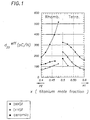
- Rhombohedral PZT also has a lower piezoelectric constant than tetragonal PZT ( Figure 1; Du, et al ., Appl. Phys. Lett. 72 :2421-2423, 1998).
- the minimum electromechanical coefficient, d 33 is significantly smaller along the pseudo-cubic [111] direction of the rhombohedral phase than along any direction in the tetragonal phase.
- the small dependence of the d 33 coefficient on composition provides the flexibility to choose the best composition for the ferroelectric material from an electrical performance standpoint.
- PbZr 1-x Ti x O 3 thin films where x is between 0.15 and 0.4, have a rhombohedral unit cell and are also far from the phase transition regions of rhombohedral to tetragonal (x ⁇ 0.5) and rhombohedral to orthogonal at x ⁇ 0.1.
- ferroelectric materials such as tetragonal PZT
- the 90 degree domains form in thin films to compensate for the thermal and lattice mistatch strain between the ferroelectric and the substrate, thereby reducing the system energy.
- Tetragonal PZT exhibits a strong polarization dipole along the [001] and virtually no polarization along the [100], which forms a 90 degree angle with [001] in tetragonal systems.
- These [100] domains cannot be electrically switched, yielding no switched charge.
- the switched charge per capacitor will vary according to the domain pattern in the films. As the transistor size decreases, the ferroelectric capacitor must be reduced to fit within a smaller area.
- the switched charge per capacitor encompasses fewer and fewer averaged domains.
- the average switched charge will decrease as 90 degree domains, which contribute no switched charge, are formed.
- the rhombohedral phase material has a similar behavior to the tetragonal material and forms domains at angles slightly lower than 90 degrees. However, unlike the tetragonal material, the maximum dipole moment of the rhombohedral material lies along the 111 direction.
- each domain will include a component, or projection, of [111], thereby reducing the variation in polarization charge between domains, yielding more consistent switched charge from one capacitor cell to another.
- Rhombohedral compositions of (100) PZT display remnant polarizations of approximately 40 ⁇ C/cm 2 and coercive fields of 25-30 kV/cm. Because the maximum dipole lies along [111] and measurements of (100) oriented materials only indicate projections of the maximum (vector) value, (111) oriented rhombohedral materials may yield even higher remnant polarizations (Foster, et al ., J . Appl . Phys . 81 :2349-2357, 1997).
- rhombohedral PZT is incorporated as a dielectric layer into a ferroelectric memory device.
- Figure 2 shows an exemplary one-transistor/one-capacitor ferroelectric memory device 10 comprising a silicon (or other semiconductor) substrate 12, transistor 14, plugs 16, a diffusion barrier 18, a bottom electrode 20, a dielectric layer 22, a top electrode 24, a bit line 26, and a metal line 28.
- a silicon (or other semiconductor) substrate 12 transistor 14
- plugs 16 a diffusion barrier 18
- bottom electrode 20 a dielectric layer 22
- top electrode 24 a bit line 26
- a metal line 28 a metal line 28.
- Rhombohedral PZT can also be incorporated into one-transistor type memories such as those described by U.S. Patent No. 3,832,700 to Wu, the entire contents of which are incorporated herein by reference.
- Rhombohedral PZT films can be deposited via metal-organic chemical vapor deposition (MOCVD), sputtering, or sol-gel.
- MOCVD metal-organic chemical vapor deposition
- the phase is controlled in part by controlling the composition of the precursor materials.
- the grain size and orientation of a film deposited through any of these techniques may be engineered by any of several mechanisms.
- film texture is controlled by selecting a template having an interatomic spacing similar to the spacing of the desired lattice plane parallel to the substrate. Thus, if the lattice constants of the template and the growing film are similar, a particular growth direction can be promoted by obtaining a particular orientation in the substrate.
- This principle may be applied to the deposition of PZT films by using either platinum or iridium as the template. Platinum and iridium are commonly used as electrodes for ferroelectric capacitors, and it is fortuitous that their lattice constants are particularly suited to this application.
- the substrate is not necessarily limited to Pt or Ir. Other applications for these oriented ferroelectric films may require different substrates. The only requirement is that the substrate have some plane (hkl) where the interatomic spacing is compatible with the interatomic spacing of the desired plane (h'k'l') along which the deposited material is being deposited. That is, the interatomic spacing of the substrate should facilitate film growth in the desired orientation. A general rule of thumb is that the two interatomic spacings should differ by less than about 10%.
- the lattice constants of iridium and platinum are approximately 0.394 nm and 0.392 nm, while rhombohedral PZT has a lattice constant of ⁇ 0.41 nm.
- the lattice constants in the (111) direction for Ir and Pt are 0.653 nm and 0.680 nm; PZT (111) has a lattice constant of 0.71187 nm.
- the lattice mismatch between either Ir or Pt with the PZT is less than about 8%.
- PZT grown on (100) or (111) Pt or Ir would be expected to exhibit (100) or (111) texturing, respectively.
- (100) is the fast growing plane. Intermediate growth temperatures ( ⁇ 400°C) and relatively high deposition rates will encourage growth of (100) Pt.
- the (111) plane is the low energy surface; therefore, higher temperatures (>400°C) that yield low growth rates will encourage this orientation.
- Another mechanism for encouraging (111) oriented Pt is to add a thin Ti seed layer beneath the Pt. It is well documented experimentally that Ti seed layers encourage a (111) texture.
- PZT layers for capacitors are frequently deposited on single crystal substrates
- other surfaces on which the PZT layers are deposited e.g., for transistors
- closely matched lattice constants are not sufficient to ensure development of the desired texture.
- Careful control of the deposition conditions and exploitation of other physical properties of the materials system may encourage a particular crystallographic orientation.
- a third mechanism for controlling the texture is to adjust the deposition temperature of the PZT thin film in a similar manner to that described above for Pt and Ir.
- the (111) orientation of the PZT can be promoted through lower growth rates at higher temperatures.
- the ferroelectric dipole lies along the [111] direction. This may further encourage the (111) growth orientation.
Landscapes
- Chemical & Material Sciences (AREA)
- Inorganic Chemistry (AREA)
- General Chemical & Material Sciences (AREA)
- Chemical Kinetics & Catalysis (AREA)
- Engineering & Computer Science (AREA)
- Materials Engineering (AREA)
- Mechanical Engineering (AREA)
- Metallurgy (AREA)
- Organic Chemistry (AREA)
- Semiconductor Memories (AREA)
- Compositions Of Oxide Ceramics (AREA)
- Physical Vapour Deposition (AREA)
- Chemical Vapour Deposition (AREA)
Abstract
Description
Claims (11)
- An apparatus having a multi-layer electrical device, comprising:a dielectric layer (22); andan electrically conductive layer (24) in electrical communication with the dielectric layer (22), whereinthe dielectric layer (22) comprises a piezoelectric material,the composition and orientation of the dielectric layer (22) are chosen to minimize the effect of the mechanical stresses imposed by the other layers of the device on the electrical properties of the piezoelectric material in the dielectric layer (22), anda number of domains in the dielectric layer (22) which are oriented along a projection of a polarization dipole of the piezoelectric material is maximized.
- An apparatus having an oriented thin film comprising a dielectric material (22), whereincharacteristics of the film have been optimized to minimize the interaction between voltage across the dielectric material and mechanical stress on the dielectric material,the optimized characteristics are selected from the group consisting of the composition of the dielectric material and the orientation of the film, andthe dielectric material comprises a piezoelectric material.
- The apparatus of claim 1, wherein the electrically conductive layer (24) is adjacent to the dielectric layer.
- The apparatus of claim 1 or 2, wherein the piezoelectric material comprises a ferroelectric material.
- The apparatus of claim 4, wherein the ferroelectric material has the composition PbZr1-xTixO3, wherein 0.15<x<0.4.
- The apparatus of claim 5, wherein the PbZr1-xTixO3 has a (111) orientation.
- The apparatus of claim 5, wherein the PbZr1-xTixO3 has a rhombohedral unit cell.
- The apparatus of claim 5, wherein the the PbZr1-xTixO3 is deposited on an underlying layer (20) having an interatomic spacing compatible with that of the interatomic spacing within a plane with respect to which the deposited PbZr1-xTixO3 is to be oriented.
- The apparatus of claim 8, wherein the substrate material (20) comprises a material having an interatomic spacing between 0.37 and 0.45 nm, platinum, or iridium.
- The apparatus of claim 1, wherein the device is a transistor or a capacitor.
- An electrical device comprising a ferroelectric thin film, wherein:the thin film comprises PbZr1-xTixO3 having a rhombohedral unit cell;
andthe thin film has a (111) orientation.
Applications Claiming Priority (2)
| Application Number | Priority Date | Filing Date | Title |
|---|---|---|---|
| US570185 | 2000-05-12 | ||
| US09/570,185 US6396094B1 (en) | 2000-05-12 | 2000-05-12 | Oriented rhombohedral composition of PbZr1-xTixO3 thin films for low voltage operation ferroelectric RAM |
Publications (2)
| Publication Number | Publication Date |
|---|---|
| EP1160870A2 true EP1160870A2 (en) | 2001-12-05 |
| EP1160870A3 EP1160870A3 (en) | 2005-06-15 |
Family
ID=24278604
Family Applications (1)
| Application Number | Title | Priority Date | Filing Date |
|---|---|---|---|
| EP01110358A Withdrawn EP1160870A3 (en) | 2000-05-12 | 2001-04-26 | Oriented rhombohedral composition of PbZr1-xTix03 thin films for low voltage operation ferroelectric ram |
Country Status (3)
| Country | Link |
|---|---|
| US (1) | US6396094B1 (en) |
| EP (1) | EP1160870A3 (en) |
| JP (1) | JP2002076295A (en) |
Cited By (3)
| Publication number | Priority date | Publication date | Assignee | Title |
|---|---|---|---|---|
| EP1229569A2 (en) | 2001-01-31 | 2002-08-07 | Fujitsu Limited | Capacitor semiconductor device comprising the same and method of fabricating thereof |
| EP1675162A3 (en) * | 2004-12-27 | 2007-05-30 | Seiko Epson Corporation | Ferroelectric film, method of manufacturing ferroelectric film, ferroelectric capacitor, and ferroelectric memory |
| EP1587146A3 (en) * | 2004-04-15 | 2007-05-30 | Seiko Epson Corporation | Metal thin film and method of manufacturing the same, dielectric capacitor and method of manufacturing the same, and semiconductor memory device |
Families Citing this family (8)
| Publication number | Priority date | Publication date | Assignee | Title |
|---|---|---|---|---|
| US6728093B2 (en) * | 2002-07-03 | 2004-04-27 | Ramtron International Corporation | Method for producing crystallographically textured electrodes for textured PZT capacitors |
| JP2004165351A (en) * | 2002-11-12 | 2004-06-10 | Fujitsu Ltd | Method for manufacturing semiconductor device |
| JP4507491B2 (en) * | 2002-12-27 | 2010-07-21 | セイコーエプソン株式会社 | Thin film and element |
| EP1585176A4 (en) * | 2003-01-17 | 2007-10-03 | Fujitsu Ltd | FERROELECTRIC CAPACITOR AND METHOD FOR PRODUCING THE SAME |
| US20050199924A1 (en) * | 2004-03-10 | 2005-09-15 | Fox Glen R. | Optimized ferroelectric material crystallographic texture for enhanced high density feram |
| JP4548597B2 (en) * | 2005-03-25 | 2010-09-22 | セイコーエプソン株式会社 | Piezoelectric element manufacturing method, ink jet recording head manufacturing method, and ink jet printer manufacturing method |
| JP5064094B2 (en) * | 2007-04-16 | 2012-10-31 | パナソニック株式会社 | Semiconductor memory device and manufacturing method thereof |
| US9773793B2 (en) * | 2009-10-09 | 2017-09-26 | Texas Instuments Incorporated | Transistor performance modification with stressor structures |
Family Cites Families (14)
| Publication number | Priority date | Publication date | Assignee | Title |
|---|---|---|---|---|
| JPS58161924A (en) * | 1982-03-16 | 1983-09-26 | Agency Of Ind Science & Technol | Manufacture of transparent thin strip of crystalline oriented lanthanum niobate |
| JP2809718B2 (en) * | 1989-06-30 | 1998-10-15 | 株式会社東芝 | Ferroelectric memory |
| JPH03262174A (en) * | 1990-03-13 | 1991-11-21 | Nikko Kyodo Co Ltd | Oxide thin film device |
| JPH0463482A (en) * | 1990-07-03 | 1992-02-28 | Olympus Optical Co Ltd | Ferroelectric memory |
| JPH0575137A (en) * | 1991-09-17 | 1993-03-26 | Olympus Optical Co Ltd | Manufacture of ferroelectric memory |
| JPH0773732A (en) * | 1993-06-23 | 1995-03-17 | Sharp Corp | Dielectric thin film element and manufacturing method thereof |
| JP3681196B2 (en) * | 1995-03-31 | 2005-08-10 | Tdk株式会社 | Method for manufacturing ferroelectric thin film |
| JP3368726B2 (en) | 1995-08-07 | 2003-01-20 | ヤマハ株式会社 | Semiconductor memory device and manufacturing method thereof |
| US5719417A (en) * | 1996-11-27 | 1998-02-17 | Advanced Technology Materials, Inc. | Ferroelectric integrated circuit structure |
| US5815305A (en) * | 1997-03-10 | 1998-09-29 | Daewoo Electronics Co., Ltd. | Thin film actuated mirror array in an optical projection system and method for manufacturing the same |
| US6097135A (en) * | 1998-05-27 | 2000-08-01 | Louis J. Desy, Jr. | Shaped multilayer ceramic transducers and method for making the same |
| US6258459B1 (en) * | 1998-04-28 | 2001-07-10 | Tdk Corporation | Multilayer thin film |
| US6248394B1 (en) * | 1998-08-14 | 2001-06-19 | Agere Systems Guardian Corp. | Process for fabricating device comprising lead zirconate titanate |
| JP4327942B2 (en) * | 1999-05-20 | 2009-09-09 | Tdk株式会社 | Thin film piezoelectric element |
-
2000
- 2000-05-12 US US09/570,185 patent/US6396094B1/en not_active Expired - Fee Related
-
2001
- 2001-04-26 EP EP01110358A patent/EP1160870A3/en not_active Withdrawn
- 2001-05-11 JP JP2001140880A patent/JP2002076295A/en active Pending
Cited By (7)
| Publication number | Priority date | Publication date | Assignee | Title |
|---|---|---|---|---|
| EP1229569A2 (en) | 2001-01-31 | 2002-08-07 | Fujitsu Limited | Capacitor semiconductor device comprising the same and method of fabricating thereof |
| EP1229569A3 (en) * | 2001-01-31 | 2006-11-22 | Fujitsu Limited | Capacitor semiconductor device comprising the same and method of fabricating thereof |
| EP1587146A3 (en) * | 2004-04-15 | 2007-05-30 | Seiko Epson Corporation | Metal thin film and method of manufacturing the same, dielectric capacitor and method of manufacturing the same, and semiconductor memory device |
| CN100388497C (en) * | 2004-04-15 | 2008-05-14 | 精工爱普生株式会社 | Metal thin film, manufacturing method thereof, dielectric capacitor, manufacturing method thereof, and semiconductor device |
| US7425738B2 (en) | 2004-04-15 | 2008-09-16 | Seiko Epson Corporation | Metal thin film and method of manufacturing the same, dielectric capacitor and method of manufacturing the same, and semiconductor device |
| EP1675162A3 (en) * | 2004-12-27 | 2007-05-30 | Seiko Epson Corporation | Ferroelectric film, method of manufacturing ferroelectric film, ferroelectric capacitor, and ferroelectric memory |
| US7569400B2 (en) | 2004-12-27 | 2009-08-04 | Seiko Epson Corporation | Ferroelectric film, method of manufacturing ferroelectric film, ferroelectric capacitor, and ferroelectric memory |
Also Published As
| Publication number | Publication date |
|---|---|
| JP2002076295A (en) | 2002-03-15 |
| US6396094B1 (en) | 2002-05-28 |
| EP1160870A3 (en) | 2005-06-15 |
Similar Documents
| Publication | Publication Date | Title |
|---|---|---|
| CN111295735B (en) | Hafnium oxide and zirconium oxide based ferroelectric devices with textured iridium bottom electrodes | |
| Lu et al. | Enhancement of ferroelectric polarization stability by interface engineering | |
| JP3373525B2 (en) | Multilayer ferroelectric cell and perovskite electron heterostructure integrated on silicon | |
| US5760432A (en) | Thin film strained layer ferroelectric capacitors | |
| EP1229569B1 (en) | Capacitor, semiconductor device comprising the same and method of fabricating thereof | |
| US8022454B2 (en) | Ferroelectric thin films | |
| US6396094B1 (en) | Oriented rhombohedral composition of PbZr1-xTixO3 thin films for low voltage operation ferroelectric RAM | |
| US20100006953A1 (en) | Integrated circuit including a dielectric layer | |
| US6728093B2 (en) | Method for producing crystallographically textured electrodes for textured PZT capacitors | |
| JPH10270654A (en) | Semiconductor storage device | |
| US7071007B2 (en) | Method of forming a low voltage drive ferroelectric capacitor | |
| JPH10269842A (en) | Conductive oxide thin film, thin film capacitor and magnetoresistive element | |
| TWI272716B (en) | Metal thin film and method of manufacturing the same, dielectric capacitor and method of manufacturing the same, and semiconductor device | |
| WO2008050271A2 (en) | Ferroelectric varactor with improved tuning range | |
| Schneider et al. | Impact of strain engineering on antiferroelectricity in NaNbO3 thin films | |
| US6853535B2 (en) | Method for producing crystallographically textured electrodes for textured PZT capacitors | |
| US20080075980A1 (en) | Epitaxial ferroelectric and magnetic recording structures including graded lattice matching layers | |
| JP2002525876A (en) | Ferroelectric thin film with low tetragonality | |
| Nonomura et al. | Epitaxial growth and ferroelectric properties of the 20-nm-thick Pb (Zr, Ti) O3 film on SrTiO3 (100) with an atomically flat surface by metalorganic chemical vapor deposition | |
| Shin et al. | Tetragonally strained crystal structure and ferroelectric properties of epitaxial PbTiO3 thin films grown on single-crystal Rh substrates | |
| Lee et al. | Domain wall current, ferroelectric, and piezoelectric properties of flexible SrBi2Ta2O9 thin films affected by the distribution of a-oriented domains and c-oriented domains | |
| Wouters et al. | Ultra-thin PZT films for low-voltage ferroelectric non-volatile memories | |
| JPH1187634A (en) | Thin film capacitors | |
| US20220293766A1 (en) | Semiconducting Ferroelectric Device | |
| Lim et al. | Dependence of ferroelectric performance of sol–gel-derived Pb (Zr, Ti) O 3 thin films on bottom-Pt-electrode thickness |
Legal Events
| Date | Code | Title | Description |
|---|---|---|---|
| PUAI | Public reference made under article 153(3) epc to a published international application that has entered the european phase |
Free format text: ORIGINAL CODE: 0009012 |
|
| AK | Designated contracting states |
Kind code of ref document: A2 Designated state(s): AT BE CH CY DE DK ES FI FR GB GR IE IT LI LU MC NL PT SE TR |
|
| AX | Request for extension of the european patent |
Free format text: AL;LT;LV;MK;RO;SI |
|
| PUAL | Search report despatched |
Free format text: ORIGINAL CODE: 0009013 |
|
| AK | Designated contracting states |
Kind code of ref document: A3 Designated state(s): AT BE CH CY DE DK ES FI FR GB GR IE IT LI LU MC NL PT SE TR |
|
| AX | Request for extension of the european patent |
Extension state: AL LT LV MK RO SI |
|
| 17P | Request for examination filed |
Effective date: 20050728 |
|
| AKX | Designation fees paid |
Designated state(s): DE FR GB |
|
| RAP1 | Party data changed (applicant data changed or rights of an application transferred) |
Owner name: AVAGO TECHNOLOGIES GENERAL IP (SINGAPORE) PTE. LTD |
|
| STAA | Information on the status of an ep patent application or granted ep patent |
Free format text: STATUS: THE APPLICATION IS DEEMED TO BE WITHDRAWN |
|
| 18D | Application deemed to be withdrawn |
Effective date: 20071101 |