EP1160867A2 - Electronic circuit unit that is suitable for miniaturization and excellent in high frequency charateristic - Google Patents
Electronic circuit unit that is suitable for miniaturization and excellent in high frequency charateristic Download PDFInfo
- Publication number
- EP1160867A2 EP1160867A2 EP01304504A EP01304504A EP1160867A2 EP 1160867 A2 EP1160867 A2 EP 1160867A2 EP 01304504 A EP01304504 A EP 01304504A EP 01304504 A EP01304504 A EP 01304504A EP 1160867 A2 EP1160867 A2 EP 1160867A2
- Authority
- EP
- European Patent Office
- Prior art keywords
- bare chip
- electrode
- capacitor
- electronic circuit
- semiconductor bare
- Prior art date
- Legal status (The legal status is an assumption and is not a legal conclusion. Google has not performed a legal analysis and makes no representation as to the accuracy of the status listed.)
- Withdrawn
Links
Images




Classifications
-
- H—ELECTRICITY
- H05—ELECTRIC TECHNIQUES NOT OTHERWISE PROVIDED FOR
- H05K—PRINTED CIRCUITS; CASINGS OR CONSTRUCTIONAL DETAILS OF ELECTRIC APPARATUS; MANUFACTURE OF ASSEMBLAGES OF ELECTRICAL COMPONENTS
- H05K1/00—Printed circuits
- H05K1/18—Printed circuits structurally associated with non-printed electric components
-
- H—ELECTRICITY
- H05—ELECTRIC TECHNIQUES NOT OTHERWISE PROVIDED FOR
- H05K—PRINTED CIRCUITS; CASINGS OR CONSTRUCTIONAL DETAILS OF ELECTRIC APPARATUS; MANUFACTURE OF ASSEMBLAGES OF ELECTRICAL COMPONENTS
- H05K3/00—Apparatus or processes for manufacturing printed circuits
- H05K3/40—Forming printed elements for providing electric connections to or between printed circuits
- H05K3/403—Edge contacts; Windows or holes in the substrate having plural connections on the walls thereof
-
- H—ELECTRICITY
- H10—SEMICONDUCTOR DEVICES; ELECTRIC SOLID-STATE DEVICES NOT OTHERWISE PROVIDED FOR
- H10W—GENERIC PACKAGES, INTERCONNECTIONS, CONNECTORS OR OTHER CONSTRUCTIONAL DETAILS OF DEVICES COVERED BY CLASS H10
- H10W44/00—Electrical arrangements for controlling or matching impedance
- H10W44/20—Electrical arrangements for controlling or matching impedance at high-frequency [HF] or radio frequency [RF]
-
- H—ELECTRICITY
- H05—ELECTRIC TECHNIQUES NOT OTHERWISE PROVIDED FOR
- H05K—PRINTED CIRCUITS; CASINGS OR CONSTRUCTIONAL DETAILS OF ELECTRIC APPARATUS; MANUFACTURE OF ASSEMBLAGES OF ELECTRICAL COMPONENTS
- H05K1/00—Printed circuits
- H05K1/02—Details
- H05K1/03—Use of materials for the substrate
- H05K1/0306—Inorganic insulating substrates, e.g. ceramic, glass
-
- H—ELECTRICITY
- H05—ELECTRIC TECHNIQUES NOT OTHERWISE PROVIDED FOR
- H05K—PRINTED CIRCUITS; CASINGS OR CONSTRUCTIONAL DETAILS OF ELECTRIC APPARATUS; MANUFACTURE OF ASSEMBLAGES OF ELECTRICAL COMPONENTS
- H05K1/00—Printed circuits
- H05K1/02—Details
- H05K1/09—Use of materials for the conductive, e.g. metallic pattern
- H05K1/092—Dispersed materials, e.g. conductive pastes or inks
-
- H—ELECTRICITY
- H05—ELECTRIC TECHNIQUES NOT OTHERWISE PROVIDED FOR
- H05K—PRINTED CIRCUITS; CASINGS OR CONSTRUCTIONAL DETAILS OF ELECTRIC APPARATUS; MANUFACTURE OF ASSEMBLAGES OF ELECTRICAL COMPONENTS
- H05K2201/00—Indexing scheme relating to printed circuits covered by H05K1/00
- H05K2201/03—Conductive materials
- H05K2201/0302—Properties and characteristics in general
- H05K2201/0317—Thin film conductor layer; Thin film passive component
-
- H—ELECTRICITY
- H05—ELECTRIC TECHNIQUES NOT OTHERWISE PROVIDED FOR
- H05K—PRINTED CIRCUITS; CASINGS OR CONSTRUCTIONAL DETAILS OF ELECTRIC APPARATUS; MANUFACTURE OF ASSEMBLAGES OF ELECTRICAL COMPONENTS
- H05K2201/00—Indexing scheme relating to printed circuits covered by H05K1/00
- H05K2201/03—Conductive materials
- H05K2201/0332—Structure of the conductor
- H05K2201/0335—Layered conductors or foils
- H05K2201/0347—Overplating, e.g. for reinforcing conductors or bumps; Plating over filled vias
-
- H—ELECTRICITY
- H05—ELECTRIC TECHNIQUES NOT OTHERWISE PROVIDED FOR
- H05K—PRINTED CIRCUITS; CASINGS OR CONSTRUCTIONAL DETAILS OF ELECTRIC APPARATUS; MANUFACTURE OF ASSEMBLAGES OF ELECTRICAL COMPONENTS
- H05K3/00—Apparatus or processes for manufacturing printed circuits
- H05K3/22—Secondary treatment of printed circuits
- H05K3/24—Reinforcing of the conductive pattern
- H05K3/245—Reinforcing conductive patterns made by printing techniques or by other techniques for applying conductive pastes, inks or powders; Reinforcing other conductive patterns by such techniques
- H05K3/246—Reinforcing conductive paste, ink or powder patterns by other methods, e.g. by plating
-
- H—ELECTRICITY
- H10—SEMICONDUCTOR DEVICES; ELECTRIC SOLID-STATE DEVICES NOT OTHERWISE PROVIDED FOR
- H10W—GENERIC PACKAGES, INTERCONNECTIONS, CONNECTORS OR OTHER CONSTRUCTIONAL DETAILS OF DEVICES COVERED BY CLASS H10
- H10W72/00—Interconnections or connectors in packages
- H10W72/071—Connecting or disconnecting
- H10W72/075—Connecting or disconnecting of bond wires
-
- H—ELECTRICITY
- H10—SEMICONDUCTOR DEVICES; ELECTRIC SOLID-STATE DEVICES NOT OTHERWISE PROVIDED FOR
- H10W—GENERIC PACKAGES, INTERCONNECTIONS, CONNECTORS OR OTHER CONSTRUCTIONAL DETAILS OF DEVICES COVERED BY CLASS H10
- H10W72/00—Interconnections or connectors in packages
- H10W72/851—Dispositions of multiple connectors or interconnections
- H10W72/874—On different surfaces
- H10W72/884—Die-attach connectors and bond wires
-
- H—ELECTRICITY
- H10—SEMICONDUCTOR DEVICES; ELECTRIC SOLID-STATE DEVICES NOT OTHERWISE PROVIDED FOR
- H10W—GENERIC PACKAGES, INTERCONNECTIONS, CONNECTORS OR OTHER CONSTRUCTIONAL DETAILS OF DEVICES COVERED BY CLASS H10
- H10W72/00—Interconnections or connectors in packages
- H10W72/90—Bond pads, in general
- H10W72/951—Materials of bond pads
-
- H—ELECTRICITY
- H10—SEMICONDUCTOR DEVICES; ELECTRIC SOLID-STATE DEVICES NOT OTHERWISE PROVIDED FOR
- H10W—GENERIC PACKAGES, INTERCONNECTIONS, CONNECTORS OR OTHER CONSTRUCTIONAL DETAILS OF DEVICES COVERED BY CLASS H10
- H10W90/00—Package configurations
- H10W90/701—Package configurations characterised by the relative positions of pads or connectors relative to package parts
- H10W90/751—Package configurations characterised by the relative positions of pads or connectors relative to package parts of bond wires
- H10W90/754—Package configurations characterised by the relative positions of pads or connectors relative to package parts of bond wires between a chip and a stacked insulating package substrate, interposer or RDL
Definitions
- This invention relates to a surface mounting type electronic circuit unit on which a semiconductor bare chip and a capacitor are mounted, and particularly relates to an electronic circuit unit that is suitably used as a high frequency device.
- an electronic circuit unit used as a high frequency device is fabricated by soldering various circuit parts such as chip resistors and chip capacitors on soldering land of conducting patterns formed on a substrate.
- a small-sized electronic circuit unit fabricated by forming thin film circuit elements on a substrate by means of thin film forming technique has been developed with recent progress of integrated circuit fabrication technology.
- a method is employed in which a plurality of thin film capacitors and a wiring pattern are formed on a substrate by means of thin film forming technique and a transistor bare chip is mounted and wire-bonded on a substrate.
- the thin film capacitor is formed by laminating a bottom electrode, a dielectric layer, and a top electrode successively, and a part of a wiring pattern is served as the bottom electrode and top electrode.
- the bottom side collector electrode of a transistor is connected to a connection land with conductive adhesive
- the top side emitter electrode and base electrode are connected to a bonding pad with a wire
- the wiring pattern is served also as the connection land and bonding pad.
- the electronic circuit unit can be miniaturized to some extent because at least a plurality of capacitors are formed on a substrate by means of thin film forming technique, however, because a plurality of capacitors and wiring patterns are formed in the limited area on a substrate by means of thin film forming technique, it is difficult to miniaturize the electronic circuit unit further.
- an electronic circuit unit of this type has an amplifier circuit and the emitter of a transistor used as an amplifier circuit is grounded through a capacitor
- a method in which the bottom electrode or top electrode of a thin film capacitor is connected to a bonding pad through a wiring pattern and the emitter electrode is connected to the bonding pad by means of wire bonding has been employed in the above-mentioned conventional art.
- This method is disadvantageous because the high frequency characteristic can be poor due to the inductance of the wiring pattern interposed between the thin film capacitor and bonding pad.
- the present invention has been accomplished in view of the problem of the conventional art, and it is the object of the present invention to provide an electronic circuit unit that is suitable for miniaturization and excellent in high frequency characteristic.
- an electronic circuit unit of the present invention comprises a conducting pattern formed on an alumina substrate by means of thin film forming technique, circuit elements including capacitors, resistors, and inductance elements formed on the alumina substrate by means of thin film forming technique so as to be connected to the conducting pattern, and a semiconductor bare chip fixed to the conductive pattern by means of wire bonding, wherein the area of the connection land on which the semiconductor bare chip is mounted is smaller than the bottom surface area of the semiconductor bare chip.
- circuit elements including capacitors, resistors, and inductance elements are formed with high precision by means of thin film forming technique and a semiconductor bare chip is fixed by means of wire bonding, necessary circuit parts are mounted in high density on an alumina substrate and a surface mounting type electronic circuit unit that is suitable for miniaturization is realized. Furthermore, because the area of the connection land on which the semiconductor bare chip is mounted is smaller than the bottom surface area of the semiconductor bare chip, conductive adhesive applied on the connection land such as cream solder or conducting paste can be retained inside the contour of the semiconductor bare chip, and it is prevented that the conductive adhesive spews from the contour of the semiconductor bare chip to result in short-circuit to the surrounding conducting pattern.
- connection land it is desirable that an opening is formed in the connection land. Thereby, the excessive conductive adhesive can be retained in the opening, and spewing of the conductive adhesive is more surely prevented.
- an electronic circuit unit of the present invention has the structure in which a capacitor is formed by laminating a bottom electrode and top electrode with interposition of a dielectric material on a substrate, and a semiconductor bare chip is mounted so as to be located on the capacitor on the substrate, wherein the top electrode of the capacitor is served as a part of a connection land connected to the bottom side electrode of the semiconductor bare chip.
- the thin film capacitor is formed just under the space where the semiconductor bare chip is mounted, the areal efficiency of the substrate is improved because the semiconductor bare chip and thin capacitor are placed one on the other, and the electronic circuit unit made even more small-sized. Furthermore, because the top electrode of the thin film capacitor is served also as a part of the connection land that is connected to the bottom side electrode of the semiconductor bare chip, the lead inductance component between the thin film capacitor and the semiconductor bare chip is reduced, and the deterioration of high frequency characteristic is prevented.
- the electronic circuit unit of the present invention has the structure in which a capacitor is formed by laminating a bottom electrode and a top electrode with interposition of a dielectric material on a substrate, and a semiconductor bare chip is mounted on the substrate, wherein the top electrode of the capacitor is connected to the top side electrode of the semiconductor bare chip by means of wire bonding.
- the top side electrode of the semiconductor bare chip is wire-bonded by use of the top electrode of the thin film capacitor as a bonding pad, the areal efficiency of the substrate is improved by the area corresponding to the bonding pad, and the electronic circuit unit can be further miniaturized. Furthermore, because the top electrode of the thin film capacitor is served also as the bonding pad that is wire-bonded to the top side electrode of the semiconductor bare chip, the lead inductance between the thin film capacitor and the semiconductor bare chip is reduced, and the deterioration of high frequency characteristic is prevented.
- FIG. 1 is a perspective view of an electronic circuit unit
- FIG. 2 is a plan view of an alumina substrate illustrating the circuit structure layout
- FIG. 3 is a backside view of the alumina substrate
- FIG. 4 is an explanatory view of the circuit structure
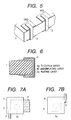
- FIG. 5 is a perspective view illustrating end side electrodes
- FIG. 6 is a cross sectional view of an end side electrode
- FIG. 7A and FIG. B are explanatory views illustrating the relation between a semiconductor bare chip and a connection land
- FIG. 8A to FIG. 8J are explanatory views illustrating a fabrication process of an electronic circuit unit.
- the present embodiment is an example in which the present invention is applied to a frequency tuning type booster amplifier, the frequency tuning type booster amplifier is used for improving the reception performance (particularly for improvement of the reception sensitivity and anti-disturbance characteristic) of a potable type television apparatus in combination with a UHF tuner. Thereby, a TV signal of a desired frequency is selected, and the selected TV signal is amplified and supplied to the UHF tuner.
- FIG. 1 shows an apparent configuration of such frequency tuning type booster amplifier (electronic circuit unit).
- the frequency tuning type booster amplifier comprises an alumina substrate 1 on which circuit component elements are mounted, that will be described hereinafter, and a shield cover 2 fixed to the alumina substrate 1.
- the frequency tuning type booster amplifier will be used as a surface mounting parts that is to be soldered to a mother substrate not shown in the drawing.
- the alumina substrate 1 is configured in a rectangular flat plate, which is obtained by cutting a large substrate into divided rectangles and by dividing a divided rectangle further into small pieces.
- the shield cover 2 is formed by bending a metal plate into a box, and the circuit component element on the alumina substrate 1 is covered by the shield cover 2.
- the circuit component elements and a conducting pattern that is served to connect the circuit component elements are provided on the surface of the alumina substrate 1, and as shown in FIG. 3, a conducting pattern that is served as a backside electrode is provided on the backside of the alumina substrate 1.
- the frequency tuning type booster amplifier in accordance with the present embodiment having the circuit structure as shown in FIG. 4 is provided with a tuning circuit and amplifier circuit for selecting a TV signal and amplification respectively, and the same characters of the circuit diagram shown in FIG. 4 are given to the same circuit component elements shown in FIG. 2.
- FIG. 4 shows only an example of the circuit structure, and the present invention is applied to other electronic circuit units having the circuit structure different from the above-mentioned circuit structure.
- the frequency tuning type booster amplifier has capacitors C1 to C7, resistors R1 to R3, inductance elements L1 to L3, a diode D1, a transistor Tr1, and conducting paths S1 and S2 that are served as the circuit component element of the tuning circuit and amplifier circuit, and these circuit component elements and the conducting pattern are provided on the surface of the alumina substrate 1.
- the conducting pattern is formed of, for example, Cr or Cu by means of thin film forming technique such as spattering, and is shown with hatching having a character P in FIG. 2.
- the frequency tuning type booster amplifier is provided with the tuning circuit comprising inductance elements L2 and L3, capacitors C3 and C4, and the diode D1 and the amplifier circuit comprising the transistor Tr1, peripheral circuit elements (resistors R1 to R3, capacitor C6), and a unbalance/balance conversion element T to select and amplify a TV signal of a desired frequency.
- the TV signal of a plurality of frequencies is supplied to the tuning circuit through the capacitor C1.
- the tuning frequency (resonance frequency) of the tuning circuit is variable by controlling a voltage (Vct1) applied on the cathode of the diode D1, only the desired TV signal is selected by adjusting the tuning frequency to the frequency of the desired TV signal, and the TV signal is supplied to the base of the transistor Tr1 of the amplifier circuit through the capacitor C5.
- Bias voltages are applied to base bias voltage dividing resistances R1 and R2 of the base of the transistor Tr1, and the collector current ( ⁇ emitter current) of the transistor Tr1 is set depending on the resistance value of the emitter resistance R3.
- the TV signal that has been amplified by means of the transistor Tr1 is sent out from the collector where the unbalance/balance conversion element T is provided.
- the unbalance/balance conversion element T has an inductance element comprising a pair of conducting paths S1 and S2 that are combined together.
- the balance TV signal is generated from both ends of the conducting path S2, and supplied to the above-mentioned UHF tuner.
- ground electrodes (GND) and input electrodes (Vcc, Vctl, and RFin) and output electrodes (RFout) are formed on the ends of the alumina substrate 1, the conducting pattern P is partially served as these electrodes.
- the ground electrodes, input electrodes, and output electrodes are formed only on two longer sides of the rectangular alumina substrate 1 that are facing each other and are not formed on the two shorter sides that are facing each other.
- GND electrodes are formed on both corners of one longer side of the alumina substrate 1, and a Vcc electrode, an RFin electrode, and a Vctl electrode are formed between these GND electrodes.
- Three GND electrodes are formed on both corners of the other longer side of the alumina substrate 1 and near one corner, and two RFout electrodes are formed between these GND electrodes.
- the two longer sides of the alumina substrate 1 correspond to the parting line used when a large substrate is cut into divided rectangles
- the two shorter sides of the alumina substrate 1 correspond to the parting line used when a divided rectangle is further divided into small pieces.
- the conducting pattern P1 (backside electrode) formed on the back side of the alumina substrate 1 is facing to the ground electrodes (GND), input electrodes (Vcc, Vctl, and RFin), and output electrodes (RFout), and corresponding electrodes are rendered conductive through side end electrodes 3 as shown in FIG. 5 and FIG. 6.
- An end electrode 3 is formed by plating an Ni under layer and an Au layer successively on an Ag thick-film layer.
- the undermost thick film Ag layer has been formed by forming a thick film of Ag paste containing no glass composition and then by sintering it at a temperature of approximately 200 °C. Therefore, the undermost thick film Ag layer is formed of low temperature sintered material.
- the Ni under layer laminated in-between is served for firm adhering of the Au plating layer, and the uppermost Au plating layer is served for preventing deposition of Ag of the undermost layer on solder when the end side electrode 3 is soldered to a soldering land of a mother substrate not shown in the drawing.
- legs 2a formed by bending the shield cover 2 on the side are soldered to the end side electrodes 3 that are conductive to the ground electrodes (GND), and the shield cover 2 is grounded at the four corners of the alumina substrate 1.
- Each of the capacitors C1 to C7 among the above-mentioned circuit component elements is formed by laminating a top electrode on a bottom electrode with interposition of a film of dielectric material such as SiO 2 , and these thin films are formed by means of spattering.
- a Cu layer is formed on the surface of the top electrode and the Cu layer is effective to improve Q of the resonance circuit.
- the top electrode and the bottom electrode of each of the capacitors C1 to C7 is connected to the conducting pattern P, and discharging neighboring gaps (air gap) G are formed between the capacitor C7 and the Vcc electrode on the conducting pattern P, between the capacitor C7 and the RFout electrode on the conducting pattern P, and between the capacitor C2 and the Vctl electrode on the conducting pattern P.
- Each of these neighboring gaps G is formed of a pair of projections provided on the parallel conducting patterns P facing each other, and the tips of both projections are facing each other with interposition of a certain gap.
- the dimensional precision of the conducting pattern P and the GND electrode is very high because of the thin film forming technique, the gap dimensional size of the neighboring gap can be made very small, and discharging can occur at a low voltage.
- the capacitors C1 to C7 the capacitors C1 and C3 to C5 are formed simply rectangular, but the capacitors C2 and C7 are formed complexly non-rectangular with combination of two or more rectangles.
- the capacitor C2 has a concave shape having two rectangles projected from one side of another rectangle
- the capacitor C7 has a shape formed by three rectangles that are located continuously with a deviation in the longitudinal direction successively.
- These capacitors C2 and C7 are served as the ground capacitor for which a relatively large capacitance value is required, the ground capacitors C2 and C7 are formed complexly non-rectangular as described hereinabove because the limited space on the alumina substrate 1 is effectively used, and the capacitor of a desired capacitance value can be mounted in high density.
- the capacitor C6 comprises two ground capacitors having difference capacitance values, and the two capacitors are connected in parallel with interposition of a pair of conducting pattern P that are separated from each other.
- one electrode of each of both ground capacitors C6 is connected to the ground conducting pattern P connected to the GND electrode, and the other electrode of each of both ground capacitors C6 is connected to a connection land SL of the transistor Tr1 with interposition of the two conducting patterns P that are separated from each other.
- the capacitor C6 is located between the emitter of the transistor Tr1 and the ground, and the above-mentioned connection land SL is the portion where the emitter electrode of the transistor Tr1 is subjected to wire bonding. Therefore, the capacitance value of the capacitor C6 is set by two ground capacitors connected in parallel with interposition of the conducting patterns P that are separated from each other. As the result, the inductance of the whole conducting patterns P extending from the emitter electrode of the transistor Tr1 to the ground with interposition of the capacitor C6 is reduced, and the grounding effect of the connection land SL that is brought about by means of the ground capacitor C6 is improved. Furthermore, the parasitic oscillation frequency due to the ground capacitors C6 and conducting patterns P becomes higher. Therefore, the parasitic oscillation is prevented by setting the frequency to a value equal to or higher than the operating point frequency of the transistor Tr1.
- the resistors R1 to R3 are resistance films formed of, for example, TaSiO 2 by means of thin film forming technique such as spattering, and a film of dielectric material such as SiO 2 is formed on the surface of a resistor as required. As shown in FIG. 2, the resistors R1 and R2 among the three film resistors R1 to R3 are located adjacently in parallel each other on the alumina substrate 1, and another film resistor R3 is located apart from the resistors R1 and R2. Because the film resistors R1 and R2 are formed adjacently, the ratio of the whole dispersion of the resistors R1 and R2 can be equalized even though the resistance value of the resistors R1 and R2 deviates from the desired value.
- the resistors R1 and R2 are served as the base bias voltage dividing resistor of the transistor Tr1, a voltage of R1/ (R1+R2) ⁇ Vcc is applied on the base of the transistor Tr1.
- the resistor R3 is the emitter resistance of the transistor Tr1, and a current flows from the Vcc electrode to the collector and emitter of the transistor Tr1 and is grounded through the resistor R3. Because the contribution of the resistor R3 to the amplification of the transistor Tr1 is largest among the resistors R1 to R3, only the resistor R3 is trimmed so that the current value is made constant for output adjustment.
- the thin film resistors R1, R2, and R4 that are served as the base bias voltage dividing resistor of both transistors Tr1 and Tr2 are formed adjacently to each other on the alumina substrate 1, as the result trimming of the resistance value of the resistors R1, R2, and R4 is not required. Therefore, also in this case, the current value of both transistors Tr1 and Tr2 can be set by trimming only the resistor R3 that is served as the emitter resistance.
- the inductance elements L1 to L3 and the conducting paths S1 and S2 are formed of Cr or Cu by means of thin film forming technique such as spattering, and connected to the conducting pattern P.
- a Cu layer is formed on each of the inductance elements L1 to L3, and the Cu layer is effective to increase Q of a resonance circuit.
- Each of the inductance elements L1 and L2 is formed rectangularly swirlingly, and one end of each of the inductance elements L1 and L2 is wire-bonded to the Vctl electrode or ground conducting pattern P.
- the inductance element L2 is served to roughly set the resonance frequency, and the inductance element L3 is connected to the other end of the inductance element L2.
- the inductance element L3 is an adjusting conducting pattern served to adjust the resonance frequency.
- the inductance element L3 is trimmed as shown in FIG. 2 with a broken line to thereby increase the number of turns of the inductance element L2, and as the result the resonance frequency is adjusted.
- the conductor width of the trimmed inductance element L3 is equalized to the conductor width of the inductance element L2 that is served for setting the resonance frequency, the characteristic impedance of the inductance element L2 is resultantly equalized to the characteristic impedance of the inductance element L3.
- the unbalance/balance conversion element T has the inductance element comprising the pair of conducting paths S1 and S2 combined, and these thin film conducting paths S1 and S2 are formed on the alumina substrate 1.
- These conducting paths S1 and S2 are formed swirlingly on the alumina substrate 1 facing each other with interposition of a predetermined gap, both ends of the one conducting path S1 are connected to the collector electrode of the transistor Tr1 and the conducting pattern P connected to the capacitor C7, and both ends of the other conducting path S2 are connected to a pair of RFout electrodes.
- the gap between both conducting paths S1 and S2 can be made narrow and the desired sufficient coupling can be secured resultantly, and the small unbalance/balance conversion element T is disposed on a limited space on the alumina substrate 1.
- the pair of conducting paths S1 and S2 facing each other with interposition of the predetermined gap may be formed in zigzag fashion on the alumina substrate 1.
- the diode D1 and transistor Tr1 are formed by means of a process in which a semiconductor bare chip is mounted on the connection land of the thin film conducting pattern P formed on the alumina substrate 1 and the semiconductor bare chip is connected to the conducting pattern P by means of wire bonding.
- the semiconductor bare chip of the diode D1 is formed rectangular, the one electrode disposed on the bottom surface of the semiconductor bare chip is fixed to the connection land by use of conductive adhesive such as cream solder or conductive paste, and the other electrode disposed on the top surface of the semiconductor bare chip is connected to the predetermined position on the conducting pattern P by means of wire bonding.
- the semiconductor bare chip of the transistor Tr1 is formed also rectangular, the collector electrode disposed on the bottom surface of the semiconductor bare chip is fixed to the connection land by use of conductive adhesive, and the base electrode and the emitter electrode are connected to the predetermined position on the conducting pattern P by means of wire bonding.
- an Ni underplating layer and an Au plating layer are laminated successively on each of these connection lands.
- the connection land 5 is formed so that the area of the connection land 5 is smaller than the bottom surface area of the semiconductor bare chip 4, and a space for retaining conductive adhesive is secured under the semiconductor bare chip 4 because of such a structure.
- the space does not allow conductive adhesive from spewing outside the semiconductor bare chip 4 to result in short-circuit to the surrounding conducting pattern P. Furthermore, an opening 5a is formed in the connection land 5 and excessive conducting adhesive is retained in the opening 5a. Therefore, spewing of conductive adhesive is more surely prevented.
- a TaSiO 2 film is formed on the entire surface of an alumina substrate 1 by means of spattering and then etched in desired configuration to form a resistance film 6. Thereby, portions corresponding to the resistors R1 to R3 are formed.
- Cr film or Cu film is formed on the resistance film 6 by means of spattering and then etched in desired configuration to form the bottom electrode 7.
- a SiO 2 film is formed on the bottom electrode 7 by means of spattering and then etched in desired configuration to form the dielectric film 8.
- a Cr film or Cu film is formed on the dielectric film 8 by means of spattering and then etched in desired configuration to form the top electrode 9.
- the area corresponding to the conducting pattern P, inductance elements L1 to L3, and conducting paths S1 and S2 is formed by the bottom electrode 7 or the top electrode 9, and the area corresponding to the capacitors C1 to C7 is formed by the laminate comprising the bottom electrode 7, dielectric film 8, and top electrode 9.
- a Cu layer is formed on the surface of the area corresponding to the inductance elements L1 to L3, conducting paths S1 and S2, and capacitors C1 to C7 by means of plating or thin film forming technique, and a protecting film 10 is formed on the area excluding the area of the conducting pattern P as shown in FIG. 8E.
- a Cr film or Cu film is formed on the entire back surface of the alumina substrate 1 by means of spattering, and then etched in desired configuration to form the backside electrode 11. Thereby, the area corresponding to the backside conducting pattern P1 is formed.
- Steps described with reference to FIG. 8A to FIG. 8F are carried out on a large substrate consisting of alumina material on which notch grooves extending in vertical direction and horizontal direction in lattice fashion are formed.
- steps described with reference to FIG. 8G to FIG. 8J are carried out on each divided rectangular piece obtained by cutting along notch grooves extending in one direction.
- the large substrate is cut into divided rectangular pieces, then, as shown in FIG. 8G, thick film Ag layers 12 are formed on both end sides of the alumina substrate 1, which are cut surfaces of the divided piece, and the ground electrodes (GND), input electrodes (Vcc, Vctl, and RFin), and output electrodes (RFout) of the conducting patterns P and P1 disposed on both front and back surface of the alumina substrate 1 are connected conductively with the Ag layers 12.
- the Ag layer 12 corresponds to the Ag thick-film layer of the end side electrode 3, which is formed of low temperature sintered material consisting of Ag paste including no glass composition.
- the thick film forming step for forming the Ag layer 12 can be carried out on one rectangular divided piece.
- the step may be carried out on a plurality of divided pieces that are stacked with interposition of a small space between adjacent pieces, and as the result the thick film Ag layer 12 is formed on a plurality of divided pieces simultaneously.
- This method is suitable for mass-production.
- Ni under layer and Au layer are formed successively by means of plating on the Ag layer 12 and the surfaces of the connection lands where the semiconductor bare chip is to be mounted.
- the semiconductor bare chip of the diode D1 and transistor Tr1 is fixed on the connection lands by use of conductive adhesive such as cream solder or conductive paste.
- each semiconductor bare chip is fixed to the predetermined position of the conducting pattern P by means of wire bonding.
- the resistor R3 that is served as the emitter resistance is trimmed to adjust the output and the inductance element L3 that is served as the adjusting conducting pattern is trimmed to adjust the resonance frequency.
- ground electrodes are located always between input electrodes (Vcc, Vctl, and RFin) and output electrodes (RFout) located on adjacent alumina substrates 1, and as the result the adjustment of resonance frequency will not adversely affect the circuit of the adjacent alumina substrate 1.
- a shield cover 2 is fixed to each rectangular divided alumina substrate 1 and legs 2a of the shield cover 2 are soldered to the end side electrodes 3 that are connected to the ground electrodes (GND). Thereafter, the divided piece is cut along the dividing grooves extending in the other direction to form individual alumina substrates 1, and an electronic circuit as shown in FIG. 1 is thus obtained.
- thin film circuit elements such as the capacitors C1 to C7, resistors R1 to R3, inductance elements L1 to L3, and conducting paths S1 and S2 and a thin film conducting pattern P that is connected to these circuit elements are formed on the alumina substrate 1, the semiconductor bare chip of the diode D1 and transistor Tr1 is fixed on the alumina substrate 1 by means of wire bonding, and end side electrodes 3 that is connected to ground electrodes and input/output electrodes of the conducting pattern are formed on the side surface of the alumina substrate 1.
- connection land on which the semiconductor bare chip 4 of the diode D1 and the transistor Tr1 is mounted is made smaller than the bottom surface area of the semiconductor bare chip 4
- conductive adhesive applied on the connection land 5 such as cream solder or conductive paste can be retained inside the contour of the semiconductor bare chip 4, and it is prevented that the conductive adhesive spews from the contour of the semiconductor bare chip 4 to cause short-circuit to the surrounding conducting pattern P.
- connection land 5 has the opening 5a inside, the excessive conductive adhesive can be retained in the opening 5a, and the conductive adhesive is more surely prevented from spewing.
- FIG. 11 is a partial plan view of an electronic circuit unit in accordance with the present invention
- FIG. 12 is a cross sectional view along the line XII-XII of FIG. 11
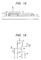
- FIG. 13 is a cross sectional view along the line XIII-XIII of FIG. 11
- FIG. 14 is an explanatory view of a circuit structure.
- the electronic circuit unit in accordance with the present embodiment is used as various high frequency devices, an electronic circuit unit is provided with an alumina substrate 21 on which, for example, an amplifier circuit shown in FIG. 14 is mounted.
- the amplifier circuit has circuit component elements such as capacitors C8 to C10, resistors R4 to R6, an inductance element L4, and a transistor Tr3 and a wiring pattern P2 used to connect these elements.
- the capacitors C8 to C10, resistors R4 to R6, inductance element L4, and wiring pattern P2 are formed by means of thin film process such as spattering or CVD, and the transistor Tr3 is mounted on the alumina substrate 21 by fixing a bare chip by means of wire-bonding.
- FIG. 14 shows only an exemplary circuit structure, and the present invention is applicable to an electronic circuit unit having a structure other than the above-mentioned structure.
- a bottom electrode 22, a dielectric film 23, and a top electrode 24 are laminated one on another on the surface of the alumina substrate 21 to thereby form three thin film capacitors corresponding to the capacitors C8 to C10, and the bottom electrodes 22 and the top electrodes 24 of the capacitors C8 to C10 are connected to the wiring pattern P2.
- the bottom electrodes 22, top electrodes 24, and wiring pattern P2, among these component elements, are formed of Ti/Cu conductive film by forming SiO 2 by means of thin film forming technique, and the dielectric film 23 is formed of dielectric film formed by means of thin film forming technique.
- Resistor films formed of TaSiO 2 corresponding to the resistors R4 to R6 and conductive film formed of Ti/Cu corresponding to the inductance element L4 are formed on the surface of the alumina substrate 21 by means of thin film forming technique, and both ends of these resistor films and conductive film are connected to the wiring pattern P2. Furthermore, a part of the wiring pattern P2 is served as the connection land 25, and the bare chip 26 of the transistor Tr3 is mounted on the connection land 25.
- the top electrode 24 of the thin film capacitor corresponding to the capacitor C9 is served also as a part of the connection land 25, and the bottom side collector electrode 26a of the bare chip 26 is connected to the connection land 25 by use of conductive adhesive 27.
- the capacitor C9 is formed just under the mounting space of the bare chip 26 by means of thin film forming technique, the bare chip 26 and the capacitor C9 are overlapped one on the other.
- the residual capacitors C8 and C10 are served as the ground capacitors, the base electrode 26b and the emitter electrode 26c on the top side of the bare chip 26 are connected to the top electrodes 24 of the respective capacitors C8 and C10 through the wire 28.
- the bare chip 26 is connected to the top electrodes 24 of both ground capacitors C8 and C10 that are served as the bonding pad by means of wire bonding.
- the capacitor C9 is formed just under the space where the bare chip 26 of the transistor Tr3 is mounted by means of thin film forming technique and the top electrode 24 of the capacitor C9 is served also as a part of the connection land 25 of the bare chip 26, the areal efficiency is improved by the area corresponding to overlapped area of the bare chip 26 and the capacitor C9, and the lead inductance component between the bare chip 26 and the capacitor C9 is reduced to result in prevention of the high frequency characteristic deterioration.
- the bare chip 26 is wire-bonded by use of the top electrodes 24 of the ground capacitors C8 and C10 as the bonding pad, the areal efficiency is more improved by the area corresponding to the area of the bonding pad. Both areal efficiency improvements of the bonding pad and the capacitor C9 bring about miniaturization of the electronic circuit unit, and the reduction of the lead inductance component between the bare chip 26 and the capacitors C8 and C10 brings about prevention of high frequency characteristic deterioration.
- the present invention is applied as described in the above-mentioned embodiment and exhibits the effect described hereunder.
- Circuit elements including capacitors, resistors, and inductance elements and conducting patterns connected to these circuit elements are formed on an alumina substrate by means of thin film forming technique, a semiconductor bare chip is fixed to the conducting pattern by means of wire bonding, and the area of the connection land on which the semiconductor bare chip is mounted is made smaller than the bottom surface area of the semiconductor bare chip.
- the electronic circuit unit can be miniaturized.
- the thin film capacitor is formed just under the mounting space of the semiconductor bare chip, the top electrode of the thin film capacitor is served also as a part of the connection land of the semiconductor bare chip, and the top electrode of the thin film capacitor is used as the bonding pad for wiring bonding the semiconductor bare chip.
- the improved areal efficiency of the substrate brings about the miniaturization of the electronic circuit unit but also the reduction of the lead inductance between the thin film capacitors and the semiconductor bare chip brings about prevention of the high frequency characteristic deterioration.
Landscapes
- Engineering & Computer Science (AREA)
- Microelectronics & Electronic Packaging (AREA)
- Manufacturing & Machinery (AREA)
- Semiconductor Integrated Circuits (AREA)
- Structures For Mounting Electric Components On Printed Circuit Boards (AREA)
- Parts Printed On Printed Circuit Boards (AREA)
Abstract
Description
Claims (7)
- An electronic circuit unit comprising a conducting pattern formed on an alumina substrate by means of thin film forming technique, circuit elements including capacitors, resistors, and inductance elements formed on the alumina substrate by means of thin film forming technique so as to be connected to the conducting pattern, and a semiconductor bare chip fixed to the conducting pattern by means of wire bonding, wherein the area of the connection land on which the semiconductor bare chip is mounted is smaller than the bottom surface area of the semiconductor bare chip.
- The electronic circuit unit according to claim 1, wherein at least two sides of the rectangular semiconductor bare chip are located apart from the contour of the connection land.
- The electronic circuit unit according to claim 1, wherein an opening is formed in the connection land.
- The electronic circuit unit according to claim 2, wherein an opening is formed in the connection land.
- An electronic circuit unit having the structure in which a capacitor is formed by laminating a bottom electrode and a top electrode with interposition of a dielectric material on a substrate, and a semiconductor bare chip is mounted so as to be located on the capacitor on the substrate, wherein the top electrode of the capacitor is served as a part of a connection land connected to the bottom side electrode of the semiconductor bare chip.
- An electronic circuit unit having the structure in which a capacitor is formed by laminating a bottom electrode and a top electrode with interposition of a dielectric material on a substrate, and a semiconductor bare chip is mounted on the substrate, wherein the top electrode of the capacitor is connected to the top side electrode of the semiconductor bare chip by means of wire bonding.
- The electronic circuit unit according to claim 5, wherein another capacitor is formed by laminating a bottom electrode and a top electrode with interposition of dielectric material on a substrate, wherein the top electrode of the capacitor is connected to the top side electrode of the semiconductor bare chip by means of wire bonding.
Applications Claiming Priority (4)
| Application Number | Priority Date | Filing Date | Title |
|---|---|---|---|
| JP2000160278A JP3244682B2 (en) | 2000-05-30 | 2000-05-30 | Electronic circuit unit |
| JP2000160278 | 2000-05-30 | ||
| JP2000294671 | 2000-09-27 | ||
| JP2000294671A JP2002110891A (en) | 2000-09-27 | 2000-09-27 | Electronic circuit unit |
Publications (2)
| Publication Number | Publication Date |
|---|---|
| EP1160867A2 true EP1160867A2 (en) | 2001-12-05 |
| EP1160867A3 EP1160867A3 (en) | 2004-05-12 |
Family
ID=26592910
Family Applications (1)
| Application Number | Title | Priority Date | Filing Date |
|---|---|---|---|
| EP01304504A Withdrawn EP1160867A3 (en) | 2000-05-30 | 2001-05-23 | Electronic circuit unit that is suitable for miniaturization and excellent in high frequency charateristic |
Country Status (5)
| Country | Link |
|---|---|
| US (1) | US6603667B2 (en) |
| EP (1) | EP1160867A3 (en) |
| KR (1) | KR100434839B1 (en) |
| CN (1) | CN1197442C (en) |
| TW (1) | TW502492B (en) |
Cited By (1)
| Publication number | Priority date | Publication date | Assignee | Title |
|---|---|---|---|---|
| WO2003107420A1 (en) * | 2002-06-18 | 2003-12-24 | Koninklijke Philips Electronics N.V. | High-frequency integrated transistor module |
Families Citing this family (8)
| Publication number | Priority date | Publication date | Assignee | Title |
|---|---|---|---|---|
| TW517447B (en) * | 2000-05-30 | 2003-01-11 | Alps Electric Co Ltd | Semiconductor electronic circuit unit |
| TW483233B (en) * | 2000-05-30 | 2002-04-11 | Alps Electric Co Ltd | Electronic circuit unit |
| US7948069B2 (en) * | 2004-01-28 | 2011-05-24 | International Rectifier Corporation | Surface mountable hermetically sealed package |
| JP2005294376A (en) * | 2004-03-31 | 2005-10-20 | Toshiba Corp | Magnetic recording element and magnetic memory |
| JP2011238016A (en) * | 2010-05-10 | 2011-11-24 | Sony Corp | Non-contact communication medium, antenna pattern arrangement medium, communication device and antenna adjustment method |
| CN102332414A (en) * | 2011-09-01 | 2012-01-25 | 安徽四创电子股份有限公司 | Method and technology for miniaturizing film amplitude limiting LNA (low noise amplifier) |
| KR102211934B1 (en) * | 2014-03-06 | 2021-02-04 | 삼성전자주식회사 | Semiconductor package |
| US20240057258A1 (en) * | 2021-01-19 | 2024-02-15 | Tdk Corporation | Circuit board |
Family Cites Families (17)
| Publication number | Priority date | Publication date | Assignee | Title |
|---|---|---|---|---|
| US5272590A (en) * | 1990-02-12 | 1993-12-21 | Hernandez Jorge M | Integrated circuit package having an internal cavity for incorporating decoupling capacitor |
| JP2901091B2 (en) * | 1990-09-27 | 1999-06-02 | 株式会社日立製作所 | Semiconductor device |
| JPH0653406A (en) | 1992-07-28 | 1994-02-25 | Matsushita Electric Ind Co Ltd | Formation of thin film circuit |
| JP3461204B2 (en) * | 1993-09-14 | 2003-10-27 | 株式会社東芝 | Multi-chip module |
| JP3047735B2 (en) * | 1994-05-16 | 2000-06-05 | 住友電気工業株式会社 | Optical receiving module and method of manufacturing the same |
| US6020219A (en) * | 1994-06-16 | 2000-02-01 | Lucent Technologies Inc. | Method of packaging fragile devices with a gel medium confined by a rim member |
| DE69524855T2 (en) * | 1994-08-25 | 2002-08-14 | National Semiconductor Corp., Sunnyvale | COMPONENT STACK IN MULTI-CHIP SEMICONDUCTOR PACKS |
| JP3421179B2 (en) * | 1995-09-28 | 2003-06-30 | 株式会社日立国際電気 | Element composite mounted circuit board |
| JPH09283884A (en) * | 1996-04-17 | 1997-10-31 | Kyocera Corp | Circuit board with capacitive element |
| US5825628A (en) * | 1996-10-03 | 1998-10-20 | International Business Machines Corporation | Electronic package with enhanced pad design |
| US5804880A (en) * | 1996-11-04 | 1998-09-08 | National Semiconductor Corporation | Solder isolating lead frame |
| JPH10215119A (en) * | 1997-01-29 | 1998-08-11 | Tdk Corp | Voltage controlled oscillator |
| US6038133A (en) * | 1997-11-25 | 2000-03-14 | Matsushita Electric Industrial Co., Ltd. | Circuit component built-in module and method for producing the same |
| JP3013831B2 (en) * | 1998-01-26 | 2000-02-28 | 日本電気株式会社 | MMIC package |
| US6356455B1 (en) * | 1999-09-23 | 2002-03-12 | Morton International, Inc. | Thin integral resistor/capacitor/inductor package, method of manufacture |
| US6404649B1 (en) * | 2000-03-03 | 2002-06-11 | Advanced Micro Devices, Inc. | Printed circuit board assembly with improved bypass decoupling for BGA packages |
| US6320757B1 (en) * | 2000-07-12 | 2001-11-20 | Advanced Semiconductor Engineering, Inc. | Electronic package |
-
2001
- 2001-05-02 TW TW090110519A patent/TW502492B/en not_active IP Right Cessation
- 2001-05-23 EP EP01304504A patent/EP1160867A3/en not_active Withdrawn
- 2001-05-24 CN CNB011182342A patent/CN1197442C/en not_active Expired - Fee Related
- 2001-05-29 KR KR10-2001-0029763A patent/KR100434839B1/en not_active Expired - Fee Related
- 2001-05-29 US US09/870,416 patent/US6603667B2/en not_active Expired - Fee Related
Cited By (1)
| Publication number | Priority date | Publication date | Assignee | Title |
|---|---|---|---|---|
| WO2003107420A1 (en) * | 2002-06-18 | 2003-12-24 | Koninklijke Philips Electronics N.V. | High-frequency integrated transistor module |
Also Published As
| Publication number | Publication date |
|---|---|
| US20020011352A1 (en) | 2002-01-31 |
| TW502492B (en) | 2002-09-11 |
| KR100434839B1 (en) | 2004-06-07 |
| US6603667B2 (en) | 2003-08-05 |
| KR20010109152A (en) | 2001-12-08 |
| CN1334695A (en) | 2002-02-06 |
| EP1160867A3 (en) | 2004-05-12 |
| CN1197442C (en) | 2005-04-13 |
Similar Documents
| Publication | Publication Date | Title |
|---|---|---|
| US6714420B2 (en) | Electronic circuit unit that is suitable for miniaturization and suitable for simple output adjustment | |
| US6603667B2 (en) | Electronic circuit unit that is suitable for miniaturization and excellent in high frequency characteristic | |
| EP1161124B1 (en) | Surface-mounting type electronic circuit unit suitable for miniaturization | |
| JP3940026B2 (en) | Manufacturing method of electronic circuit unit | |
| US6700177B2 (en) | Compact, surface-mounting-type, electronic-circuit unit | |
| EP1160868B1 (en) | Electronic circuit unit suitable for miniaturization | |
| JP3244677B2 (en) | Electronic circuit unit | |
| JP3246908B2 (en) | Electronic circuit unit | |
| JP3244678B2 (en) | Electronic circuit unit | |
| JP3244682B2 (en) | Electronic circuit unit | |
| JP3244679B2 (en) | Electronic circuit unit | |
| JP3244680B2 (en) | Electronic circuit unit | |
| JP3246907B2 (en) | Electronic circuit unit | |
| JP3244681B2 (en) | Electronic circuit unit | |
| JP2001339243A (en) | Electronic circuit unit | |
| JP2001345643A (en) | Voltage controlled oscillator |
Legal Events
| Date | Code | Title | Description |
|---|---|---|---|
| PUAI | Public reference made under article 153(3) epc to a published international application that has entered the european phase |
Free format text: ORIGINAL CODE: 0009012 |
|
| AK | Designated contracting states |
Kind code of ref document: A2 Designated state(s): AT BE CH CY DE DK ES FI FR GB GR IE IT LI LU MC NL PT SE TR |
|
| AX | Request for extension of the european patent |
Free format text: AL;LT;LV;MK;RO;SI |
|
| PUAL | Search report despatched |
Free format text: ORIGINAL CODE: 0009013 |
|
| RIC1 | Information provided on ipc code assigned before grant |
Ipc: 7H 01L 23/66 B Ipc: 7H 05K 3/40 B Ipc: 7H 05K 5/00 B Ipc: 7H 01L 25/16 A |
|
| AK | Designated contracting states |
Kind code of ref document: A3 Designated state(s): AT BE CH CY DE DK ES FI FR GB GR IE IT LI LU MC NL PT SE TR |
|
| AX | Request for extension of the european patent |
Extension state: AL LT LV MK RO SI |
|
| 17P | Request for examination filed |
Effective date: 20040607 |
|
| AKX | Designation fees paid |
Designated state(s): DE FI FR GB |
|
| 17Q | First examination report despatched |
Effective date: 20060912 |
|
| STAA | Information on the status of an ep patent application or granted ep patent |
Free format text: STATUS: THE APPLICATION IS DEEMED TO BE WITHDRAWN |
|
| 18D | Application deemed to be withdrawn |
Effective date: 20081202 |