EP1160794A1 - Circuit structure for programming data in reference cells of a multibit non-volatile memory device - Google Patents
Circuit structure for programming data in reference cells of a multibit non-volatile memory device Download PDFInfo
- Publication number
- EP1160794A1 EP1160794A1 EP00830392A EP00830392A EP1160794A1 EP 1160794 A1 EP1160794 A1 EP 1160794A1 EP 00830392 A EP00830392 A EP 00830392A EP 00830392 A EP00830392 A EP 00830392A EP 1160794 A1 EP1160794 A1 EP 1160794A1
- Authority
- EP
- European Patent Office
- Prior art keywords
- matrix
- circuit structure
- cells
- sub
- cell
- Prior art date
- Legal status (The legal status is an assumption and is not a legal conclusion. Google has not performed a legal analysis and makes no representation as to the accuracy of the status listed.)
- Granted
Links
- 230000015654 memory Effects 0.000 claims abstract description 57
- 239000011159 matrix material Substances 0.000 claims abstract description 46
- 238000000034 method Methods 0.000 description 10
- 239000004065 semiconductor Substances 0.000 description 3
- 238000010276 construction Methods 0.000 description 2
- 239000000758 substrate Substances 0.000 description 2
- 238000012360 testing method Methods 0.000 description 2
- 230000000052 comparative effect Effects 0.000 description 1
- 238000001514 detection method Methods 0.000 description 1
- 238000011161 development Methods 0.000 description 1
- 230000018109 developmental process Effects 0.000 description 1
- 238000010586 diagram Methods 0.000 description 1
- 230000009977 dual effect Effects 0.000 description 1
- 230000005669 field effect Effects 0.000 description 1
- 238000004519 manufacturing process Methods 0.000 description 1
- 238000012986 modification Methods 0.000 description 1
- 230000004048 modification Effects 0.000 description 1
- 238000012552 review Methods 0.000 description 1
Images

Classifications
-
- G—PHYSICS
- G11—INFORMATION STORAGE
- G11C—STATIC STORES
- G11C7/00—Arrangements for writing information into, or reading information out from, a digital store
- G11C7/10—Input/output [I/O] data interface arrangements, e.g. I/O data control circuits, I/O data buffers
- G11C7/1072—Input/output [I/O] data interface arrangements, e.g. I/O data control circuits, I/O data buffers for memories with random access ports synchronised on clock signal pulse trains, e.g. synchronous memories, self timed memories
-
- G—PHYSICS
- G11—INFORMATION STORAGE
- G11C—STATIC STORES
- G11C11/00—Digital stores characterised by the use of particular electric or magnetic storage elements; Storage elements therefor
- G11C11/56—Digital stores characterised by the use of particular electric or magnetic storage elements; Storage elements therefor using storage elements with more than two stable states represented by steps, e.g. of voltage, current, phase, frequency
- G11C11/5621—Digital stores characterised by the use of particular electric or magnetic storage elements; Storage elements therefor using storage elements with more than two stable states represented by steps, e.g. of voltage, current, phase, frequency using charge storage in a floating gate
-
- G—PHYSICS
- G11—INFORMATION STORAGE
- G11C—STATIC STORES
- G11C11/00—Digital stores characterised by the use of particular electric or magnetic storage elements; Storage elements therefor
- G11C11/56—Digital stores characterised by the use of particular electric or magnetic storage elements; Storage elements therefor using storage elements with more than two stable states represented by steps, e.g. of voltage, current, phase, frequency
- G11C11/5621—Digital stores characterised by the use of particular electric or magnetic storage elements; Storage elements therefor using storage elements with more than two stable states represented by steps, e.g. of voltage, current, phase, frequency using charge storage in a floating gate
- G11C11/5628—Programming or writing circuits; Data input circuits
-
- G—PHYSICS
- G11—INFORMATION STORAGE
- G11C—STATIC STORES
- G11C11/00—Digital stores characterised by the use of particular electric or magnetic storage elements; Storage elements therefor
- G11C11/56—Digital stores characterised by the use of particular electric or magnetic storage elements; Storage elements therefor using storage elements with more than two stable states represented by steps, e.g. of voltage, current, phase, frequency
- G11C11/5621—Digital stores characterised by the use of particular electric or magnetic storage elements; Storage elements therefor using storage elements with more than two stable states represented by steps, e.g. of voltage, current, phase, frequency using charge storage in a floating gate
- G11C11/5628—Programming or writing circuits; Data input circuits
- G11C11/5635—Erasing circuits
-
- G—PHYSICS
- G11—INFORMATION STORAGE
- G11C—STATIC STORES
- G11C11/00—Digital stores characterised by the use of particular electric or magnetic storage elements; Storage elements therefor
- G11C11/56—Digital stores characterised by the use of particular electric or magnetic storage elements; Storage elements therefor using storage elements with more than two stable states represented by steps, e.g. of voltage, current, phase, frequency
- G11C11/5621—Digital stores characterised by the use of particular electric or magnetic storage elements; Storage elements therefor using storage elements with more than two stable states represented by steps, e.g. of voltage, current, phase, frequency using charge storage in a floating gate
- G11C11/5642—Sensing or reading circuits; Data output circuits
-
- G—PHYSICS
- G11—INFORMATION STORAGE
- G11C—STATIC STORES
- G11C16/00—Erasable programmable read-only memories
- G11C16/02—Erasable programmable read-only memories electrically programmable
- G11C16/06—Auxiliary circuits, e.g. for writing into memory
- G11C16/26—Sensing or reading circuits; Data output circuits
- G11C16/28—Sensing or reading circuits; Data output circuits using differential sensing or reference cells, e.g. dummy cells
-
- G—PHYSICS
- G11—INFORMATION STORAGE
- G11C—STATIC STORES
- G11C2211/00—Indexing scheme relating to digital stores characterized by the use of particular electric or magnetic storage elements; Storage elements therefor
- G11C2211/56—Indexing scheme relating to G11C11/56 and sub-groups for features not covered by these groups
- G11C2211/563—Multilevel memory reading aspects
- G11C2211/5634—Reference cells
Definitions
- the invention broadly relates to an electronic multi-level non-volatile memory device which is monolithically integrated in a semiconductor and incorporates a circuit structure for programming data contained in the memory.
- the invention relates to a circuit structure for writing reference cells into a multi-level non-volatile memory, and the following description is made with reference to this field of application for convenience of explanation.
- Electronic memory devices usually comprise at least one matrix of memory cells laid into rows and columns of the matrix. Logic information can be written or read into/from each cell by suitably biasing the corresponding row or column.
- a typical memory cell comprises a field-effect transistor having a control gate terminal, a floating gate region, a source terminal, and a drain terminal.
- a range of electric potentials separates the two possible logic states of a two-level memory cell -- e.g. a logic "0" to indicate a programmed cell, and a logic "1" to indicate an erased cell.
- the memory cell In operation, for the purpose of discriminating the informational contents of a two-level non-volatile memory cell, the memory cell is compared with a structurally identical reference cell which contains a known logic value.
- the operation for selecting a cell in order to read its informational contents consists of applying a suitable bias voltage to the control gate terminal of the memory cell. If the cell has previously been programmed, then an electric charge is trapped within its floating gate region, and the threshold voltage of the cell is such that makes the drain current conduction lower than the reference cell.
- a method most frequently used for reading from a flash type of memory cell consists of comparing the current drawn by the cell to be read and the current drawn by the reference cell.
- a simple comparator known as sense amplifier, is used to perform the comparison and outputs a corresponding result.
- references are needed to discriminate a cell having an n-bit storage capacity; such references may be voltage- or current-oriented, depending on the reading method applied.
- a prior method of determining the state of an n-level memory cell is described in the US Patent No. 5,774,395, wherein the reference cell is electrically erased in order to determine the threshold voltage of the reference cell with high accuracy within a wide range of voltages, e.g. of -5 to 15 Volts.
- selected elements of the multi-level reference cell are electrically erased and re-programmed to allow a detection and a fine tuning of the multiple logic states present in a memory cell, i.e. disallow overlap of cell states.
- the reference cells of a multi-level memory require an additional program circuitry for writing into the reference cells the intermediate logic levels to compare with the programmed or programmable ones in the memory cell matrix.
- the underlying technical problem of this invention is to provide a circuit structure whereby reference cells, preferably but not exclusively of the multi-level type, can be simply and accurately programmed with only a minor impact on the circuit area of the memory device and the programming speed of such reference cells.
- the resolution idea at the basis of the present invention is that of providing, for each matrix block included in a specific read sector, a corresponding external array which contains all the reference cells needed for comparison with the selected matrix cells.
- the reference cells contained in said array are accessed directly using a conventional DMA (Direct Memory Access) technique.
- DMA Direct Memory Access
- a circuit structure for a non-volatile memory device incorporating a matrix of memory cells is generally and schematically shown at 1.
- the memory cells themselves are omitted because conventional.
- This memory device is monolithically integrated on a semiconductor and is electrically programmable/erasable, it being of the EEPROM or the flash type, for example. Furthermore, this memory device can be of the single or the dual supply type.
- the memory matrix is organized into rows or word lines and columns or bit lines.
- Each cell comprises essentially a floating-gate transistor having drain and source regions formed on a semiconductor substrate and separated by a channel region.
- the floating gate is formed on top of the substrate and is isolated therefrom by a thin gate oxide layer.
- a control gate is capacitively coupled to the floating gate through a dielectric layer. The control gate is the control terminal of the transistor, while the drain and source terminals are conduction terminals.
- the matrix of memory cells is preferably divided into a plurality of electrically programmable sectors 2, which can also be programmed by single bytes.
- a number of sectors 2 designated as BLOCK1,...BLOCKi,..., BLOCK7.
- memory cells belonging to the same word line share the electric line which drives the respective control gates, whereas memory cells belonging to the same bit line share the drain terminals.
- the source terminals of the memory cells are all connected to a ground reference.
- the state of the latter can be altered by changing the charge amount present in the floating gate.
- the operation of storing charge into the floating gate is called "programming" and consists of biasing the control gate and the drain terminal to a predetermined voltage value which lies above the potential at the source terminal.
- a flash memory can be programmed either by the sector (page mode) or the byte (byte mode). In the page mode, all the cells of the same matrix row are simultaneously addressed. In the byte mode, a single byte of the plural bytes available is addressed in the same row.
- a voltage approximately equal to the program voltage to the source terminal is applied a voltage approximately equal to the program voltage, while the drain terminal is held floating and the control gate is either connected to ground or to a negative voltage reference. Similar as with programming, a cell can be deleted by single or multiple sectors.
- a memory cell For reading, the current draw of a memory cell is simply compared with that of a reference cell, the latter usually being a virgin cell with the same structure as the matrix cell.
- the reference cells 3 which are compared with the matrix cells during a read phase are contained in a sub-matrix 4 which is structurally independent of the memory matrix.
- the sub-matrix 4 of reference cells 3 is similar in construction to the memory cell matrix, meaning that reference cells 3 belonging to the same word line also share the electric line used for driving their respective control gates, whereas reference cells 3 belonging to the same bit line share the drain terminals in common.
- the reference cells 3 should be regarded as being external of the memory cell matrix and associated with respective additional word lines which are always selected.
- Figure 1 schematically shows a plurality of matrix sectors 2, each having a corresponding sub-matrix 4 of reference cells 3 associated therewith.
- sub-matrix 4 of reference cells 3 is duplicated for each read sector BLOCK0,..., BLOCK7.
- Each sector 2 can comprise two or more outputs, depending on the number of bits stored in the elementary memory cell. These outputs are obviously produced, by a read amplifying block or sense amplifier 5 associated with each sector 2 of the cell matrix.
- conduction paths 6 linking the sub-matrix 4 of reference cells 3 to the sense amplifiers 5 which allow the memory cells to be read.
- the conduction paths 6 comprise bit lines of the sub-matrix 4 of reference cells 3 which extend towards the sense amplifiers 5 through a corresponding series of switches 7, the latter being parallel driven from the output of a logic circuit 8 by means of a signal REFSEL.
- bit lines branch off to a second series of normally open switches 9 which are individually selected and operated by respective control signals REF(i) emitted from the logic circuit 8.
- the second series of switches 9 allows the bit lines of the sub-matrix 4 of reference cells 3 to be connected to a single I/O terminal 10 through a single addressing line 11 over which an addressing signal is transmitted in the DMA mode, as explained hereinafter.
- the logic circuit 8 is input of a synchronization signal REFPROG acting on each read block and being shared by each of the logic circuits 8 incorporated in each block BLOCKi.
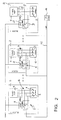
- FIG. 2 Schematically shown in Figure 2 is the internal construction of the logic circuit 8.
- the example of Figure 2 relates to a multi-level memory having an elementary memory cell which is capable to store two informational bits.
- three identical addresses for all the read blocks BLOCK0,..., BLOCK7 (for the three corresponding reference cells), plus another address for selecting the individual block BLOCKi, are all the addresses required.
- the REFSEL signal is basically derived from the logic reversal of the REFPROG signal, e.g. by using an inverter 12.
- the logic circuit 8 further comprises a plurality of logic gates P1, P2, P3,..., Pn, with n being the number of bit lines of the reference cells to be addressed.
- the logic gates may be of the AND type with three inputs. It should be understood that other types of logic gates or a different logic network could be used instead.
- the REFPROG signal is applied to a first input of each of said logic gates P1, P2, P3,..., and an enable signal ADD BLOCK(i) is applied to a second input of each of said logic gates.
- each logic gate P1,P2,P3 receives a respective addressing signal ADD ⁇ 1>, ADD ⁇ 2>, ADD ⁇ 3> from an addressing pin, not shown because conventional.
- each logic gate represents a respective reference signal REF(i) issued from the logic circuit 8 to drive the second series of switches 9.
- the reference cells 3 contained in the sub-matrix 4, external of the memory cell matrix, are directly accessible by the DMA (Direct Memory Address) technique. It should be noted that, contrary to standard two-level EPROMs, the reference cells 3 are not placed on reference bit lines similar to those of the memory matrix. This peculiarity is due to the DMA programming since, if all the cells connected to the reference bit lines were to be DMA programmed, program time would be inordinately long.
- DMA Direct Memory Address
- the presence of the only I/O terminal 10 is particularly advantageous to shorten the program time, since multiple I/O terminals would be hardly driven by testing equipment.
- each read block BLOCKi is multiplexed outward, in this invention, through a single DMA mode addressing line.
- the whole writing operation is controlled by the REFPROG synchronization signal ,which acts on each read block BLOCKi.
- the path of the DMA addressing line 11, leading to each of the selected reference cells, is activated through the series of switches 9 as suitably driven from the logic circuit 8.
- the reference cells are always read using the DMA technique, so that their values can be checked.
- the DMA method has a major advantage in that the addressed reference cell can be programmed by a set of voltages suitably calibrated by the testing equipment. Also, the current being delivered therefrom can be measured by a further accurate check of its written state.
- the circuit structure of this invention does solve the technical problem and offers a lot of advantages, foremost among which is that it provides a simple and accurately controlled writing process of the reference cells of a multi-level memory. And this is obtained with minimized area occupation and circuit complexity.
- the programming time of the reference cells is kept substantially the same for each matrix sector.
Landscapes
- Engineering & Computer Science (AREA)
- Computer Hardware Design (AREA)
- Read Only Memory (AREA)
Abstract
Description
- The invention broadly relates to an electronic multi-level non-volatile memory device which is monolithically integrated in a semiconductor and incorporates a circuit structure for programming data contained in the memory.
- In particular, the invention relates to a circuit structure for writing reference cells into a multi-level non-volatile memory, and the following description is made with reference to this field of application for convenience of explanation.
- As it is well known in this specific technical field, recent developments in the manufacture of non-volatile memories, specifically memories of the EPROM, EEPROM and FLASH types, point toward an increase of their storage capacity by the adoption of multi-level architectures, that is, memory matrices whose cells can store multiple logic states.
- A preliminary comparative review of the circuit structures with conventional two-level memories may help, however, to make the aspects of this invention more clearly understood.
- Electronic memory devices usually comprise at least one matrix of memory cells laid into rows and columns of the matrix. Logic information can be written or read into/from each cell by suitably biasing the corresponding row or column.
- A typical memory cell comprises a field-effect transistor having a control gate terminal, a floating gate region, a source terminal, and a drain terminal. A range of electric potentials separates the two possible logic states of a two-level memory cell -- e.g. a logic "0" to indicate a programmed cell, and a logic "1" to indicate an erased cell.
- In operation, for the purpose of discriminating the informational contents of a two-level non-volatile memory cell, the memory cell is compared with a structurally identical reference cell which contains a known logic value.
- The operation for selecting a cell in order to read its informational contents consists of applying a suitable bias voltage to the control gate terminal of the memory cell. If the cell has previously been programmed, then an electric charge is trapped within its floating gate region, and the threshold voltage of the cell is such that makes the drain current conduction lower than the reference cell.
- On the other hand, if the cell has been erased, no electric charge is trapped within its floating gate region, and the conduction state of the cell can be identified using an unbalanced-load technique of comparison with the reference cell.
- Thus, a method most frequently used for reading from a flash type of memory cell consists of comparing the current drawn by the cell to be read and the current drawn by the reference cell. A simple comparator, known as sense amplifier, is used to perform the comparison and outputs a corresponding result.
- In the instance of a multi-level memory device, no less than 2n-1 references are needed to discriminate a cell having an n-bit storage capacity; such references may be voltage- or current-oriented, depending on the reading method applied.
- As an example, a prior method of determining the state of an n-level memory cell is described in the US Patent No. 5,774,395, wherein the reference cell is electrically erased in order to determine the threshold voltage of the reference cell with high accuracy within a wide range of voltages, e.g. of -5 to 15 Volts. Briefly, selected elements of the multi-level reference cell are electrically erased and re-programmed to allow a detection and a fine tuning of the multiple logic states present in a memory cell, i.e. disallow overlap of cell states.
- Thus, unlike a two-level memory, the reference cells of a multi-level memory require an additional program circuitry for writing into the reference cells the intermediate logic levels to compare with the programmed or programmable ones in the memory cell matrix.
- The prior art conventionally used in two-level non-volatile memories provides for allocation of the reference cells and of memory cells to the same matrix. However, this solution is not easily extended to multi-level memories because this would require a circuit area increase with the number of bits, and because the reference cells of a multi-level memory must be programmed.
- These difficulties are emphasized by the use of different reference cells for reading and programming. In fact, a reference line including the same number of reference cells as the matrix cells could affect the reference cell read and/or program time quite significantly.
- The underlying technical problem of this invention is to provide a circuit structure whereby reference cells, preferably but not exclusively of the multi-level type, can be simply and accurately programmed with only a minor impact on the circuit area of the memory device and the programming speed of such reference cells.
- The resolution idea at the basis of the present invention is that of providing, for each matrix block included in a specific read sector, a corresponding external array which contains all the reference cells needed for comparison with the selected matrix cells. The reference cells contained in said array are accessed directly using a conventional DMA (Direct Memory Access) technique.
- Based on this concept, the technical problem is solved by a circuit structure as previously indicated and defined in the appended claims.
- The features and advantages of a circuit structure according to the invention will be apparent from the following description of an embodiment thereof, given by way of non-limitative example with reference to the accompanying drawings.
-
- Figure 1 schematically shows a circuit structure, formed according to the invention, for an electrically programmable/erasable non-volatile memory device incorporating a matrix of multi-level memory cells.
- Figure 2 shows a schematic view of a particular of the circuit structure according to the invention.
-
- Referring to the drawings, a circuit structure for a non-volatile memory device incorporating a matrix of memory cells, according to this invention, is generally and schematically shown at 1. The memory cells themselves are omitted because conventional.
- This memory device is monolithically integrated on a semiconductor and is electrically programmable/erasable, it being of the EEPROM or the flash type, for example. Furthermore, this memory device can be of the single or the dual supply type.
- The following considerations apply, however, to any other type of EEPROM or flash memories, as well as to EPROMs.
- The memory matrix is organized into rows or word lines and columns or bit lines. Each cell comprises essentially a floating-gate transistor having drain and source regions formed on a semiconductor substrate and separated by a channel region. The floating gate is formed on top of the substrate and is isolated therefrom by a thin gate oxide layer. A control gate is capacitively coupled to the floating gate through a dielectric layer. The control gate is the control terminal of the transistor, while the drain and source terminals are conduction terminals.
- The matrix of memory cells is preferably divided into a plurality of electrically
programmable sectors 2, which can also be programmed by single bytes. For explanation purposes only, in the diagram of Figure 1 is shown how the matrix may be regarded as formed by the whole of a number ofsectors 2 designated as BLOCK1,...BLOCKi,..., BLOCK7. - As it is well known, memory cells belonging to the same word line share the electric line which drives the respective control gates, whereas memory cells belonging to the same bit line share the drain terminals. The source terminals of the memory cells are all connected to a ground reference.
- With suitable voltage values being applied to the terminals of a memory cell, the state of the latter can be altered by changing the charge amount present in the floating gate. The operation of storing charge into the floating gate is called "programming" and consists of biasing the control gate and the drain terminal to a predetermined voltage value which lies above the potential at the source terminal.
- A flash memory can be programmed either by the sector (page mode) or the byte (byte mode). In the page mode, all the cells of the same matrix row are simultaneously addressed. In the byte mode, a single byte of the plural bytes available is addressed in the same row.
- To erase a flash memory cell, to the source terminal is applied a voltage approximately equal to the program voltage, while the drain terminal is held floating and the control gate is either connected to ground or to a negative voltage reference. Similar as with programming, a cell can be deleted by single or multiple sectors.
- For reading, the current draw of a memory cell is simply compared with that of a reference cell, the latter usually being a virgin cell with the same structure as the matrix cell.
- Advantageously in this invention, the
reference cells 3 which are compared with the matrix cells during a read phase are contained in asub-matrix 4 which is structurally independent of the memory matrix. - The
sub-matrix 4 ofreference cells 3 is similar in construction to the memory cell matrix, meaning thatreference cells 3 belonging to the same word line also share the electric line used for driving their respective control gates, whereasreference cells 3 belonging to the same bit line share the drain terminals in common. - However, the
reference cells 3 should be regarded as being external of the memory cell matrix and associated with respective additional word lines which are always selected. - It might occur to the skilled person in the art of adding some redundant reference word lines in order to ensure a quantum of redundancy to the
reference cells 3 in the event of one of these cells being damaged. In fact, a single damagedreference cell 3 would be enough to impair the operability of the whole memory device. - Figure 1 schematically shows a plurality of
matrix sectors 2, each having acorresponding sub-matrix 4 ofreference cells 3 associated therewith. - Thus, the
sub-matrix 4 ofreference cells 3 is duplicated for each read sector BLOCK0,..., BLOCK7. - Each
sector 2 can comprise two or more outputs, depending on the number of bits stored in the elementary memory cell. These outputs are obviously produced, by a read amplifying block orsense amplifier 5 associated with eachsector 2 of the cell matrix. - Also provided are
conduction paths 6 linking thesub-matrix 4 ofreference cells 3 to thesense amplifiers 5 which allow the memory cells to be read. - More particularly, the
conduction paths 6 comprise bit lines of thesub-matrix 4 ofreference cells 3 which extend towards thesense amplifiers 5 through a corresponding series ofswitches 7, the latter being parallel driven from the output of alogic circuit 8 by means of a signal REFSEL. - In addition, these bit lines branch off to a second series of normally open switches 9 which are individually selected and operated by respective control signals REF(i) emitted from the
logic circuit 8. - The second series of switches 9 allows the bit lines of the
sub-matrix 4 ofreference cells 3 to be connected to a single I/O terminal 10 through a single addressingline 11 over which an addressing signal is transmitted in the DMA mode, as explained hereinafter. - The
logic circuit 8 is input of a synchronization signal REFPROG acting on each read block and being shared by each of thelogic circuits 8 incorporated in each block BLOCKi. - Schematically shown in Figure 2 is the internal construction of the
logic circuit 8. In particular, the example of Figure 2 relates to a multi-level memory having an elementary memory cell which is capable to store two informational bits. Thus, to address the three reference cells needed for discriminating the four levels of the memory cells, three identical addresses for all the read blocks BLOCK0,..., BLOCK7 (for the three corresponding reference cells), plus another address for selecting the individual block BLOCKi, are all the addresses required. - Likewise, with a memory device having sixteen outputs, two for each read block BLOCKi, eleven addresses would be required.
- The REFSEL signal is basically derived from the logic reversal of the REFPROG signal, e.g. by using an
inverter 12. - The
logic circuit 8 further comprises a plurality of logic gates P1, P2, P3,..., Pn, with n being the number of bit lines of the reference cells to be addressed. For example, the logic gates may be of the AND type with three inputs. It should be understood that other types of logic gates or a different logic network could be used instead. - The REFPROG signal is applied to a first input of each of said logic gates P1, P2, P3,..., and an enable signal ADD BLOCK(i) is applied to a second input of each of said logic gates.
- The third input of each logic gate P1,P2,P3 receives a respective addressing signal ADD<1>, ADD<2>, ADD<3> from an addressing pin, not shown because conventional.
- The output of each logic gate represents a respective reference signal REF(i) issued from the
logic circuit 8 to drive the second series of switches 9. - The method of operating the circuit structure according to the invention will now be described with reference to a memory device which incorporates multi-level memory cells.
- The
reference cells 3 contained in thesub-matrix 4, external of the memory cell matrix, are directly accessible by the DMA (Direct Memory Address) technique. It should be noted that, contrary to standard two-level EPROMs, thereference cells 3 are not placed on reference bit lines similar to those of the memory matrix. This peculiarity is due to the DMA programming since, if all the cells connected to the reference bit lines were to be DMA programmed, program time would be inordinately long. - Furthermore, the presence of the only I/
O terminal 10 is particularly advantageous to shorten the program time, since multiple I/O terminals would be hardly driven by testing equipment. - Accordingly, each read block BLOCKi is multiplexed outward, in this invention, through a single DMA mode addressing line.
- The whole writing operation is controlled by the REFPROG synchronization signal ,which acts on each read block BLOCKi.
- The path of the
DMA addressing line 11, leading to each of the selected reference cells, is activated through the series of switches 9 as suitably driven from thelogic circuit 8. - The reference cells are always read using the DMA technique, so that their values can be checked.
- The DMA method has a major advantage in that the addressed reference cell can be programmed by a set of voltages suitably calibrated by the testing equipment. Also, the current being delivered therefrom can be measured by a further accurate check of its written state.
- The circuit structure of this invention does solve the technical problem and offers a lot of advantages, foremost among which is that it provides a simple and accurately controlled writing process of the reference cells of a multi-level memory. And this is obtained with minimized area occupation and circuit complexity.
- Furthermore, the programming time of the reference cells is kept substantially the same for each matrix sector.
- It should be understood that changes and modifications, within the scope of the following claims, may be made to the circuit structure of this-invention by a skilled person in the art.
Claims (9)
- A circuit structure (1) for programming data in reference cells (3) of an electrically programmable/erasable integrated non-volatile memory device, comprising a matrix of multi-level memory cells and at least a corresponding reference cell provided for comparison with a respective memory cell during the read phase, characterized in that said reference cell (3) is incorporated to a reference cell sub-matrix (4) which is structurally independent of the memory cell matrix and directly accessed from outside in the DMA mode.
- A circuit structure according to Claim 1, characterized in that a conduction path (6) is established between the sub-matrix (4) and the sense amplifiers (5), which are arranged for reading data from the cell matrix; said path (6) including bit lines of the sub-matrix (4) of reference cells (3), which are extended to said sense amplifiers (5) through a corresponding series of switches (7) driven in parallel by the output from a logic circuit (8).
- A circuit structure according to Claim 2, characterized in that said bit lines of the sub-matrix (4) branch off to a second series of switches (9) which are selected and individually operated by respective control signals REF(i) issued from said logic circuit (8).
- A circuit structure according to Claim 3, characterized in that said second series of switches (9) links the bit lines of the sub.matrix (4) of reference cells (3) to a single terminal (10) through a single address line (11) in the DMA access mode.
- A circuit structure according to Claim 2, characterized in that said logic circuit (8) comprises a network of logic gates (P1,P2,P3,...,Pn), all arranged to receive a synchronization signal (REFPROG) applied to each read block (BLOCKi) of the memory matrix.
- A circuit structure according to Claim 5, characterized in that said synchronization signal (REFPROG) is applied to a first input of each of said logic gates (P1,P2,P3,...,Pn); and in that an enable signal (ADD BLOCK(i)) of the respective read block (BLOCKi) is applied to a second input of each of said logic gates; and in that at least a third input of each logic gate (P1,P2,P3,...,Pn) receives a respective addressing signal (ADD<1>;ADD<2>;ADD<3>,...) from an address pin.
- A circuit structure according to Claim 1, characterized in that a submatrix (4) of reference cells (3) is duplicated for each read sector (BLOCK0,...,BLOCK7) of the memory cell matrix.
- A circuit structure according to Claim 7, characterized in that each read block (BLOCKi) is multiplexed outward through the only addressing line (11) in the DMA mode.
- A circuit structure according to Claim 1, characterized in that said sub-matrix (4) includes additional redundant word lines.
Priority Applications (3)
| Application Number | Priority Date | Filing Date | Title |
|---|---|---|---|
| EP00830392A EP1160794B1 (en) | 2000-05-31 | 2000-05-31 | Circuit structure for programming data in reference cells of a multibit non-volatile memory device |
| DE60039587T DE60039587D1 (en) | 2000-05-31 | 2000-05-31 | Circuit arrangement for programming data in reference cells of a non-volatile multi-bit memory arrangement |
| US09/871,235 US6507517B2 (en) | 2000-05-31 | 2001-05-30 | Circuital structure for programming data in a non-volatile memory device |
Applications Claiming Priority (1)
| Application Number | Priority Date | Filing Date | Title |
|---|---|---|---|
| EP00830392A EP1160794B1 (en) | 2000-05-31 | 2000-05-31 | Circuit structure for programming data in reference cells of a multibit non-volatile memory device |
Publications (2)
| Publication Number | Publication Date |
|---|---|
| EP1160794A1 true EP1160794A1 (en) | 2001-12-05 |
| EP1160794B1 EP1160794B1 (en) | 2008-07-23 |
Family
ID=8175352
Family Applications (1)
| Application Number | Title | Priority Date | Filing Date |
|---|---|---|---|
| EP00830392A Expired - Lifetime EP1160794B1 (en) | 2000-05-31 | 2000-05-31 | Circuit structure for programming data in reference cells of a multibit non-volatile memory device |
Country Status (3)
| Country | Link |
|---|---|
| US (1) | US6507517B2 (en) |
| EP (1) | EP1160794B1 (en) |
| DE (1) | DE60039587D1 (en) |
Families Citing this family (9)
| Publication number | Priority date | Publication date | Assignee | Title |
|---|---|---|---|---|
| EP1473739A1 (en) * | 2003-04-29 | 2004-11-03 | Dialog Semiconductor GmbH | Flash memory with pre-detection for data loss |
| EP1750281B1 (en) * | 2005-07-29 | 2011-07-06 | STMicroelectronics Srl | Nonvolatile memory device with multiple references and corresponding control method |
| US7180795B1 (en) * | 2005-08-05 | 2007-02-20 | Atmel Corporation | Method of sensing an EEPROM reference cell |
| US7817467B2 (en) * | 2007-09-07 | 2010-10-19 | Micron Technology, Inc. | Memory controller self-calibration for removing systemic influence |
| MY187143A (en) | 2010-01-20 | 2021-09-03 | Semiconductor Energy Lab | Semiconductor device |
| KR102189824B1 (en) * | 2014-08-04 | 2020-12-11 | 삼성전자주식회사 | Unit array of memory device, memory device and memory system including the same |
| KR102420735B1 (en) | 2016-08-19 | 2022-07-14 | 가부시키가이샤 한도오따이 에네루기 켄큐쇼 | Power control method for semiconductor devices |
| CN108875926A (en) * | 2017-10-30 | 2018-11-23 | 上海寒武纪信息科技有限公司 | Interaction language translating method and Related product |
| US11990137B2 (en) | 2018-09-13 | 2024-05-21 | Shanghai Cambricon Information Technology Co., Ltd. | Image retouching method and terminal device |
Citations (4)
| Publication number | Priority date | Publication date | Assignee | Title |
|---|---|---|---|---|
| US5444656A (en) * | 1994-06-02 | 1995-08-22 | Intel Corporation | Apparatus for fast internal reference cell trimming |
| EP0753859A1 (en) * | 1995-07-14 | 1997-01-15 | STMicroelectronics S.r.l. | Method for setting the threshold voltage of a reference memory cell |
| EP0798727A1 (en) * | 1996-03-29 | 1997-10-01 | STMicroelectronics S.r.l. | Data reading path management architecture for a memory device, particularly for non-volatile memories |
| US5905673A (en) * | 1995-10-06 | 1999-05-18 | Agate Semiconductor, Inc. | Integrated circuit for storage and retrieval of multiple digital bits per nonvolatile memory cell |
Family Cites Families (10)
| Publication number | Priority date | Publication date | Assignee | Title |
|---|---|---|---|---|
| JP3324129B2 (en) | 1991-12-27 | 2002-09-17 | 株式会社日立製作所 | Semiconductor multilevel memory |
| RU2190260C2 (en) | 1994-06-02 | 2002-09-27 | Интел Корпорейшн | Reading circuit for flash storage with multilevel cells |
| US5629892A (en) | 1995-10-16 | 1997-05-13 | Advanced Micro Devices, Inc. | Flash EEPROM memory with separate reference array |
| EP0805454A1 (en) * | 1996-04-30 | 1997-11-05 | STMicroelectronics S.r.l. | Sensing circuit for reading and verifying the content of a memory cell |
| US5774395A (en) | 1996-11-27 | 1998-06-30 | Advanced Micro Devices, Inc. | Electrically erasable reference cell for accurately determining threshold voltage of a non-volatile memory at a plurality of threshold voltage levels |
| JP3990485B2 (en) * | 1997-12-26 | 2007-10-10 | 株式会社ルネサステクノロジ | Semiconductor nonvolatile memory device |
| JP3237610B2 (en) * | 1998-05-19 | 2001-12-10 | 日本電気株式会社 | Nonvolatile semiconductor memory device |
| EP0978844B1 (en) | 1998-08-07 | 2005-11-02 | STMicroelectronics S.r.l. | Sensing arrangement for a multilevel semiconductor memory device |
| US5936906A (en) | 1998-10-29 | 1999-08-10 | Winbond Electronics Corp. | Multilevel sense device for a flash memory |
| US6317362B1 (en) * | 1999-07-13 | 2001-11-13 | Sanyo Electric Co., Ltd. | Semiconductor memory device |
-
2000
- 2000-05-31 EP EP00830392A patent/EP1160794B1/en not_active Expired - Lifetime
- 2000-05-31 DE DE60039587T patent/DE60039587D1/en not_active Expired - Lifetime
-
2001
- 2001-05-30 US US09/871,235 patent/US6507517B2/en not_active Expired - Lifetime
Patent Citations (4)
| Publication number | Priority date | Publication date | Assignee | Title |
|---|---|---|---|---|
| US5444656A (en) * | 1994-06-02 | 1995-08-22 | Intel Corporation | Apparatus for fast internal reference cell trimming |
| EP0753859A1 (en) * | 1995-07-14 | 1997-01-15 | STMicroelectronics S.r.l. | Method for setting the threshold voltage of a reference memory cell |
| US5905673A (en) * | 1995-10-06 | 1999-05-18 | Agate Semiconductor, Inc. | Integrated circuit for storage and retrieval of multiple digital bits per nonvolatile memory cell |
| EP0798727A1 (en) * | 1996-03-29 | 1997-10-01 | STMicroelectronics S.r.l. | Data reading path management architecture for a memory device, particularly for non-volatile memories |
Also Published As
| Publication number | Publication date |
|---|---|
| DE60039587D1 (en) | 2008-09-04 |
| US6507517B2 (en) | 2003-01-14 |
| US20020015326A1 (en) | 2002-02-07 |
| EP1160794B1 (en) | 2008-07-23 |
Similar Documents
| Publication | Publication Date | Title |
|---|---|---|
| KR101127413B1 (en) | Non-volatile memory and control with improved partial page program capability | |
| US8234440B2 (en) | Nonvolatile semiconductor memory device with advanced multi-page program operation | |
| US6480415B2 (en) | Nonvolatile semiconductor memory device | |
| US7313023B2 (en) | Partition of non-volatile memory array to reduce bit line capacitance | |
| US5270980A (en) | Sector erasable flash EEPROM | |
| US5586075A (en) | Electrically erasable and programmable read-only memory having redundant memory cell row | |
| JP3833970B2 (en) | Nonvolatile semiconductor memory | |
| US6735727B1 (en) | Flash memory device with a novel redundancy selection circuit and method of using the same | |
| KR100536613B1 (en) | Nor type flash memory device being capable of reducing program time and its program method | |
| US6826081B2 (en) | Nonvolatile semiconductor memory device, nonvolatile semiconductor memory device-integrated system, and defective block detecting method | |
| US6661709B2 (en) | Nonvolatile semiconductor memory device | |
| US6891755B2 (en) | Architecture for a flash-EEPROM simultaneously readable in other sectors while erasing and/or programming one or more sectors | |
| US6262914B1 (en) | Flash memory segmentation | |
| US6568510B2 (en) | Flash memory including means of checking memory cell threshold voltages | |
| KR100491912B1 (en) | Nonvolatile semiconductor memory | |
| EP1160794B1 (en) | Circuit structure for programming data in reference cells of a multibit non-volatile memory device | |
| JPH0466080B2 (en) | ||
| US6118695A (en) | Nonvolatile semiconductor memory device | |
| US20100008142A1 (en) | Nonvolatile memory device and method of operating the same | |
| US6842376B2 (en) | Non-volatile semiconductor memory device for selectively re-checking word lines | |
| US6549473B2 (en) | Circuital structure for reading data in a non-volatile memory device | |
| KR19990013057A (en) | Read and write method of flash memory device for selectively storing single bit data and multiple bit data on same chip | |
| EP1011105B1 (en) | One-chip microcomputer | |
| KR100222811B1 (en) | Nonvolatile semiconductor device | |
| JP3197858B2 (en) | Semiconductor memory device |
Legal Events
| Date | Code | Title | Description |
|---|---|---|---|
| PUAI | Public reference made under article 153(3) epc to a published international application that has entered the european phase |
Free format text: ORIGINAL CODE: 0009012 |
|
| AK | Designated contracting states |
Kind code of ref document: A1 Designated state(s): AT BE CH CY DE DK ES FI FR GB GR IE IT LI LU MC NL PT SE Kind code of ref document: A1 Designated state(s): DE FR GB IT |
|
| AX | Request for extension of the european patent |
Free format text: AL;LT;LV;MK;RO;SI |
|
| 17P | Request for examination filed |
Effective date: 20020208 |
|
| AKX | Designation fees paid |
Free format text: DE FR GB IT |
|
| 17Q | First examination report despatched |
Effective date: 20050504 |
|
| 17Q | First examination report despatched |
Effective date: 20050504 |
|
| GRAP | Despatch of communication of intention to grant a patent |
Free format text: ORIGINAL CODE: EPIDOSNIGR1 |
|
| GRAS | Grant fee paid |
Free format text: ORIGINAL CODE: EPIDOSNIGR3 |
|
| GRAA | (expected) grant |
Free format text: ORIGINAL CODE: 0009210 |
|
| AK | Designated contracting states |
Kind code of ref document: B1 Designated state(s): DE FR GB IT |
|
| REG | Reference to a national code |
Ref country code: GB Ref legal event code: FG4D |
|
| REF | Corresponds to: |
Ref document number: 60039587 Country of ref document: DE Date of ref document: 20080904 Kind code of ref document: P |
|
| PLBE | No opposition filed within time limit |
Free format text: ORIGINAL CODE: 0009261 |
|
| STAA | Information on the status of an ep patent application or granted ep patent |
Free format text: STATUS: NO OPPOSITION FILED WITHIN TIME LIMIT |
|
| 26N | No opposition filed |
Effective date: 20090424 |
|
| PG25 | Lapsed in a contracting state [announced via postgrant information from national office to epo] |
Ref country code: IT Free format text: LAPSE BECAUSE OF FAILURE TO SUBMIT A TRANSLATION OF THE DESCRIPTION OR TO PAY THE FEE WITHIN THE PRESCRIBED TIME-LIMIT Effective date: 20080723 |
|
| GBPC | Gb: european patent ceased through non-payment of renewal fee |
Effective date: 20090531 |
|
| REG | Reference to a national code |
Ref country code: FR Ref legal event code: ST Effective date: 20100129 |
|
| PG25 | Lapsed in a contracting state [announced via postgrant information from national office to epo] |
Ref country code: FR Free format text: LAPSE BECAUSE OF NON-PAYMENT OF DUE FEES Effective date: 20090602 |
|
| PG25 | Lapsed in a contracting state [announced via postgrant information from national office to epo] |
Ref country code: GB Free format text: LAPSE BECAUSE OF NON-PAYMENT OF DUE FEES Effective date: 20090531 |
|
| REG | Reference to a national code |
Ref country code: DE Ref legal event code: R082 Ref document number: 60039587 Country of ref document: DE Representative=s name: SAMSON & PARTNER, PATENTANWAELTE, DE |
|
| REG | Reference to a national code |
Ref country code: DE Ref legal event code: R081 Ref document number: 60039587 Country of ref document: DE Owner name: MICRON TECHNOLOGY, INC., US Free format text: FORMER OWNER: STMICROELECTRONICS S.R.L., AGRATE BRIANZA, IT Effective date: 20130515 Ref country code: DE Ref legal event code: R082 Ref document number: 60039587 Country of ref document: DE Representative=s name: SAMSON & PARTNER, PATENTANWAELTE, DE Effective date: 20130515 Ref country code: DE Ref legal event code: R082 Ref document number: 60039587 Country of ref document: DE Representative=s name: SAMSON & PARTNER PATENTANWAELTE MBB, DE Effective date: 20130515 Ref country code: DE Ref legal event code: R081 Ref document number: 60039587 Country of ref document: DE Owner name: MICRON TECHNOLOGY, INC., BOISE, US Free format text: FORMER OWNER: STMICROELECTRONICS S.R.L., AGRATE BRIANZA, MAILAND/MILANO, IT Effective date: 20130515 Ref country code: DE Ref legal event code: R081 Ref document number: 60039587 Country of ref document: DE Owner name: MICRON TECHNOLOGY, INC., BOISE, US Free format text: FORMER OWNER: STMICROELECTRONICS S.R.L., AGRATE BRIANZA, IT Effective date: 20130515 |
|
| PGFP | Annual fee paid to national office [announced via postgrant information from national office to epo] |
Ref country code: DE Payment date: 20150527 Year of fee payment: 16 |
|
| REG | Reference to a national code |
Ref country code: DE Ref legal event code: R119 Ref document number: 60039587 Country of ref document: DE |
|
| PG25 | Lapsed in a contracting state [announced via postgrant information from national office to epo] |
Ref country code: DE Free format text: LAPSE BECAUSE OF NON-PAYMENT OF DUE FEES Effective date: 20161201 |