EP1160793A2 - Memory decoder and method of operation - Google Patents
Memory decoder and method of operation Download PDFInfo
- Publication number
- EP1160793A2 EP1160793A2 EP01304407A EP01304407A EP1160793A2 EP 1160793 A2 EP1160793 A2 EP 1160793A2 EP 01304407 A EP01304407 A EP 01304407A EP 01304407 A EP01304407 A EP 01304407A EP 1160793 A2 EP1160793 A2 EP 1160793A2
- Authority
- EP
- European Patent Office
- Prior art keywords
- row
- memory
- address
- sub
- rows
- Prior art date
- Legal status (The legal status is an assumption and is not a legal conclusion. Google has not performed a legal analysis and makes no representation as to the accuracy of the status listed.)
- Granted
Links
Images


Classifications
-
- G—PHYSICS
- G11—INFORMATION STORAGE
- G11C—STATIC STORES
- G11C8/00—Arrangements for selecting an address in a digital store
Definitions
- the present invention is generally directed to data processors and, more specifically, to a memory circuit capable of storing a current value and previous values of a variable in an address location.
- the present invention also makes the use of certain non-volatile memories transparent to data processors by making them appear functionally equivalent to standard random access memories.
- a number of techniques may be used to debug a conventional microprocessor and/or to debug software executed by a microprocessor.
- One technique involves editing source code to include unique print statements associated with particular program branches in order to determine the paths the program took during execution.
- Another technique involves using a debugger, which causes a program to execute to some break point and then halt. This allows a programmer to modify memory, to analyze certain registers (such as debug registers) that are accessible in the microprocessor, and to change break points, if necessary. Program execution may then be resumed.
- non-volatile memories also called flash memories or electrically erasable programmable memories (EEPROM) offer enhanced functionality to the data processing system.
- these memories often require special access instructions or procedures which are not used by conventional volatile memories. For instance, a flash memory must be erased in sectors instead of single memory locations.
- a conventional random access memory can be read and written one storage location at a time. The flash memory must be erased before any new values can be overwritten at an already used location. This makes the use of flash memory impractical at the system level, because in order to change the contents of one location, an entire sector must be erased and rewritten.
- the memory comprises a memory block comprising R rows of memory cells and a row address decoder capable of decoding the first memory address, wherein the row address decoder during a read operation causes data to be retrieved from a row in which data stored to the first memory address was last written and wherein the row address decoder during a write operation causes data to be stored in a next-sequential row following the last-written row.
- the R rows of memory cells are divided into S sub-blocks of rows, each of the S sub-blocks comprising M rows of memory cells, wherein the first memory address accesses a first one of the S sub-blocks of rows.
- the row address decoder comprises a first decoder capable of decoding the first memory address and generating therefrom a sub-block selection signal capable of accessing the first sub-block.
- the row address decoder comprises a second decoder capable of receiving the sub-block selection signal and generating therefrom a row selection signal capable of accessing one of the next-sequential row and the last-written row in the first sub-block.
- the second decoder is further capable of receiving a read/write signal indicating whether a pending memory access operation is a write operation and, if the pending memory access operation is a write operation, generating the row selection signal to allow data to be written to the next-sequential row.
- the second decoder if the pending memory access operation is a read operation, generates the row selection signal to allow data to be retrieved from the last-written row.
- the memory further comprises a debugging controller coupled to the row address controller and capable of causing the row address controller to sequentially read data from each of the M rows of memory cells in the first sub-block to thereby retrieve the present value and the at least one past value of the variable accessible by the first memory address.
- a debugging controller coupled to the row address controller and capable of causing the row address controller to sequentially read data from each of the M rows of memory cells in the first sub-block to thereby retrieve the present value and the at least one past value of the variable accessible by the first memory address.
- FIGURES 1 through 4 discussed below, and the various embodiments used to describe the principles of the present invention in this patent document are by way of illustration only and should not be construed in any way to limit the scope of the invention. Those skilled in the art will understand that the principles of the present invention may be implemented in any suitably arranged non-volatile memory.
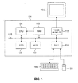
- FIGURE 1 illustrates an exemplary processing system, namely personal computer (PC) 100, that contains a non-volatile memory in accordance with the principles of the present invention.
- Personal computer 100 comprises removable (i.e., floppy) disk drive 102 and hard disk drive 103, monitor 104, keyboard 105, processor (CPU) 106, main memory 107, and a pointing device, such as mouse 108.
- Monitor 104, keyboard 105, and mouse 108 may be replaced by, or combined with, other input/output (I/O) devices.
- Removable disk drive 102 is capable of reading and writing to removable floppy diskettes.
- Hard disk drive 105 provides fast access for storage and retrieval of application programs and data.
- Keyboard 105 and mouse 108 are coupled to PC 100 via input/output (I/O) interface (IF) 110.
- Monitor 104 is coupled to PC 100 via video/audio interface (IF) 112.
- the internal components of PC 100 including floppy disk drive 102, hard disk drive 103, processor 106, main memory 107, I/O interface 110 and video/audio interface 112, are coupled to and communicate across communications bus 115.
- main memory 107 comprises a volatile storage device, such as a dynamic random access memory (RAM).
- Processor 106 may comprise an on-board two level cache system, including a Level 1 (L1) cache and a Level 2 (L2) cache.
- the two level cache is a system in which a small, fast cache (the L1 cache) is connected to a slower, larger cache (the L2 cache).
- the cache system first tests to see if the data belonging to that location is in the L1 cache. If the data is in the L1 cache, then the data is provided or updated quickly by the L1 cache. If the data is not in the L1 cache, then an L1 cache read "miss" or an L1 cache write "miss" has occurred.
- the data is then provided or updated to the CPU core logic of processor 106 by the L2 cache.
- the line containing the requested data is also transferred from the L2 cache to the L1 cache, so that the data may be provided more quickly the next time processor 106 accesses the data. This is known as an L1 cache line fill.
- an L2 cache miss has occurred and the line containing the requested data is fetched from main memory 107 and then loaded into the L2 cache for faster access the next time the data is requested. This is known as an L2 cache line fill.
- one or more of the electronic memories in PC 100 may comprise an improved memory in accordance with the principles of the present invention.
- An improved memory according to the present invention is capable of storing a current value of a variable and at least one past value of the variable at a single address location in the memory.
- a memory according to the principles of the present invention may be implemented in one or more of the internal registers in processor 106, such as the segment registers, debugging registers, data registers, status registers, and the like.
- a memory according to the principles of the present invention also may be implemented in the L1 cache or the L2 cache in processor 106 or may be implemented in at least part of the address space of main memory 107.
- main memory 107 main memory 107.
- main memory 107 main memory 107.
- this is by way of illustration only and the embodiment described below may readily be adapted for use in virtually any type of electronic memory, including those listed above.
- FIGURE 2 illustrates in greater detail main memory 107 in exemplary PC 100 according to one embodiment of the present invention.
- Main memory 107 comprises row decoding circuitry 210, column data/pre-charge circuitry 220, memory block 240, sense amplifiers and output buffers 250, and debug controller 260.
- Memory block 240 comprises a plurality of memory cells arranged in addressable rows. Data is written into a row of memory cells via column data/pre-charge circuitry 220 and is read out from a row of memory cells by sense amplifiers and output buffers 250.
- Memory block 240 is subdivided into S memory sub-blocks, including exemplary memory sub-blocks 241, 242 and 243, which are arbitrarily labeled Memory Sub-Block 0, Memory Sub-Block 1 and Memory Sub-Block S, respectively.
- Each one of memory sub-blocks 241-243 contains M rows of memory cells that are accessed by the same row address.
- row decoding circuitry 210 does not access a single, unique row for each address. Rather, for each address received, row decoding circuitry 210 sequentially accesses one of the M rows of a selected one of memory sub-blocks 241-243 in memory block 240. The value of M may be varied according to how many past values of a variable a system designer determines are needed in order to debug the operation of processor 106.
- row decoding circuitry 210 stores the data value in the next sequential unused row of memory cells.
- row decoding circuitry 210 reads the data value from the current (i.e., last written) row of memory cells.
- Exemplary row decoding circuitry 210 comprises meta sub-block decoding circuit 270 and sub-block decoders 271-273.
- Meta sub-block decoding circuit 270 decodes the incoming row address signal to provide an enabling read or write signal for one of sub-block decoders 271-273.
- each of sub-block decoders 271-273 sequentially accesses one of the M rows of memory cells in a corresponding one of memory sub-blocks 241-243.
- An exemplary one of sub-block decoders 271-273 is described in greater detail in the following paragraphs.
- debug controller 260 When processor 106 sets the DEBUG ENABLE signal to the active state, debug controller 260 enters a debug mode of operation in which the M memory locations associated with one or more memory sub-blocks 241-243 may be sequentially read from memory block 240 to processor 106 for analysis purposes.
- the debug feature provides the ability to track the M most recent values of a variable (i.e,, the current value and M-1 past values).
- FIGURE 3 illustrates a selected portion of exemplary sub-block decoder 271 in memory 107 according to one embodiment of the present invention.
- the selected portion of sub-block decoder 271 comprises logic circuits that generate three row select signals, labeled Row Select 0, Row Select 1, and Row Select 2, of the M row select signals that access rows of memory cells in memory sub-block 241.
- Sub-block decoder 271 comprises row unused bit latch 310, row unused bit latch 320, and row unused bit latch 330.
- Sub-block decoder 271 also comprises exclusive-OR (XOR) gates 311, 321 and 331, AND gates 312, 322 and 332, OR gates 313, 323 and 333, and AND gates 314, 324 and 334.
- XOR exclusive-OR
- the RESET signal initializes circuits within processor 106, including sub-block decoder 271.
- the outputs of all row unused bit latches, including row unused bit latches 310, 320, and 330 are set to Logic 0 when the RESET signal is received.
- These Logic 0 signals set the outputs of XOR gate 311, XOR gate 321, XOR gate 321 to Logic 0. This disables AND gates 312, 322 and 332, and AND gates 314, 324 and 334 and prevent the Read and Write signals from reaching OR gates 313, 323 and 333.
- the corresponding row unused bit is at Logic 0.
- the corresponding row unused bit is set to Logic 1 by one of AND gates 314, 324, or 334.
- FIGURE 3 a write operation has already activated Row Select 0 and set the output of row unused bit latch 310 to Logic 1.
- the outputs of row unused bit latches 320 and 330 are still at Logic 0, since a write operation has not yet activated Row Select 1 or Row Select 2. Therefore, the "current" or "last-written" row in memory sub-block 241 is the row accessed by Row Select 0.
- the output of row unused bit latch 310 is Logic 1 and the output of row unused bit latch 320 is Logic 0, the output of XOR gate 311 is Logic 1, thereby enabling one input on AND gate 312 and one input on AND gate 324. If a Logic 1 pulse is applied to the Read signal, the pulse passes through AND gate 312 and OR gate 313, thereby creating a strobe signal on Row Select 0 (i.e., the current or last-written row). In this manner, the current value of the variable stored in memory sub-block 241 may be read by processor 106.
- a Logic 1 pulse is applied to the Write signal, the pulse passes through AND gate 324 and OR gate 323, thereby creating a strobe signal on Row Select 1 (i.e., the next sequential row).
- the current value of the variable stored in memory sub-block 241 may be written by processor 106, while preserving the past value stored in the row accessed by Row Select 0.
- the pulse that passes through AND gate 324 during the write operation strobes row unused bit latch 320 and sets its output to Logic 1.
- the Logic 1 on the output of row unused bit latch 320 sets the output of XOR gate 311 to Logic 0, thereby disabling AND gates 312 and 324.
- a Read signal can no longer strobe Row Select 0 and a Write signal can no longer strobe Row Select 1.
- the Logic 1 on the output of row unused bit latch 320 also sets the output of XOR gate 321 to Logic 1, thereby enabling AND gates 322 and 334. Now, if a Logic 1 pulse is applied to the Read signal, the pulse passes through AND gate 322 and OR gate 323, thereby creating a strobe signal on Row Select 1 (i.e., the "new" current or last-written row). Similarly, if a Logic 1 pulse is applied to the Write signal, the pulse passes through AND gate 334 and OR gate 333, thereby creating a strobe signal on Row Select 2 (i.e., the "new" next sequential row).
- the above-described read and write operations may continue through M rows of memory sub-block 241 until data is written to row M or until an active RESET signal is received. In either event, a RESET signal is generated that clears the outputs of all row unused bit latches so that the process may be repeated from the first row in memory sub-block 241.
- FIGURE 4 depicts flow diagram 400, which illustrates the operation of exemplary main memory 107 according to one embodiment of the present invention.
- meta sub-block decoding circuit 270 in row decoding circuitry 210 receives and decodes a row address from processor 106.
- a selected one of sub-block decoders 271-273 associated with the decoded row address enables a group of M rows of memory cells for the next read or write operation (process step 405).
- the sub-block decoder accesses the next sequential row of memory cells after the last-written row in the selected group of memory cells in order to data to be written (process step 410).
- the selected sub-block decoder accesses the current row (i.e., the last-written row) of memory cells in the accessed group of memory cells in order to retrieve the read data (process step 415). If a debug enable signal is received by sub-block decoders 271-273, processor 106 may access one or more sub-blocks of memory cells to sequentially read all data values from each row in the accessed group of memory cells (process step 420).
Landscapes
- Engineering & Computer Science (AREA)
- Microelectronics & Electronic Packaging (AREA)
- Debugging And Monitoring (AREA)
- Static Random-Access Memory (AREA)
Abstract
Description
Claims (15)
- A memory capable of storing a present value and at least one past value of a variable accessible by a first memory address, said memory comprising:a memory block comprising R rows of memory cells; anda row address decoder capable of decoding said first memory address, wherein said row address decoder during a read operation causes data to be retrieved from a row in which data stored to said first memory address was last written and wherein said row address decoder during a write operation causes data to be stored in a next-sequential row following said last-written row.
- A data processor comprising:a central processing unit (CPU) core logic capable of executing instructions and calculating variables; anda storage register capable of storing a present value and at least one past value of a first variable accessible by a first register address, said storage register comprising:a storage register comprising R rows of storage cells; anda row address decoder capable of decoding said first register address, wherein said row address decoder during a read operation causes data to be retrieved from a row in which data stored to said first register address was last written and wherein said row address decoder during a write operation causes data to be stored in a next-sequential row following said last-written row.
- A processing system comprising:a data processor capable of executing capable of executing application programs and calculating variables associated with said application programs;a disk storage device comprising a fixed storage media capable of storing said application programs executed by said data processor and variables; anda memory capable of storing a present value and at least one past value of a first variable accessible by a first memory address, said memory comprising:a memory block comprising R rows of memory cells; anda row address decoder capable of decoding said first memory address, wherein said row address decoder during a read operation causes data to be retrieved from a row in which data stored to said first memory address was last written and wherein said row address decoder during a write operation causes data to be stored in a next-sequential row following said last-written row.
- The system or device of Claim 1, 2 or 3 wherein said R rows of cells are divided into S sub-blocks of rows, each of said S sub-blocks comprising M rows of cells, wherein said first address accesses a first one of said S sub-blocks of rows.
- The system or device as set forth in Claim 4 wherein said row address decoder comprises a first decoder capable of decoding said first address and generating therefrom a sub-block selection signal capable of accessing said first sub-block
- The system or device as set forth in Claim 5 wherein said row address decoder comprises a second decoder capable of receiving said sub-block selection signal and generating therefrom a row selection signal capable of accessing one of said next-sequential row and said last-written row in said first sub-block.
- The system or device as set forth in Claim 6 wherein said second decoder is further capable of receiving a read/write signal indicating whether a pending memory access operation is a write operation and, if said pending memory/register access operation is a write operation, generating said row selection signal to allow data to be written to said next-sequential row.
- The system or device as set forth in Claim 7 wherein said second decoder, if said pending memory/register access operation is a read operation, generates said row selection signal to allow data to be retrieved from said last-written row.
- The system or device as set forth in Claim 8 further comprising a debugging controller coupled to said row address controller and capable of causing said row address controller to sequentially read data from each of said M rows of cells in said first sub-block to thereby retrieve said present value and said at least one past value of said variable accessible by said first memory/register address.
- For use in a memory comprising R rows of memory cells and capable of storing a present value and at least one past value of a variable accessible by a first memory address, a method of accessing the R rows of memory cells comprising the steps of:decoding the first memory address;during a read operation retrieving data from a row in which data stored to the first memory address was last written; andduring a write operation storing data in a next-sequential row following the last-written row.
- The method as set forth in Claim 10 wherein the R rows of memory cells are divided into S sub-blocks of rows, each of the S sub-blocks comprising M rows of memory cells, wherein the first memory address accesses a first one of the S sub-blocks of rows.
- The method as set forth in Claim 11 wherein the step of decoding comprises the steps of decoding the first memory address and generating therefrom a sub-block selection signal capable of accessing the first sub-block.
- The method as set forth in Claim 12 wherein the step of decoding further comprises the step of decoding the sub-block selection signal and generating therefrom a row selection signal capable of accessing one of the next-sequential row and the last-written row in the first sub-block.
- The method as set forth in Claim 13 wherein the step of decoding further comprises the steps of receiving a read/write signal and determining therefrom whether a pending memory access operation is a write operation and, if the pending memory access operation is a write operation, generating the row selection signal to allow data to be written to the next-sequential row.
- The method as set forth in Claim 14 wherein the step of decoding further comprises the step of, if the pending memory access operation is a read operation, generating the row selection signal to allow data to be retrieved from the last-written row.
Applications Claiming Priority (2)
| Application Number | Priority Date | Filing Date | Title |
|---|---|---|---|
| US09/586,134 US6813677B1 (en) | 2000-06-02 | 2000-06-02 | Memory decoder and method of operation |
| US586134 | 2000-06-02 |
Publications (3)
| Publication Number | Publication Date |
|---|---|
| EP1160793A2 true EP1160793A2 (en) | 2001-12-05 |
| EP1160793A3 EP1160793A3 (en) | 2003-05-07 |
| EP1160793B1 EP1160793B1 (en) | 2007-07-11 |
Family
ID=24344453
Family Applications (1)
| Application Number | Title | Priority Date | Filing Date |
|---|---|---|---|
| EP01304407A Expired - Lifetime EP1160793B1 (en) | 2000-06-02 | 2001-05-18 | Memory decoder and method of operation |
Country Status (3)
| Country | Link |
|---|---|
| US (1) | US6813677B1 (en) |
| EP (1) | EP1160793B1 (en) |
| DE (1) | DE60129277D1 (en) |
Cited By (1)
| Publication number | Priority date | Publication date | Assignee | Title |
|---|---|---|---|---|
| WO2014209045A1 (en) * | 2013-06-26 | 2014-12-31 | Samsung Electronics Co., Ltd. | Method and apparatus for controlling memory operation |
Families Citing this family (3)
| Publication number | Priority date | Publication date | Assignee | Title |
|---|---|---|---|---|
| DE102005018427A1 (en) | 2005-04-21 | 2006-11-02 | Deutsches Zentrum für Luft- und Raumfahrt e.V. | Buoyancy surface with improved separation behavior with a strongly variable angle of attack |
| FR2979468B1 (en) * | 2011-08-30 | 2013-08-23 | St Microelectronics Rousset | FLOATING ADDRESSING OF A MEMORY PAGE EEPROM |
| US11875842B2 (en) * | 2021-11-09 | 2024-01-16 | Sandisk Technologies Llc | Systems and methods for staggering read operation of sub-blocks |
Family Cites Families (8)
| Publication number | Priority date | Publication date | Assignee | Title |
|---|---|---|---|---|
| US3991408A (en) | 1973-02-22 | 1976-11-09 | International Business Machines Corporation | Self-sequencing memory |
| US3889243A (en) * | 1973-10-18 | 1975-06-10 | Ibm | Stack mechanism for a data processor |
| US4181940A (en) * | 1978-02-28 | 1980-01-01 | Westinghouse Electric Corp. | Multiprocessor for providing fault isolation test upon itself |
| JPS6381688A (en) * | 1986-09-26 | 1988-04-12 | Hitachi Ltd | semiconductor storage device |
| US5212780A (en) * | 1988-05-09 | 1993-05-18 | Microchip Technology Incorporated | System for single cycle transfer of unmodified data to a next sequentially higher address in a semiconductor memory |
| US5257359A (en) * | 1989-02-08 | 1993-10-26 | Hitachi Microsystems, Inc. | Instruction cache buffer with program-flow control |
| JPH06223597A (en) | 1993-01-27 | 1994-08-12 | Seiko Epson Corp | Semiconductor device |
| TW342483B (en) | 1997-11-14 | 1998-10-11 | Winbond Electronics Corp | Serial in-circuit emulator architecture |
-
2000
- 2000-06-02 US US09/586,134 patent/US6813677B1/en not_active Expired - Lifetime
-
2001
- 2001-05-18 EP EP01304407A patent/EP1160793B1/en not_active Expired - Lifetime
- 2001-05-18 DE DE60129277T patent/DE60129277D1/en not_active Expired - Lifetime
Cited By (2)
| Publication number | Priority date | Publication date | Assignee | Title |
|---|---|---|---|---|
| WO2014209045A1 (en) * | 2013-06-26 | 2014-12-31 | Samsung Electronics Co., Ltd. | Method and apparatus for controlling memory operation |
| US10275371B2 (en) | 2013-06-26 | 2019-04-30 | Samsung Electronics Co., Ltd. | Method and apparatus for controlling memory operation |
Also Published As
| Publication number | Publication date |
|---|---|
| US6813677B1 (en) | 2004-11-02 |
| DE60129277D1 (en) | 2007-08-23 |
| EP1160793B1 (en) | 2007-07-11 |
| EP1160793A3 (en) | 2003-05-07 |
Similar Documents
| Publication | Publication Date | Title |
|---|---|---|
| US6571359B1 (en) | Systems and methods for testing processors | |
| US7340566B2 (en) | System and method for initializing a memory device from block oriented NAND flash | |
| US6205521B1 (en) | Inclusion map for accelerated cache flush | |
| US20070156949A1 (en) | Method and apparatus for single chip system boot | |
| US8499123B1 (en) | Multi-stage pipeline for cache access | |
| US7840845B2 (en) | Method and system for setting a breakpoint | |
| CN106802870B (en) | high-efficiency Nor-Flash controller of embedded system chip and control method | |
| JP5030796B2 (en) | System and method for restricting access to cache during data transfer | |
| JPH1050078A (en) | Erasing method and program protecting method and device for electrically erasable and programmable read only memory | |
| US5729713A (en) | Data processing with first level cache bypassing after a data transfer becomes excessively long | |
| US10861572B2 (en) | Memory device | |
| US10338998B2 (en) | Methods for priority writes in an SSD (solid state disk) system and apparatuses using the same | |
| JP2008217799A (en) | Processing system and method for reading and restoring information in a RAM structure | |
| JP7245842B2 (en) | Apparatus and method for accessing metadata when debugging a device | |
| US20110302470A1 (en) | Test mode for parallel load of address dependent data to enable loading of desired data backgrounds | |
| CN100585554C (en) | System and method for accessing control registers via private operations | |
| EP1160793B1 (en) | Memory decoder and method of operation | |
| US6701484B1 (en) | Register file with delayed parity check | |
| US11264109B2 (en) | Memory device | |
| US5434990A (en) | Method for serially or concurrently addressing n individually addressable memories each having an address latch and data latch | |
| US6754857B2 (en) | Method of testing cache memory | |
| US7774758B2 (en) | Systems and methods for secure debugging and profiling of a computer system | |
| US20070220331A1 (en) | Processor comprising an integrated debugging interface controlled by the processing unit of the processor | |
| JP4324149B2 (en) | Emulator and development support system using it | |
| Baek et al. | Don’t make cache too complex: A simple probability-based cache management scheme for SSDs |
Legal Events
| Date | Code | Title | Description |
|---|---|---|---|
| PUAI | Public reference made under article 153(3) epc to a published international application that has entered the european phase |
Free format text: ORIGINAL CODE: 0009012 |
|
| AK | Designated contracting states |
Kind code of ref document: A2 Designated state(s): AT BE CH CY DE DK ES FI FR GB GR IE IT LI LU MC NL PT SE TR |
|
| AX | Request for extension of the european patent |
Free format text: AL;LT;LV;MK;RO;SI |
|
| PUAL | Search report despatched |
Free format text: ORIGINAL CODE: 0009013 |
|
| AK | Designated contracting states |
Designated state(s): AT BE CH CY DE DK ES FI FR GB GR IE IT LI LU MC NL PT SE TR |
|
| AX | Request for extension of the european patent |
Extension state: AL LT LV MK RO SI |
|
| RIC1 | Information provided on ipc code assigned before grant |
Ipc: 7G 11C 8/04 B Ipc: 7G 11C 8/00 A Ipc: 7G 06F 11/00 B |
|
| 17P | Request for examination filed |
Effective date: 20031105 |
|
| AKX | Designation fees paid |
Designated state(s): DE FR GB IT |
|
| GRAP | Despatch of communication of intention to grant a patent |
Free format text: ORIGINAL CODE: EPIDOSNIGR1 |
|
| GRAS | Grant fee paid |
Free format text: ORIGINAL CODE: EPIDOSNIGR3 |
|
| GRAA | (expected) grant |
Free format text: ORIGINAL CODE: 0009210 |
|
| AK | Designated contracting states |
Kind code of ref document: B1 Designated state(s): DE FR GB IT |
|
| REG | Reference to a national code |
Ref country code: GB Ref legal event code: FG4D |
|
| REF | Corresponds to: |
Ref document number: 60129277 Country of ref document: DE Date of ref document: 20070823 Kind code of ref document: P |
|
| ET | Fr: translation filed | ||
| PLBE | No opposition filed within time limit |
Free format text: ORIGINAL CODE: 0009261 |
|
| STAA | Information on the status of an ep patent application or granted ep patent |
Free format text: STATUS: NO OPPOSITION FILED WITHIN TIME LIMIT |
|
| 26N | No opposition filed |
Effective date: 20080414 |
|
| PG25 | Lapsed in a contracting state [announced via postgrant information from national office to epo] |
Ref country code: DE Free format text: LAPSE BECAUSE OF FAILURE TO SUBMIT A TRANSLATION OF THE DESCRIPTION OR TO PAY THE FEE WITHIN THE PRESCRIBED TIME-LIMIT Effective date: 20071012 |
|
| PG25 | Lapsed in a contracting state [announced via postgrant information from national office to epo] |
Ref country code: IT Free format text: LAPSE BECAUSE OF NON-PAYMENT OF DUE FEES Effective date: 20080531 |
|
| REG | Reference to a national code |
Ref country code: FR Ref legal event code: PLFP Year of fee payment: 16 |
|
| REG | Reference to a national code |
Ref country code: FR Ref legal event code: PLFP Year of fee payment: 17 |
|
| REG | Reference to a national code |
Ref country code: FR Ref legal event code: PLFP Year of fee payment: 18 |
|
| PGFP | Annual fee paid to national office [announced via postgrant information from national office to epo] |
Ref country code: FR Payment date: 20200422 Year of fee payment: 20 |
|
| PGFP | Annual fee paid to national office [announced via postgrant information from national office to epo] |
Ref country code: GB Payment date: 20200423 Year of fee payment: 20 |
|
| REG | Reference to a national code |
Ref country code: GB Ref legal event code: PE20 Expiry date: 20210517 |
|
| PG25 | Lapsed in a contracting state [announced via postgrant information from national office to epo] |
Ref country code: GB Free format text: LAPSE BECAUSE OF EXPIRATION OF PROTECTION Effective date: 20210517 |