EP1160725A2 - Bildaufnehmer und Bildaufnahmeverfahren, insbesondere zur dreidimensionalen Erfassung von Objekten oder Szenen - Google Patents
Bildaufnehmer und Bildaufnahmeverfahren, insbesondere zur dreidimensionalen Erfassung von Objekten oder Szenen Download PDFInfo
- Publication number
- EP1160725A2 EP1160725A2 EP01109802A EP01109802A EP1160725A2 EP 1160725 A2 EP1160725 A2 EP 1160725A2 EP 01109802 A EP01109802 A EP 01109802A EP 01109802 A EP01109802 A EP 01109802A EP 1160725 A2 EP1160725 A2 EP 1160725A2
- Authority
- EP
- European Patent Office
- Prior art keywords
- pixel elements
- image
- image sensor
- elements
- sensor according
- Prior art date
- Legal status (The legal status is an assumption and is not a legal conclusion. Google has not performed a legal analysis and makes no representation as to the accuracy of the status listed.)
- Withdrawn
Links
Images


Classifications
-
- G—PHYSICS
- G06—COMPUTING OR CALCULATING; COUNTING
- G06T—IMAGE DATA PROCESSING OR GENERATION, IN GENERAL
- G06T1/00—General purpose image data processing
Definitions
- the invention relates to an image sensor according to the preamble of patent claim 1 and an image recording method according to the preamble of claim 14 Image recorders and the image acquisition method are particularly for three-dimensional Suitable for capturing objects or scenes.
- Image recorders with a large number of photodetectors are used in many areas of the Technology applied, for example in remote sensing, in the monitoring of Rooms or in the consumer goods industry.
- Three-dimensional measuring systems used for 3-D distance images are suitable, e.g. for optical Shape detection of objects or surfaces, with information about the Distance of individual pixels are included in the recorded image.
- Photonic mixer devices are alternative silicon image sensors for 3-D distance images (PMD) known. Such photonic mixer devices or photonic mixer detectors are in the DE 197 04 496 A1. To the phase and / or amplitude information of a Detecting an electromagnetic wave has a pixel of a photonic mixing element at least two photosensitive modulation photogates and associated ones Accumulation gates. Gate voltages are applied to the modulation photogates, while a DC voltage is applied to the accumulation gates, the in the Space charge zone of the modulation photogates from an incident electromagnetic Wave generated charge carriers depending on the polarity of the gate voltages Potential drops of a drift field are exposed and to the corresponding Drift accumulation gate.
- the image sensor according to the invention is in particular for three-dimensional acquisition of objects or scenes and includes a detector unit that has a variety of photosensitive pixel elements to generate signals that Receive information about individual pixels, and a signal output to which the Signals of the pixel elements are supplied for the output of image information, the pixel elements contributing to the image information are arranged irregularly, or in their arrangement adapted to the expected positions of characteristic picture elements or are customizable.
- a high can be achieved with the image sensor or 3-D image sensor according to the invention Processing speed and especially fast 3-D pattern recognition respectively.
- the pixel arrangement is thus e.g. adapted to a scene to be recorded, see above that captures the image of the characteristic scene features with just a few pixels can be.
- the pixel elements are advantageously directly addressable. They can also Pixel elements can be addressed sequentially or optionally. With a sequential Addressing the individual pixels, e.g. via shift registers, the entire Image information can be made available as a sequential data stream.
- the addressing of the pixel elements is e.g. selectable, or it can be in a predetermined Order.
- the pixel elements that contribute to the image information can be geometrically, e.g. V-shaped or cruciform. But you can also in one line be arranged, for example with irregular mutual distances.
- ROI regions of interest
- the pixel elements are advantageously programmable, so that a large number of Pixel elements selected pixel elements can be activated and / or deactivated. in this case there is not only a small number of pixel elements in the detector included, but it is only from a row and / or row arrangement of pixels certain pixel elements activated to capture the necessary image information. By not taking and processing unimportant image information the image processing speed increases.
- Programmable elements for selecting the pixel elements are preferably provided.
- Corresponding switches are advantageously used to bridge individual pixels and / or to interrupt address lines.
- EPROM modules be provided, or fusible electrical connections with which individual Pixel elements can be permanently activated or deactivated.
- the image recorder preferably comprises a line decoder and / or one Column decoder for addressing the programmable elements.
- a Shift register for reading out those which contribute or are selected for the image information Pixel elements.
- One or more video lines are preferably provided, which are used to output the signals serve the pixel elements.
- Detection of objects or scenes are made using photosensitive pixel elements Generates signals that contain information about individual pixels, and then provided as image information, the signals provided being pixels correspond in their arrangement to expected positions more characteristic Image elements are adapted, or which are arranged irregularly.
- the procedure processing speeds can be increased so that with a minimized Number of detector elements measuring tasks under known scene boundary conditions can be fulfilled. This makes image processing tasks essential facilitated.
- the pixels are at the expected scene and / or at the Adapted image processing algorithms.
- the pixel elements are addressed in the image recording method advantageously sequential or optional.
- the order of addressing can also be changed the pixel elements can be selected application-specifically.
- addressing of the pixel elements in the interlaced line is possible, or they is meandering line by line.
- the pixel elements are programmed to be selected To activate and / or deactivate pixel elements. This can e.g. targeted pixel elements activated or selected according to different requirements become.
- a detector line 10 is shown schematically in FIG. It contains pixel elements 11 or Pixels or imaging points that are irregularly arranged. There are some Pixel elements directly adjacent, while other pixel elements have a spatial Have a distance between them. The distances between the pixel elements 11 are of different sizes, so that so-called interest regions 12 are formed, the one have higher pixel density than less interesting areas.
- the pixel elements 11 and 11 are respectively Detector line 10 arranged freely selectable in the focal plane, so that the image sensor on the measuring task of the measuring system is adapted to three-dimensional objects or images or capture scenes.
- the detector line 10 can e.g. used in production or manufacturing determine the location of workpieces. For given locations, the Image acquisition and image data processing limited to those areas where Workpieces can be found in the picture, while the other areas have no resources or take up computing time.
- a detector arrangement 20 is shown in FIG.
- Pixel elements 21 are in their Set in a V-shape so that they have a V-shaped area of interest (ROI) form.
- the V-shaped preferred lines of the pixel elements 21 as ROI are especially for the pre-crash sensor technology is suitable for vehicle technology. This is from the vehicle starting from the front, a V-shaped image section captured with such a high Speed is processed automatically, that dangerous situations are timely be recognized and corresponding automatic functions, such as warning or Control functions are executable.
- FIG. 3 shows a detector arrangement 30 with pixel elements arranged in a cross shape 31.
- This array arrangement has a horizontal and a vertical line as Area of interest or ROI.
- Such an image sensor is, for example, in one Vehicle arranged to clear obstacles on roads preferably using the horizontal line recognizable from pixel elements 31.
- Vertical obstacles, such as restricted ones Headroom in garage entrances or tunnels are indicated by the vertical line ROI detected.
- the number and arrangement of the pixel elements 31 is the same Measurement task or adapted to the expected scene, so that obstacles quickly and with inexpensive image recorders can be recognized. Also tracking tasks or Tracking measures can be taken with the image sensor according to the invention realize quickly and inexpensively.
- FIG. 4 shows the detector arrangement 20 with a V-shaped ROI and random addressing.
- Through a matrix of horizontal address lines 32 and vertical Addressing lines 33 control the pixel elements 21 individually or individually.
- a pixel element output line 34 goes from each pixel element 21 to one Video signal output 35.
- a column addressing unit 36 is through the vertical Addressing lines 33 connected to the individual pixel elements 21.
- a line addressing unit 37 is through the horizontal addressing lines 32 with the individual Pixel elements 21 connected.
- the pixel elements 11, 21, 31 are photonic mixer devices as they are in the input mentioned DE 197 04 496 A1 are described in detail, on the content here explicit reference is made. With regard to the specific design of the Pixel elements 11, 21, 31 will continue to refer to the font mentioned above Lecture pointed out. The pixel elements 21 of Figure 4 are addressed with multiplexers.
- FIG. 6 shows a detector line 40 with programmable PMD pixel elements 41
- Shift register with shift register stages 43 serves as an addressing unit for the individual pixels or pixel elements 41.
- programmable elements 42 of which one is contained in each pixel element 41 or is assigned to it or to it coupled, the flip-flop stages of the shift register can be bridged individually become.
- the programmable elements 42 each contain a switch S1, which in FIG closed state, the associated flip-flop stage or shift register stage 43 bridged. Thus, the associated pixel that is assigned to shift register stage 43 is not addressed in this state of the switch S1 and in the serial signal readout skipped.
- Another switch S2 in the programmable element 42 makes contact with associated pixel element 41 forth. This is when switch S2 is open Pixel element 41 additionally separated from shift register stage 43.
- the pixel element 41 belonging to a programmable element 42 is thus at closed switch S1 and open switch S2 deactivated, and when open Switch S 1 and closed switch S2 activated. This way, from the any selection of pixels or pixel elements 41 in the entire detector line 40 to be hit.
- the programmable elements 42 can be addressed in FIG easy to implement using a decoder module.
- Such switches are implemented e.g. in CMOS technology with the help of a few Transistors.
- Programming the switch position i.e. setting the potentials at the gates of the switch transistors, for example via EPROM modules made, which are also arranged on the image sensor.
- EPROM modules made, which are also arranged on the image sensor.
- fusable links which are permanent Cause switch position during programming. Both options can be used in the programmable elements 42.
- a decoder unit 45 is connected to each of the programmable through address lines 46 Elements 42 connected to address them.
- EEPROM modules When using EEPROM modules to implement the image sensor or Detector module can the selection of pixels or pixel elements 41 during the Detector operation can also be changed dynamically. This creates a dynamic Adaptation of the image sensor to varying scene conditions enables.
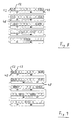
- FIG. 7 shows a two-dimensional array arrangement of pixel elements 41, which are represented by the programmable elements 42 can be selected or activated or deactivated.
- a horizontal shift register 48 is assigned to each pixel line 47 of the array.
- a row decoder 50 and a column decoder 51 serve to address the programmable elements 42. After programming, only the selected pixels in a serial data stream on one or more video lines read out.
- FIG. 8 schematically shows the array reading using the interlaced method.
- the Reading always in the same direction.
- the array of Selected pixel elements 52 are activated by programming, see above that there is a V-shaped active pixel arrangement.
- FIG. 9 shows an array readout which is meandering line by line. The alternates Reading direction line by line, so that after passing through a shift register 48, the subsequent shift register is traversed in the opposite direction. Here too selected pixel elements 52 are activated, corresponding to a preset one Interest region ROI.
- FIGS. 8 and 9 the selected pixel elements 52 are shown dark, so that the V-shaped region of interest is recognizable on the image sensor.
- the number of Video lines can be adapted to the requirements of the application. As a general rule becomes the video line for the differential readout of the PMD signals as a two-wire system be executed.
- the invention provides a 3-D range finder, in particular according to the PMD principle, with a detector line or a detector array
- Programmable pixels can be equipped, and the application-specific Pixel selection is done in particular by programming and an optional one Programming the pixel is possible.
- the addressing can be done in interlaced lines or meandering line by line, and the Detector signals are from the 3D range finder via one or more video lines led out.
- the detector line or the detector array can, depending on the requirements of the respective If necessary, an application-specific, irregular PMD pixel arrangement exhibit.
- Pixel addressing can be sequential or optional, with sequential addressing the order of the pixels selected application-specific can be.
- the invention enables the recording of 3-D distance images with the help of a silicon image sensor, in which the position of the pixels in the focal plane the positions of characteristic features within the scene to be recorded are adjusted.
- a complex one Scene with known features can be analyzed in real time.
- the necessary for this Image recorders are simple and inexpensive. Instead of pixels from a detector line or one Detector arrays are to be arranged regularly and across the board with high density present invention only a few pixel elements for detecting the characteristic Scene features are provided, with the few pixel elements either fixed can be, or by appropriate programming an activation or Deactivation of individual pixels from a large number of pixels can be done.
- a particularly fast, sequential image reading process takes place in the shift register.
- dynamic reprogramming of the pixels during detector operation is flexible Pixel selection possible.
- the invention enables fast 3-D Pattern recognition through scene-adapted pixel arrangement.
- Head position of the occupants are determined in order to be the one to be emitted in an airbag Adjust the gas quantity individually to the head position and thus the risk of injury reduce. Furthermore, an out-of-position sensor system is possible, with one camera Driver and front passenger watched to determine position.
- Precrash sensor technology offers a further possible application Distance image sensor is automatically recorded very quickly, whether people or Objects are present in the vicinity of the vehicle to be subsequently placed in the Intervene vehicle functions, for example by braking, or by triggering a warning function.
- the range finder according to the invention and the Procedure for obstacle detection for example in stop and go traffic, the vehicle in front is observed and when a minimum distance is reached, e.g. is dependent on the respective driving state, braking takes place.
- the present invention can also be part of an interior surveillance system be, for example, to detect a change in condition in the vehicle and an alarm trigger. This can be done with just a few picture elements in a cost-effective manner Monitoring of the vehicle interior takes place, in particular for theft protection. A wide variety of applications are also possible, for example in Automation, manufacturing technology, and other fields.
Landscapes
- Physics & Mathematics (AREA)
- General Physics & Mathematics (AREA)
- Engineering & Computer Science (AREA)
- Theoretical Computer Science (AREA)
- Length Measuring Devices By Optical Means (AREA)
Abstract
Description
Einschränkungen oder mit einem unverhältnismäßig großen Aufwand und hohen Kosten möglich.
- Fig. 1
- eine PMD-Detektorzeile mit unregelmäßiger Pixelanordnung, als erste bevorzugte Ausführungsform der Erfindung;
- Fig. 2
- ein PMD-Detektorarray mit einer V-förmigen Interesseregion bzw. Region of Interest (ROI) als eine weitere Ausführungsform der Erfindung;
- Fig. 3
- ein PMD-Detektorarray mit einer kreuzförmigen Interesseregion gemäß einer noch weiteren Ausführungsform der Erfindung;
- Fig. 4
- ein PMD-Array mit wahlfreier Adressierung;
- Fig. 5
- ein PMD-Array mit sequentieller Adressierung;
- Fig. 6
- eine PMD-Detektorzeile mit Pixelprogrammierung gemäß einer anderen bevorzugten Ausführungsform der Erfindung;
- Fig. 7
- die Architektur eines PMD-Arrays mit programmierbaren Pixeln;
- Fig. 8
- eine Array-Auslesung im Zeilensprungverfahren; und
- Fig. 9
- eine Array-Auslesung, die zeilenweise mäandrierend erfolgt.
Claims (19)
- Bildaufnehmer, insbesondere zur dreidimensionalen Erfassung von Objekten oder Szenen, mit
einer Detektoreinheit (10;20; 30; 40), die eine Vielzahl von photoempfindlichen Pixelelementen (21; 31; 41; 52) umfasst, zur Erzeugung von Signalen, die Informationen über einzelne Bildpunkte enthalten, und
einem Signalausgang (34, 35), dem die Signale der Pixelelemente (21; 31; 41; 52) zugeführt werden, zur Ausgabe von Bildinformationen,
dadurch gekennzeichnet, dass
die zur Bildinformation beitragenden Pixelelemente (21; 31; 41; 52) unregelmäßig angeordnet sind, und/oder in ihrer Anordnung an zu erwartende Positionen charakteristischer Bildelemente angepasst oder anpassbar sind. - Bildaufnehmer nach Anspruch 1, dadurch gekennzeichnet, dass die Pixelelemente (21; 31; 41; 52) direkt adressierbar sind
- Bildaufnehmer nach Anspruch 1 oder 2, dadurch gekennzeichnet, dass die Pixelelemente (21; 31; 41; 52) sequentiell oder wahlfrei adressierbar sind
- Bildaufnehmer nach einem der vorhergehenden Ansprüche, dadurch gekennzeichnet, dass die Adressierung der Pixelelemente (21; 31; 41; 52) in einer vorbestimmten Reihenfolge erfolgt oder wählbar ist.
- Bildaufnehmer nach einem der vorhergehenden Ansprüche, dadurch gekennzeichnet, dass die zur Bildinformation beitragenden Pixelelemente (21) V-förmig oder kreuzförmig angeordnet sind.
- Bildaufnehmer nach einem der vorhergehenden Ansprüche, dadurch gekennzeichnet, dass die Pixelelemente (41) programmierbar sind, um ausgewählte Pixelelemente (41) zu aktivieren oder zu deaktivieren.
- Bildaufnehmer nach einem der vorhergehenden Ansprüche, gekennzeichnet durch programmierbare Elemente (42) zur Auswahl von Pixelelementen (41).
- Bildaufnehmer nach einem der vorhergehenden Ansprüche, gekennzeichnet durch Schalter zur Überbrückung von Pixeln und/oder zum Unterbrechen von Adressleitungen.
- Bildaufnehmer nach einem der vorhergehenden Ansprüche, gekennzeichnet durch schmelzbare elektrische Verbindungen zur permanenten Aktivierung oder Deaktivierung einzelner Pixelelemente (21; 31; 41; 52).
- Bildaufnehmer nach einem der Ansprüche 7 bis 9, gekennzeichnet durch einen Zeilendecoder (50) und/oder einen Spaltendecoder (51), zur Adressierung der programmierbaren Elemente (42).
- Bildaufnehmer nach einem der vorhergehenden Ansprüche, gekennzeichnet durch ein Schieberegister (48) zur Auslesung der zur Bildinformation beitragenden oder ausgewählten Pixelelemente (41).
- Bildaufnehmer nach einem der vorhergehenden Ansprüche, gekennzeichnet durch ein oder mehrere Videoleitungen (35) zur Ausgabe der Signale der Pixelelemente (21; 31; 41; 52).
- Bildaufnehmer nach einem der vorhergehenden Ansprüche, gekennzeichnet durch Photonic Mixer Devices zur Erfassung dreidimensionaler Entfernungsbilder.
- Bildaufnahmeverfahren, insbesondere zur dreidimensionalen Erfassung von Objekten oder Szenen, bei dem mittels photoempfindlicher Pixelelemente (21; 31; 41; 52) Signale erzeugt werden, die Informationen über einzelne Bildpunkte enthalten,
und anschließend die Signale als Bildinformationen bereitgestellt werden,
dadurch gekennzeichnet, dass
die bereitgestellten Signale Bildpunkten entsprechen, die in ihrer Anordnung an zu erwartende Positionen charakteristischer Bildelemente angepasst sind, und/oder die unregelmäßig angeordnet sind. - Bildaufnahmeverfahren nach Anspruch 14, dadurch gekennzeichnet, dass die Adressierung der Pixelelemente (21; 31; 41; 52) sequentiell oder wahlfrei erfolgt.
- Bildaufnahmeverfahren nach Anspruch 14 oder 15, dadurch gekennzeichnet, dass die bei der Adressierung der Pixelelemente (21; 31; 41; 52) die Reihenfolge anwendungsspezifisch gewählt wird.
- Bildaufnahmeverfahren nach einem der Ansprüche 14 bis 16, dadurch gekennzeichnet, dass eine Adressierung der Pixelelemente (21; 31; 41; 52) im Zeilensprung oder zeilenweise mäandrierend erfolgt
- Bildaufnahmeverfahren nach einem der Ansprüche 14 bis 17, dadurch gekennzeichnet, dass die Pixelelemente (41) programmiert werden, um ausgewählte Pixelelemente (41) zu aktivieren und/oder zu deaktivieren.
- Bildaufnahmeverfahren nach einem der Ansprüche 14 bis 18, dadurch gekennzeichnet, dass während der Aufnahme eine dynamische Reprogrammierung der Pixelelemente (41) durchgeführt wird.
Applications Claiming Priority (2)
| Application Number | Priority Date | Filing Date | Title |
|---|---|---|---|
| DE2000122454 DE10022454B4 (de) | 2000-05-09 | 2000-05-09 | Bildaufnehmer und Bildaufnahmeverfahren, insbesondere zur dreidimensionalen Erfassung von Objekten und Szenen |
| DE10022454 | 2000-05-09 |
Publications (2)
| Publication Number | Publication Date |
|---|---|
| EP1160725A2 true EP1160725A2 (de) | 2001-12-05 |
| EP1160725A3 EP1160725A3 (de) | 2002-04-03 |
Family
ID=7641239
Family Applications (1)
| Application Number | Title | Priority Date | Filing Date |
|---|---|---|---|
| EP01109802A Withdrawn EP1160725A3 (de) | 2000-05-09 | 2001-04-20 | Bildaufnehmer und Bildaufnahmeverfahren, insbesondere zur dreidimensionalen Erfassung von Objekten oder Szenen |
Country Status (2)
| Country | Link |
|---|---|
| US (1) | US20010052939A1 (de) |
| EP (1) | EP1160725A3 (de) |
Cited By (2)
| Publication number | Priority date | Publication date | Assignee | Title |
|---|---|---|---|---|
| WO2003029839A1 (de) * | 2001-09-27 | 2003-04-10 | Conti Temic Microelectronic Gmbh | Verfahren zur dreidimensionalen erfassung von objekten oder szenen |
| WO2012098117A3 (de) * | 2011-01-18 | 2012-10-04 | Fraunhofer-Gesellschaft zur Förderung der angewandten Forschung e.V. | Bildsensor, bildaufnahmesystem und verfahren zum aufnehmen eines bildes |
Families Citing this family (7)
| Publication number | Priority date | Publication date | Assignee | Title |
|---|---|---|---|---|
| US8251397B2 (en) * | 2000-10-20 | 2012-08-28 | Joseph Akwo Tabe | Advanced weight responsive supplemental restraint computer system |
| US7034873B2 (en) * | 2001-06-29 | 2006-04-25 | Vanguard International Semiconductor Corporation | Pixel defect correction in a CMOS active pixel image sensor |
| US9135483B2 (en) * | 2011-09-09 | 2015-09-15 | Metrologic Instruments, Inc. | Terminal having image data format conversion |
| DE102014106854A1 (de) * | 2014-05-15 | 2016-01-28 | Odos Imaging Ltd. | Bildgebendes System und Verfahren zum Überwachen eines Sichtfeldes |
| IL233711B (en) * | 2014-07-17 | 2018-04-30 | Rafael Advanced Defense Systems Ltd | Object detection system |
| CN105450924B (zh) * | 2014-09-30 | 2019-04-12 | 北京智谷技术服务有限公司 | 超分辨率图像的获取方法和装置 |
| US10304312B2 (en) * | 2015-10-28 | 2019-05-28 | Kyocera Corporation | Imaging apparatus, imaging system, target person monitoring system and control method of imaging apparatus |
Family Cites Families (7)
| Publication number | Priority date | Publication date | Assignee | Title |
|---|---|---|---|---|
| US6445884B1 (en) * | 1995-06-22 | 2002-09-03 | 3Dv Systems, Ltd. | Camera with through-the-lens lighting |
| EP0846391A1 (de) * | 1995-08-22 | 1998-06-10 | Universite Laval | Vorrichtung und verfahren zur adressierung bestimmter zellen eines halbleitersensors |
| DE19613394C1 (de) * | 1996-04-03 | 1997-10-02 | Siemens Ag | Bildaufnahmesystem und Verfahren zur Bildaufnahme |
| EP0809395A3 (de) * | 1996-05-22 | 1998-03-18 | Eastman Kodak Company | CMOS APS mit Matrix-Adressierung und einer kompakten Pixelperiode |
| DE19704496C2 (de) * | 1996-09-05 | 2001-02-15 | Rudolf Schwarte | Verfahren und Vorrichtung zur Bestimmung der Phasen- und/oder Amplitudeninformation einer elektromagnetischen Welle |
| JPH10257396A (ja) * | 1997-03-06 | 1998-09-25 | Toshiba Corp | エリア分離型固体撮像装置 |
| GB2332585B (en) * | 1997-12-18 | 2000-09-27 | Simage Oy | Device for imaging radiation |
-
2001
- 2001-04-20 EP EP01109802A patent/EP1160725A3/de not_active Withdrawn
- 2001-05-09 US US09/852,302 patent/US20010052939A1/en not_active Abandoned
Cited By (2)
| Publication number | Priority date | Publication date | Assignee | Title |
|---|---|---|---|---|
| WO2003029839A1 (de) * | 2001-09-27 | 2003-04-10 | Conti Temic Microelectronic Gmbh | Verfahren zur dreidimensionalen erfassung von objekten oder szenen |
| WO2012098117A3 (de) * | 2011-01-18 | 2012-10-04 | Fraunhofer-Gesellschaft zur Förderung der angewandten Forschung e.V. | Bildsensor, bildaufnahmesystem und verfahren zum aufnehmen eines bildes |
Also Published As
| Publication number | Publication date |
|---|---|
| EP1160725A3 (de) | 2002-04-03 |
| US20010052939A1 (en) | 2001-12-20 |
Similar Documents
| Publication | Publication Date | Title |
|---|---|---|
| DE69232732T2 (de) | Messeinrichtung für sich bewegende Körper und Bildverarbeitungsanordnung zum Messen des Verkehrsflusses | |
| EP1267178B1 (de) | Verfahren zur Verarbeitung eines tiefenaufgelösten Bildes | |
| EP1418444B1 (de) | Verfahren zur Bestimmung einer Eigenbewegung eines Fahrzeugs | |
| DE4410406C2 (de) | Optoelektronische Vorrichtung zum Überwachen der Umgebung eines Fahrzeugs | |
| DE102004010197B4 (de) | Verfahren zur Funktionskontrolle einer Positionsermittlungs- oder Umgebungserfassungseinrichtung eines Fahrzeugs oder zur Kontrolle einer digitalen Karte | |
| DE69302975T2 (de) | Fahrzeugpositionserfassungsanlage auf einer Spur | |
| DE102006010735B4 (de) | Fahrzeugumgebungsüberwachungsvorrichtung | |
| DE102004035842B4 (de) | Duales ungleichartiges erfassendes Objektdetektions- und Zielerfassungssystem | |
| EP1240533B1 (de) | Verfahren zur optischen überwachung der umgebung eines sich bewegenden fahrzeugs | |
| EP2394234B1 (de) | Verfahren und vorrichtung zum ermitteln einer geltenden fahrspurmarkierung | |
| DE112012001318B4 (de) | Redundante Objektdetektion für Fahrerassistenzsysteme | |
| EP1303768B1 (de) | Verfahren zur sichtweitenbestimmung | |
| EP1589484A1 (de) | Verfahren zur Erkennung und/oder Verfolgung von Objekten | |
| DE10246228A1 (de) | Vorrichtung zum Überwachen eines an ein Fahrzeug angrenzenden Bereichs | |
| EP1567888B1 (de) | Verfahren zur erfassung der vorausliegenden umgebung eines strassenfahrzeugs mittels eines umgebungserfassungssystems | |
| DE10102884A1 (de) | Seitenüberwachungsvorrichtung für ein Kraftfahrzeug | |
| DE19842827B4 (de) | Precrashsensierungssystem | |
| DE69825525T2 (de) | Vorrichtung zur Erstellung eines Bildes sowie Verfahren und Vorrichtung zur Entfernungsmessung | |
| DE10022454B4 (de) | Bildaufnehmer und Bildaufnahmeverfahren, insbesondere zur dreidimensionalen Erfassung von Objekten und Szenen | |
| WO2010103061A1 (de) | Vorrichtung und verfahren zur detektion mindestens eines objektes | |
| WO2020020654A1 (de) | Verfahren zum betreiben eines fahrerassistenzsystems mit zwei erfassungseinrichtungen | |
| DE102006010295B4 (de) | Kamerasystem mit zumindest zwei Bildaufnehmern | |
| WO2009077445A1 (de) | Verfahren und vorrichtung zum optischen erfassen einer fahrzeugumgebung | |
| DE69211925T2 (de) | Entfernungsmesser für Abstand zwischen Fahrzeugen mit Nachführung des vorausfahrenden Fahrzeugs | |
| DE10049366A1 (de) | Verfahren zum Überwachen eines Sicherheitsbereichs und entsprechendes System |
Legal Events
| Date | Code | Title | Description |
|---|---|---|---|
| PUAI | Public reference made under article 153(3) epc to a published international application that has entered the european phase |
Free format text: ORIGINAL CODE: 0009012 |
|
| AK | Designated contracting states |
Kind code of ref document: A2 Designated state(s): DE ES FR GB IT SE Kind code of ref document: A2 Designated state(s): AT BE CH CY DE DK ES FI FR GB GR IE IT LI LU MC NL PT SE TR |
|
| AX | Request for extension of the european patent |
Free format text: AL;LT;LV;MK;RO;SI |
|
| PUAL | Search report despatched |
Free format text: ORIGINAL CODE: 0009013 |
|
| AK | Designated contracting states |
Kind code of ref document: A3 Designated state(s): AT BE CH CY DE DK ES FI FR GB GR IE IT LI LU MC NL PT SE TR |
|
| AX | Request for extension of the european patent |
Free format text: AL;LT;LV;MK;RO;SI |
|
| RIC1 | Information provided on ipc code assigned before grant |
Free format text: 7G 06T 1/00 A, 7G 01B 11/02 B, 7H 04N 3/15 B |
|
| RAP1 | Party data changed (applicant data changed or rights of an application transferred) |
Owner name: CONTI TEMIC MICROELECTRONIC GMBH |
|
| 17P | Request for examination filed |
Effective date: 20020424 |
|
| AKX | Designation fees paid |
Free format text: DE ES FR GB IT SE |
|
| 17Q | First examination report despatched |
Effective date: 20030930 |
|
| STAA | Information on the status of an ep patent application or granted ep patent |
Free format text: STATUS: THE APPLICATION IS DEEMED TO BE WITHDRAWN |
|
| 18D | Application deemed to be withdrawn |
Effective date: 20040831 |