EP1158679A1 - Procédé et dispositif de contrôle du déphasage entre quatre signaux mutuellement en quadrature de phase - Google Patents
Procédé et dispositif de contrôle du déphasage entre quatre signaux mutuellement en quadrature de phase Download PDFInfo
- Publication number
- EP1158679A1 EP1158679A1 EP01401262A EP01401262A EP1158679A1 EP 1158679 A1 EP1158679 A1 EP 1158679A1 EP 01401262 A EP01401262 A EP 01401262A EP 01401262 A EP01401262 A EP 01401262A EP 1158679 A1 EP1158679 A1 EP 1158679A1
- Authority
- EP
- European Patent Office
- Prior art keywords
- signals
- signal
- delayed
- delay
- quadrature
- Prior art date
- Legal status (The legal status is an assumption and is not a legal conclusion. Google has not performed a legal analysis and makes no representation as to the accuracy of the status listed.)
- Granted
Links
- 238000000034 method Methods 0.000 title claims abstract description 11
- 230000010363 phase shift Effects 0.000 title claims description 20
- 238000002156 mixing Methods 0.000 claims abstract description 15
- 230000007423 decrease Effects 0.000 claims abstract description 10
- 101150106604 SIS2 gene Proteins 0.000 claims abstract description 7
- 229910052710 silicon Inorganic materials 0.000 claims abstract description 6
- 239000010703 silicon Substances 0.000 claims abstract description 6
- 238000001914 filtration Methods 0.000 claims abstract description 5
- 230000010354 integration Effects 0.000 claims abstract description 3
- 102100029721 DnaJ homolog subfamily B member 1 Human genes 0.000 claims abstract 3
- 101000866018 Homo sapiens DnaJ homolog subfamily B member 1 Proteins 0.000 claims abstract 3
- 230000003111 delayed effect Effects 0.000 claims description 113
- 230000001934 delay Effects 0.000 claims description 15
- 239000000203 mixture Substances 0.000 claims description 15
- 238000002955 isolation Methods 0.000 claims description 5
- 238000007493 shaping process Methods 0.000 claims description 3
- 230000003247 decreasing effect Effects 0.000 claims description 2
- 230000001747 exhibiting effect Effects 0.000 claims description 2
- 238000009413 insulation Methods 0.000 abstract description 5
- 238000012986 modification Methods 0.000 abstract 1
- 230000004048 modification Effects 0.000 abstract 1
- 239000000758 substrate Substances 0.000 description 5
- XUIMIQQOPSSXEZ-UHFFFAOYSA-N Silicon Chemical compound [Si] XUIMIQQOPSSXEZ-UHFFFAOYSA-N 0.000 description 4
- 238000012545 processing Methods 0.000 description 4
- 238000005516 engineering process Methods 0.000 description 3
- 235000021183 entrée Nutrition 0.000 description 3
- 101100536354 Drosophila melanogaster tant gene Proteins 0.000 description 2
- 101100502339 Saccharomyces cerevisiae (strain ATCC 204508 / S288c) SFA1 gene Proteins 0.000 description 2
- 240000008042 Zea mays Species 0.000 description 2
- 230000005540 biological transmission Effects 0.000 description 2
- 238000012937 correction Methods 0.000 description 2
- 230000017105 transposition Effects 0.000 description 2
- 238000011282 treatment Methods 0.000 description 2
- 238000012935 Averaging Methods 0.000 description 1
- 241000861223 Issus Species 0.000 description 1
- 101100042407 Saccharomyces cerevisiae (strain ATCC 204508 / S288c) SFB2 gene Proteins 0.000 description 1
- 230000015572 biosynthetic process Effects 0.000 description 1
- 239000003990 capacitor Substances 0.000 description 1
- 239000000969 carrier Substances 0.000 description 1
- 230000006835 compression Effects 0.000 description 1
- 238000007906 compression Methods 0.000 description 1
- 230000001419 dependent effect Effects 0.000 description 1
- 238000013461 design Methods 0.000 description 1
- 238000011161 development Methods 0.000 description 1
- 230000008030 elimination Effects 0.000 description 1
- 238000003379 elimination reaction Methods 0.000 description 1
- 238000012423 maintenance Methods 0.000 description 1
- 238000004519 manufacturing process Methods 0.000 description 1
- 230000010287 polarization Effects 0.000 description 1
- 238000003786 synthesis reaction Methods 0.000 description 1
- 238000012360 testing method Methods 0.000 description 1
Images




Classifications
-
- H—ELECTRICITY
- H03—ELECTRONIC CIRCUITRY
- H03H—IMPEDANCE NETWORKS, e.g. RESONANT CIRCUITS; RESONATORS
- H03H11/00—Networks using active elements
- H03H11/02—Multiple-port networks
- H03H11/16—Networks for phase shifting
- H03H11/22—Networks for phase shifting providing two or more phase shifted output signals, e.g. n-phase output
-
- H—ELECTRICITY
- H03—ELECTRONIC CIRCUITRY
- H03B—GENERATION OF OSCILLATIONS, DIRECTLY OR BY FREQUENCY-CHANGING, BY CIRCUITS EMPLOYING ACTIVE ELEMENTS WHICH OPERATE IN A NON-SWITCHING MANNER; GENERATION OF NOISE BY SUCH CIRCUITS
- H03B27/00—Generation of oscillations providing a plurality of outputs of the same frequency but differing in phase, other than merely two anti-phase outputs
-
- H—ELECTRICITY
- H03—ELECTRONIC CIRCUITRY
- H03L—AUTOMATIC CONTROL, STARTING, SYNCHRONISATION OR STABILISATION OF GENERATORS OF ELECTRONIC OSCILLATIONS OR PULSES
- H03L7/00—Automatic control of frequency or phase; Synchronisation
- H03L7/06—Automatic control of frequency or phase; Synchronisation using a reference signal applied to a frequency- or phase-locked loop
- H03L7/08—Details of the phase-locked loop
- H03L7/081—Details of the phase-locked loop provided with an additional controlled phase shifter
- H03L7/0812—Details of the phase-locked loop provided with an additional controlled phase shifter and where no voltage or current controlled oscillator is used
-
- H—ELECTRICITY
- H03—ELECTRONIC CIRCUITRY
- H03L—AUTOMATIC CONTROL, STARTING, SYNCHRONISATION OR STABILISATION OF GENERATORS OF ELECTRONIC OSCILLATIONS OR PULSES
- H03L7/00—Automatic control of frequency or phase; Synchronisation
- H03L7/06—Automatic control of frequency or phase; Synchronisation using a reference signal applied to a frequency- or phase-locked loop
- H03L7/08—Details of the phase-locked loop
- H03L7/085—Details of the phase-locked loop concerning mainly the frequency- or phase-detection arrangement including the filtering or amplification of its output signal
- H03L7/087—Details of the phase-locked loop concerning mainly the frequency- or phase-detection arrangement including the filtering or amplification of its output signal using at least two phase detectors or a frequency and phase detector in the loop
-
- H—ELECTRICITY
- H03—ELECTRONIC CIRCUITRY
- H03D—DEMODULATION OR TRANSFERENCE OF MODULATION FROM ONE CARRIER TO ANOTHER
- H03D7/00—Transference of modulation from one carrier to another, e.g. frequency-changing
- H03D7/12—Transference of modulation from one carrier to another, e.g. frequency-changing by means of semiconductor devices having more than two electrodes
- H03D7/125—Transference of modulation from one carrier to another, e.g. frequency-changing by means of semiconductor devices having more than two electrodes with field effect transistors
Definitions
- the invention relates to the control of the phase shift between four mutually phase quadrature signals. It applies advantageously but not limited to digital television broadcasting by satellite as defined in the European DVB-S specification (Digital Video Broadcasting-Satellite) based on the standards of M-PEG compression, and using for example to convey information, a digital quadrature modulation, for example a modulation on a large number of orthogonal carriers (modulation OFDM: "Orthogonal Frequency Division Multiplexing").
- OFDM Orthogonal Frequency Division Multiplexing
- the invention thus applies more particularly to synthesizers ("Tuner” in English), in particular of the type with zero intermediate frequency, such as for example those incorporated in satellite receivers with compressed image data decoder ("Set-top box” in English).
- Television signals from a satellite are amplified and converted into a predetermined frequency band (typically 950-2150 MHz) via a satellite dish and a low noise converter located at the focus of the dish.
- a predetermined frequency band typically 950-2150 MHz
- This signal is then sent to the input of the synthesizer of the receiver.
- the purpose of the synthesizer is to select the desired channel and output a baseband signal on the phase channel (channel I) and on the quadrature channel (Q channel).
- This signal is then converted to a signal digital and demodulated.
- Channel decoding processing includes then also a block which distinguishes, typically by means of a majority logic the "0" of the "1", then performs all of the error correction, i.e. typically Viterbi decoding, the deinterlacing, Reed-Solomon decoding, and defatting.
- the channel decoding device outputs packets which are conventionally decoded in a source decoding device conforms to MPEG standards, so as to re-deliver the signals initial audio and video transmitted via satellite.
- the synthesizer is associated with a local oscillator which generates quadrature radio frequency signals. It is essential to control this quadrature as best as possible, because any error in quadrature between the signals from the oscillator and delivered to synthesizer mixers leads to imprecision on decoding digital information received. And, this quadrature control has to take place over the entire frequency range of the signals received. As indicative, the development specifications impose for example a phase shift error which must remain less than a few degrees, for example 3 °.
- the transmission of data between cellphones and base is not continuous but in the form of packages. And, between the transmission of these packets, it is mobile phones can recalibrate the squaring of the local oscillator by injecting for example a test signal.
- phase shifter which is made up of capacitive resistive cells, which requires a very precise matching of the components when making the phase shifter.
- the local oscillator described in this document of the prior art delivers two signals in opposition to phase from which four mutually formed signals are formed quadrature.
- this phase shift error remains also between the two signals in phase opposition delivered by the phase shifter, as well as between the two other signals in phase opposition also delivered by the phase shifter.
- control according to this prior art comprises a single control of the phase shifter, which is very disadvantageous vis-à-vis a elimination of any noise.
- phase shifter which is very disadvantageous vis-à-vis a elimination of any noise.
- the invention aims to provide a solution to these problems.
- An object of the invention is to propose a control of the phase shift between four mutually phase quadrature signals, which is almost insensitive to noise, simple to make and fully integrable on silicon substrate.
- the invention proposes in particular to control the phase shift by means of a phase locked loop fully differential.
- the use of a differential structure makes the device according to the invention particularly insensitive to noise.
- the invention therefore proposes a method for controlling the phase shift between four mutually phase quadrature signals, in which builds from at least a first basic signal (for example a signal considered as reference signal and therefore having a phase considered to be zero) and a second basic signal (by example a signal having a phase of 90 °) in quadrature with respect to the first basic signal and likely to have a quadrature error with respect to this first basic signal, a first pair of signals delayed by a first adjustable delay.
- This first pair of signals delayed has a first signal delayed relative to the first signal basic and a second delayed signal in phase opposition with respect to at the first delayed signal.
- a second pair of delayed signals is also developed by a second adjustable delay, this second pair comprising a third signal delayed compared to the second basic signal and a fourth signal delayed in phase opposition compared to the third delayed signal.
- each of the delays is then continuously adjusted to from two differential signals from direct crossed mixtures or of the two pairs of delayed signals, so as to increase the value of one of the two delays and decrease the value of the other delay until the four almost quadrature delayed signals are obtained, regardless of said quadrature error.
- a direct mixing means that the delayed signals are used directly, while indirect mixing means using signals from these delayed signals, for example shaped signals.
- mixing is carried out directly or indirectly the first pair of delayed signals with the second pair of delayed signals, this second pair acting as that control the mixture, and we mix directly or indirectly the second pair of delayed signals with the first pair of signals delayed, this first pair of delayed signals acting as mixture control.
- the value of the first delay is continuously adjusted from one of the two summed filtered differential signals, while adjusting continuously the value of the second delay from the other signal summed filtered differential, so as to increase the value of one of the two delays and decrease the value of the other delay until you get all four delayed signals almost in quadrature regardless of said quadrature error.
- the two are advantageously integrated summed filtered differential signals, then the adjustment of the value of the delays from these integrated differential signals.
- the integrating filter is isolated from the noise generated during the delay phase of the basic signals.
- one of the outputs of the summing means is connected at the delay command input of one of the delay cells, while the other output of the summation means is connected to the control input delay of the other delay cell, so as to continuously adjust the value of the first delay and the second delay by increasing the value of one of the two delays and decreasing the value of the other delay until obtain the four delayed signals almost in quadrature, regardless of said quadrature error.
- the device also includes means for shaping connected signals between the inputs of the mixers and the outputs of the delay cells.
- Each delay cell advantageously includes a variable load differential comparator.
- each mixer is a passive ring mixer formed by four transistors mounted in ring.
- the device also advantageously comprises a filter active differential integrator with common mode control, connected between the two outputs of the adder and the two control inputs of delay of the two delay cells.
- the device also preferably includes means insulation connected between the outputs of the integrating filter and the two delay control inputs of the two delay cells, these means being able to isolate the integrating filter from the noise generated by the delay cells.
- the device according to the invention is advantageously integrated on silicon.
- the invention also provides a signal receiver digital satellite television, including a device for tuning incorporating a phase shift control device such as defined above.
- the reference RS designates a receiver / decoder satellite ("set-top box" in English) connected to an antenna ANT dish receiving digital television signals, and intended to receive and decode these signals.
- This RS receiver has at its head a device for synthesizer, or tuner, TZIF, intended to select the desired channel among all the channels present in the signal received at the input of signal from this tuner.
- a device for synthesizer, or tuner, TZIF intended to select the desired channel among all the channels present in the signal received at the input of signal from this tuner.
- This TZIF tuner is of the zero intermediate frequency, i.e. it does not transposition of frequency to an intermediate frequency but does not has only one frequency transposition stage, comprising here MXA and MXB mixers, and directly transposing the signal to vicinity of the baseband of a channel.
- the TZIF tuner has a low noise amplifier at the top variable LNA gain connected between the antenna and the MXA mixers and MXB.
- An LO oscillator delivers basic signals, theoretically at minus two basic phase quadrature signals (having example respectively a zero phase and a 90 ° phase), and in practice four mutually phase quadrature signals. These basic signals are delivered to a phase shift control device IQPLL which consists of a phase locked loop with structure differential.
- This phase locked loop delivers, as we will see in more detail below, at the mixer MXA two signals phase opposition differentials (respectively presenting a phase zero and a 180 ° phase), and delivers two more to the MXB mixer signals in phase opposition, but in phase quadrature with respect to to the two signals delivered to the MXA mixer.
- the processing route comprising the MXA mixer is therefore here the reference route (route I), while the treatment route containing the MXB mixer is the quadrature channel (Q channel).
- channel I represents the signal in phase
- channel Q represents the quadrature signal
- MXA and MXB mixers are equipped with filters outlet low-pass whose cut-off frequency is for example a band bandwidth of the order of 150 to 250 MHz.
- the output signal from both mixers MXA and MXB is therefore a signal centered around the frequency 0 MHz, extending over a frequency band from 150 to 250 MHz and with the selected channel and the channels immediately adjacent.
- the width of a channel being of the order of 40 MHz for high definition digital television signals, the two filters in FPBA0 and FPBB0 baseband, which follow the two mixers MXA and MXB, have a bandwidth of around 40 MHz. Consequently, we finds a filtered signal at the output of these two baseband filters with only the selected channel.
- the two digital quadrature signals I and Q delivered by analog-to-digital converters are processed in a block of BT calculations capable of performing the subsequent conventional treatments of channel demodulation and decoding such as Viterbi decoding, a deinterlacing, Reed-Solomon decoding, clearing, so as to deliver a stream of packets which will be decoded in a block of source decoding according to the MPEG standard, for example.
- FIG. 2 Reference is now made more particularly to FIG. 2 to describe in more detail the IQPLL phase shift control device.
- This IQPLL device which is actually a locking loop of phase with fully differential structure, receives from a local oscillator of conventional structure and known per se, four signals of base mutually in phase quadrature. More specifically, the first basic signal is the signal S0, which is the reference signal in phase (zero phase). The second basic signal is signal S90, which is a signal in quadrature phase (90 °) with respect to the first basic signal S0. This second basic signal S90 is likely to present an error quadrature with respect to the first basic signal, taking into account technological characteristics of the local oscillator.
- the third basic signal here is the signal S180, substantially in phase opposition (phase equal to 180 °) with respect to the first signal basic S0.
- the fourth basic signal here is the signal S270, substantially in phase opposition with respect to the second basic signal S90.
- the two basic signals S0 and S180 (channel I or signal I) are delivered to the two inputs EA1 and EA2 of a first delay cell DLA, on the structure of which we will return in more detail below.
- This first delay cell has a delay command input ECA.
- This first delay cell is capable of delivering on its two outputs SA1 and SA2, a first pair of delayed signals SR0 and SR180, these signals SR0 and SR180 being delayed by a first adjustable delay.
- the first delayed signal SR0 of the first pair of delayed signals is delayed with respect to the first basic signal S0 and the second signal delayed SR180 is out of phase with respect to the first signal delayed SR0.
- the delay is adjusted by the order arriving on the ECA command input.
- the IQPLL loop also includes a second DLB delay cell, with a structure similar to that of the first DLA delay cell.
- This second delay cell receives on its two inputs EB1 and EB2 the two basic signals S90 and S270 (channel Q or signal Q) and delivers a second on its two outputs SB1 and SB2 pair of delayed signals SR90 and SR270, these two signals SR90 and SR270 are delayed by a second adjustable delay.
- the adjustment of this second delay is effected by the command received on the input of ECB command from the DLB cell.
- the third delayed signal SR90 being part of the second delayed signal pair, is delayed relative to the second signal base S90, while the fourth delayed signal SR270 is in opposition phase compared to the third delayed signal SR90.
- the value of the first delay of the first DLA delay cell and the value of the second delay of the second DLB delay cell are continuously adjusted until the four almost quadrature delayed signals are obtained, regardless of the possible quadrature error between the signals of based.
- the two delayed signals SR0 and SR180 which are for example sinusoidal signals, are then shaped in a circuit classic MFA shaping so as to be transformed into square signals (0-1.8 volts for example) SRF0 and SRF180.
- the two delayed signals SR90 and SR270 are transformed into square signals SRF90 and SRF270 by a setting circuit in MFB form.
- the IQPLL loop also includes a first mixer MPA, for example as will be seen in more detail below a mixer passive ring, receiving on two of its inputs EMPA1 and EMPA2 the two signals formatted SRF0 and SRF180, and receiving on two others inputs EMPA3 and EMPA4 the two signals formatted SRF90 and SRF270.
- the first MPA mixer mixes here directly the two signals SRF0 and SRF180 with the two signals SRF90 and SRF270 (indirectly the first pair of delayed signals SR0 and SR180 with the second pair of delayed signals SR90 and SR270) which act as a control of the mixture.
- the MPA mixer then delivers on its two outputs SMPA1 and SMPA2 a first pair of differential signals which is representative of the quadrature error between the first delayed signal SR0 and the third delayed signal SR90.
- the IQPLL loop includes a second mixer MPB, for example with a structure similar to that of the first mixer MPA, which is connected to the outputs of the first and second cells delay. More specifically, this second mixer receives on two of its inputs EMPB1 and EMPB2 the signals formatted SRF90 and SRF270. he also receives on its two other inputs EMPB3 and EMPB4 the signals formatted SRF0 and SRF180.
- This second mixer therefore indirectly mixes the second pair of delayed signals SR90 and SR270 with the first pair of delayed signals SR0 and SR180, which this time acts as mixture control.
- the MPB mixer then delivers on its two SMPB1 and SMPB2 outputs a second pair of differential signals also representative of the quadrature error between the first signal delayed and the third signal delayed.
- the function of the active differential integrator filter FI is integrate each of the differential signals over a predetermined period SDFS1 and SDFS2, so as to increase the level of these signals and adjust more precisely the delay value from these signals integrated SI1 and SI2.
- the two integrated signals SI1 and SI2 are then delivered to an isolation block whose function is to isolate the filter integrator of the noise generated by the DLA and DLB delay cells. And it's from the SIS 1 and SIS2 signals delivered by the isolation block BI which are will adjust the delay value of each delay cell.
- This adjustment will consist in increasing the value of one of the two delays and decrease the value of the other delay until the four delayed signals SR0, SR180, SR90 and SR270 almost in quadrature regardless of said quadrature error.
- the signal SIS 1 coming from the first processing channel (channel I) that the delay of the second DLB delay cell is controlled, while it is with the signal SIS2 coming from the second processing channel (channel Q) that we control the delay of the first DLA delay cell.
- Figure 3 illustrates the structure internal of the DLA cell, it being understood that the DLB cell has a similar structure.
- the two signals SR0 and SR180 delayed will certainly be delayed compared to the signals S180 and S0 respectively, but strictly in phase opposition.
- Such a DLA cell has a variable load differential comparator.
- This differential comparator to variable load here comprises two NMOS transistors TD 1 and TD2, the respective grids form the two inputs EA2 and EA1 of the cell delay.
- the sources of these two transistors are polarized by a source of current SCI.
- the drains of these two transistors are also polarized by two polarization resistors RR1 and RR2.
- the drains of these two transistors respectively form the two outputs SA1 and SA2 of the delay cell.
- the two outputs SA1 and SA2 are respectively connected the grids of two NMOS transistors TT1 and TT2, including the drains and sources are connected together and form the ECA control input of the cell delay.
- Each NMOS transistor is polarized in depletion (English language depletion) in order to present a dependent capacity the level of the SIS2 signal delivered on the ECA control input.
- Level of the SIS2 signal delivered on the ECA control input varies the load (RC product). If the load increases, the gain increases as well as the delay conferred by the first delay cell. If, conversely, the charge decreases, the gain decreases as well as the value of the delay.
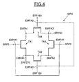
- Figure 4 illustrates the structure of the MPA mixer. It is consisting of four NMOS TA1-TA4 transistors.
- the transistor gate TA1 is connected to the gate of transistor TA3. These two grids form together the EMPA1 input of the mixer.
- the grids of TA2 and TA4 transistors are connected together and form the EMPA2 input of the MPA mixer.
- the source of transistor TA1 is connected to the drain of transistor TA2 and together form the entry EMPA4.
- the source of transistor TA3 is connected to the drain of transistor TA4 and together form the input EMPA3 of the mixer.
- the source of transistor TA4 is connected to the drain of transistor TA1 and together form the output SMPA1, while the source of the transistor TA2 is connected to the drain of transistor TA3 and together form the output SMPA2.
- the average value of the impulse signal delivered to the output SMPA1 is equal to the average value of the pulse signal delivered to the output SMPA2.
- these two mean values are different.
- the structure and function of the MPB mixer, illustrated in FIG. 5, is similar to that which has just been described with reference to the figure 4.
- transistors operating in blocked-on mode it is particularly advantageous to use signals set square form instead of sinusoidal signals.
- Vdd denotes the supply voltage
- Vt denotes the voltage threshold of an NMOS transistor
- the SDFS1 signal and the SDFS2 signal are each representative of the difference between the mean values of the two outputs of the two mixers.
- Each SDFS1 and SDFS2 signal is integrated in the filter active differential integrator of which an example of structure is illustrated on Figure 6.
- This IF filter is a resistive-capacitive integrator filter having example a cutoff frequency of the order of 300 KHz, whose function is to amplify each of the SDFS1 and SDFS2 signals over time.
- This active filter here includes a differential amplifier operational AOP, each output of which is connected to the opposite input by through a capacitor C1, C2.
- resistors R1, R2 are respectively connected between the two inputs of the IF filter and the two inputs of the AOP operational amplifier.
- the active filter FI here comprises means MCMC for controlling common mode. More specifically, these MCMC means include other resistors connected respectively between the two outputs of the AOP amplifier and one of the comparator's (+) inputs. These two resistors have the function of averaging the two outputs of the AOP amplifier.
- the other input (inverting input) of the comparator is connected to the voltage Vdd / 2 via a resistive bridge connected between the voltage Vdd and ground.
- the comparator output controls the charge of the AOP differential operational amplifier.
- MCMC means therefore have the function of setting the mode common output at the voltage Vdd / 2, which allows the Vdd / 2 to be centered delay command value in order to obtain the maximum range of delay cell control.
- This BI block in fact comprises two isolation paths presenting a similar structure.
- Each channel has a T-filter, FT1, FT2.
- This T-filter is a resistive-capacitive filter acting as a low-pass filter seen from the delay cells.
- the device according to the invention makes it possible to correct quadrature errors between basic signals from the oscillator LO, in a range between 0.9 and 2.3 GHz with a possibility maximum phase correction of ⁇ 0.8 ° / 100Mhz.
- the total phase noise at the device output according to the invention is reduced in its closed loop bandwidth by 3 dB on each output signal and the differential phase noise is reduced by 20 dB / decade.
Landscapes
- Digital Transmission Methods That Use Modulated Carrier Waves (AREA)
- Stabilization Of Oscillater, Synchronisation, Frequency Synthesizers (AREA)
Abstract
Description
- un générateur possédant une première sortie pour générer au moins un premier signal de base et une deuxième sortie pour générer au moins un deuxième signal de base en quadrature par rapport au premier signal de base et susceptible de présenter une erreur de quadrature par rapport au premier signal de base, et
- une boucle différentielle à verrouillage de phase comportant :
- une première cellule de retard connectée à la première sortie du générateur et possédant une entrée de commande de retard, cette première cellule de retard étant apte à délivrer une première paire de signaux retardés par un premier retard ajustable, cette première paire de signaux retardés comportant un premier signal retardé par rapport au premier signal de base et un deuxième signal retardé en opposition de phase par rapport au premier signal retardé,
- une deuxième cellule de retard, connectée à la deuxième sortie du générateur et possédant une entrée de commande de retard, cette deuxième cellule de retard étant apte à délivrer une deuxième paire de signaux retardés par un deuxième retard ajustable, cette deuxième paire de signaux retardés comportant un troisième signal retardé par rapport au deuxième signal de base et un quatrième signal retardé en opposition de phase par rapport au troisième signal retardé,
- et des moyens d'ajustement différentiels, connectés entre les sorties des cellules de retards et leurs entrées de commande, et aptes à ajuster continuellement la valeur de chacun des retards à partir de deux signaux différentiels issus de mélanges croisés directs ou indirects des deux paires de signaux retardés, de façon à augmenter la valeur de l'un des deux retards et à diminuer la valeur de l'autre retard jusqu'à obtenir les quatre signaux retardés quasiment en quadrature, indépendamment de ladite erreur de quadrature.
- un premier mélangeur connecté aux sorties de la première et de la deuxième cellules de retard, apte à mélanger directement ou indirectement la première paire de signaux retardés avec la deuxième paire de signaux retardés agissant en tant que commande du mélange, et à délivrer une première paire de signaux différentiels représentative de l'erreur de quadrature entre le premier signal retardé et le troisième signal retardé,
- un deuxième mélangeur connecté aux sorties de la première et de la deuxième cellules de retard, apte à mélanger directement ou indirectement la deuxième paire de signaux retardés avec la première paire de signaux retardés agissant en tant que commande du mélange, et à déliver une deuxième paire de signaux différentiels représentative de l'erreur de quadrature entre le premier signal retardé et le troisième signal retardé,
- un premier filtre passe-bas connecté aux deux sorties du premier mélangeur, un deuxième filtre passe-bas connecté aux deux sorties du deuxième mélangeur et des moyens de sommation connectés aux sorties des deux filtres passe-bas.
- la figure 1 illustre schématiquement un dispositif de synthonisation incorporé dans un récepteur satellite et contenant un dispositif de contrôle de déphasage selon l'invention;
- la figure 2 illustre plus en détail mais toujours schématiquement, la structure interne d'un mode de réalisation d'un dispositif de contrôle de déphasage selon l'invention; et
- les figures 3 à 7 illustrent plus en détail mais toujours schématiquement, certains éléments du dispositif de la figure 2.
Claims (16)
- Procédé de contrôle du déphasage entre quatre signaux mutuellement en quadrature de phase, caractérisé par le fait qu'on élabore à partir d'au moins un premier signal de base (S0) et d'un deuxième signal de base (S90) en quadrature par rapport au premier signal de base et susceptible de présenter une erreur de quadrature par rapport au premier signal de base, une première paire de signaux retardés par un premier retard ajustable comportant un premier signal (SR0) retardé par rapport au premier signal de base (S0) et un deuxième signal retardé (SR180) en opposition de phase par rapport au premier signal retardé, et une deuxième paire de signaux retardés par un deuxième retard ajustable comportant un troisième signal (SR90) retardé par rapport au deuxième signal de base et un quatrième signal retardé (SR270) en opposition de phase par rapport au troisième signal retardé, et on ajuste continuellement la valeur de chacun des retards à partir de deux signaux différentiels (SIS2, SIS1) issus de mélanges croisés directs ou indirects des deux paires de signaux retardés de façon à augmenter la valeur de l'un des deux retards et à diminuer la valeur de l'autre retard jusqu'à obtenir les quatre signaux retardés quasiment en quadrature indépendamment de ladite erreur de quadrature.
- Procédé selon la revendication 1, caractérisé par le fait que dans l'étape d'ajustement, on mélange directement ou indirectement la première paire de signaux retardés (SR0, SR180) avec la deuxième paire de signaux retardés (SR90, SR270) agissant en tant que commande du mélange et on mélange directement ou indirectement la deuxième paire de signaux retardés (SR90, SR270) avec la première paire de signaux retardés (SR0, SR180) agissant en tant que commande du mélange, de façon à obtenir une première paire de signaux différentiels et une deuxième paire de signaux différentiels toutes deux représentatives de l'erreur de quadrature entre le premier signal retardé (SR0) et le troisième signal retardé (SR90), on filtre par un filtrage passe-bas (FA, FB) et on somme les deux paires de signaux différentiels de façon à obtenir une paire de signaux différentiels filtrés sommés (SDFS1, SDFS2) , et on ajuste continuellement la valeur du premier retard à partir de l'un des deux signaux différentiels filtrés sommés tandis qu'on ajuste continuellement la valeur du deuxième retard à partir de l'autre signal différentiel filtré sommé de façon à augmenter la valeur de l'un des deux retards et à diminuer la valeur de l'autre retard jusqu'à obtenir les quatre signaux retardés quasiment en quadrature indépendamment de ladite erreur de quadrature.
- Procédé selon la revendication 1 ou 2, caractérisé par le fait qu'on met en forme (MFA, MFB) les signaux retardés avant mélange.
- Procédé selon l'une des revendications précédentes, caractérisé par le fait qu'on effectue une intégration (FI) des deux signaux différentiels filtrés sommés, et on effectue l'ajustement de la valeur des retards à partir de ces signaux différentiels intégrés (SI1, SI2).
- Procédé selon la revendication 4, caractérisé par le fait qu'on isole le filtre intégrateur (FI) du bruit généré lors de la phase de retardement des signaux de base.
- Procédé selon l'une des revendications précédentes, caractérisé par le fait qu'on élabore les paires de signaux retardés à partir du premier signal de base (S0), du deuxième signal de base (S90), d'un troisième signal de base (S180) sensiblement en opposition de phase par rapport au premier signal de base et d'un quatrième signal de base (S270) sensiblement en opposition de phase par rapport au deuxième signal de base.
- Dispositif de contrôle du déphasage entre quatre signaux mutuellement en quadrature de phase, caractérisé par le fait qu'il comprend un générateur (LO) possédant une première sortie pour générer au moins un premier signal de base (S0) et une deuxième sortie pour générer au moins un deuxième signal de base (S90) en quadrature par rapport au premier signal de base et susceptible de présenter une erreur de quadrature par rapport au premier signal de base, et une boucle différentielle à verrouillage de phase (IQPLL) comportantune première cellule de retard (DLA) connectée à la première sortie du générateur et possédant une entrée de commande de retard, apte à délivrer une première paire de signaux retardés par un premier retard ajustable comportant un premier signal retardé par rapport au premier signal de base et un deuxième signal retardé en opposition de phase par rapport au premier signal retardé,une deuxième cellule de retard (DLB) connectée à la deuxième sortie et possédant une entrée de commande de retard, apte à délivrer une deuxième paire de signaux retardés par un deuxième retard ajustable comportant un troisième signal retardé par rapport au deuxième signal de base et un quatrième signal retardé en opposition de phase par rapport au troisième signal retardé, etdes moyens d'ajustement différentiels, connectés entre les sorties des cellules de retard et leurs entrées de commande, et aptes à ajuster continuellement la valeur de chacun des retards à partir de deux signaux différentiels (SIS2, SIS1) issus de mélanges croisés directs ou indirects des deux paires de signaux retardés, de façon à augmenter la valeur de l'un des deux retards et à diminuer la valeur de l'autre retard jusqu'à obtenir les quatre signaux retardés quasiment en quadrature indépendamment de ladite erreur de quadrature.
- Dispositif selon la revendication 7, caractérisé par le fait que les moyens d'ajustement comportentun premier mélangeur (MPA), connecté aux sorties de la première et de la deuxième cellule de retard, apte à mélanger directement ou indirectement la première paire de signaux retardés avec la deuxième paire de signaux retardés agissant en tant que commande du mélange, et à délivrer une première paire de signaux différentiels représentative de l'erreur de quadrature entre le premier signal retardé et le troisième signal retardé,un deuxième mélangeur (MPB), connecté aux sorties de la première et de la deuxième cellule de retard, apte à mélanger directement ou indirectement la deuxième paire de signaux retardés avec la première paire de signaux retardés agissant en tant que commande du mélange, et à délivrer une deuxième paire de signaux différentiels représentative de l'erreur de quadrature entre le premier signal retardé et le troisième signal retardé,un premier filtre passe-bas (FA) connecté aux deux sorties du premier mélangeur, un deuxième filtre passe-bas (FB) connecté aux deux sorties du deuxième mélangeur, et des moyens de sommation connectés aux sorties des deux filtres passe-bas,et par le fait que l'une des sorties des moyens de sommation est reliée à l'entrée de commande de retard de l'une des cellules de retard, tandis que l'autre sortie des moyens de sommation est reliée à l'entrée de commande de retard de l'autre cellule de retard, de façon à ajuster continuellement la valeur du premier retard et du deuxième retard en augmentant la valeur de l'un des deux retards et en diminuer la valeur de l'autre retard jusqu'à obtenir les quatre signaux retardés quasiment en quadrature indépendamment de ladite erreur de quadrature.
- Dispositif selon la revendication 7 ou 8, caractérisé par le fait qu'il comprend des moyens de mise en forme de signaux (MFA, MFB) connectés entre les entrées des mélangeurs et les sorties des cellules de retard.
- Dispositif selon l'une des revendications 7 à 9, caractérisé par le fait que chaque cellule de retard (DLA, DLB) comporte un comparateur différentiel à charge variable.
- Dispositif selon l'une des revendications 7 à 10, caractérisé par le fait que chaque mélangeur (MPA, MPB) est un mélangeur passif en anneau formé de quatre transistors monté en anneau.
- Dispositif selon l'une des revendications 7 à 11, caractérisé par le fait qu'il comprend un filtre intégrateur différentiel actif (FI) avec contrôle de mode commun (MCMC), connecté entre les deux sorties du sommateur et les deux entrées de commande de retard des deux cellules de retard.
- Dispositif selon la revendication 12, caractérisé par le fait qu'il comprend des moyens d'isolation (BI) connectés entre les sorties du filtre intégrateur et les deux entrées de commande de retard des deux cellules de retard, et aptes à isoler le filtre intégrateur du bruit généré par les cellules de retard.
- Dispositif selon l'une des revendications 7 à 13, caractérisé par le fait que le générateur (LO) est apte à générer sur sa première sortie le premier signal de base et un troisième signal de base sensiblement en opposition de phase par rapport au premier signal de base et à générer sur sa deuxième sortie le deuxième signal de base et un quatrième signal de base sensiblement en opposition de phase par rapport au deuxième signal de base.
- Dispositif selon l'une des revendications 7 à 14, caractérisé par le fait qu'il est intégré sur silicium.
- Récepteur de signaux de télévision numériques par satellite, caractérisé par le fait qu'il comprend un dispositif de synthonisation (TZIF) incorporant un dispositif selon l'une des revendications 7 à 15.
Applications Claiming Priority (2)
| Application Number | Priority Date | Filing Date | Title |
|---|---|---|---|
| FR0006468 | 2000-05-19 | ||
| FR0006468A FR2809266B1 (fr) | 2000-05-19 | 2000-05-19 | Procede et dispositif de controle du dephasage entre quatre signaux mutuellement en quadrature de phase |
Publications (2)
| Publication Number | Publication Date |
|---|---|
| EP1158679A1 true EP1158679A1 (fr) | 2001-11-28 |
| EP1158679B1 EP1158679B1 (fr) | 2005-08-31 |
Family
ID=8850444
Family Applications (1)
| Application Number | Title | Priority Date | Filing Date |
|---|---|---|---|
| EP01401262A Expired - Lifetime EP1158679B1 (fr) | 2000-05-19 | 2001-05-16 | Procédé et dispositif de contrôle du déphasage entre quatre signaux mutuellement en quadrature de phase |
Country Status (4)
| Country | Link |
|---|---|
| US (1) | US6879643B2 (fr) |
| EP (1) | EP1158679B1 (fr) |
| DE (1) | DE60112995D1 (fr) |
| FR (1) | FR2809266B1 (fr) |
Cited By (2)
| Publication number | Priority date | Publication date | Assignee | Title |
|---|---|---|---|---|
| CN101188586B (zh) * | 2006-10-04 | 2011-04-13 | 因芬奈昂技术股份有限公司 | 差分线路补偿装置、方法和系统 |
| EP3116130A1 (fr) * | 2015-07-07 | 2017-01-11 | MediaTek Inc. | Procédé permettant de générer une pluralité de signaux d'oscillation avec différentes phases, circuit associé et oscillateur local |
Families Citing this family (9)
| Publication number | Priority date | Publication date | Assignee | Title |
|---|---|---|---|---|
| US7075585B2 (en) * | 2001-09-17 | 2006-07-11 | Xceive Corporation | Broadband receiver having a multistandard channel filter |
| US7123876B2 (en) * | 2001-11-01 | 2006-10-17 | Motia | Easy set-up, vehicle mounted, in-motion tracking, satellite antenna |
| FR2843249A1 (fr) * | 2002-07-31 | 2004-02-06 | Koninkl Philips Electronics Nv | Recepteur comportant des moyens de reception multiples en parallele. |
| KR100468359B1 (ko) * | 2002-10-31 | 2005-01-27 | 인티그런트 테크놀로지즈(주) | 국부 발진 신호 경로를 통한 동 위상 및 직교 위상 신호간 부정합 보정 회로를 이용한 국부 발진기 및 이를이용한 수신 장치 |
| US6850106B1 (en) * | 2003-07-08 | 2005-02-01 | Mohan Krishna Kunanayagam | Voltage controlled oscillator delay cell |
| CA2460299C (fr) * | 2003-11-28 | 2008-02-12 | Vcom Inc. | Modulation d'amplitude et de phase a l'aide de deux vecteurs a retard numerique |
| CA2460298C (fr) * | 2003-11-28 | 2008-02-12 | Vcom Inc. | Modulation faisant appel au reglage d'amplitude discret et a deux lignes a retard numerique |
| US7755415B2 (en) * | 2006-04-24 | 2010-07-13 | Analog Devices, Inc. | Transistor cell and related circuits and methods |
| EP1881661A1 (fr) * | 2006-07-20 | 2008-01-23 | Abilis Systems Sarl | Procédé et dispositif de traitement d'un signal analogique reçu et pour extraire de données numeriques à partir de celui-ci selon une pluralité de protocoles |
Citations (4)
| Publication number | Priority date | Publication date | Assignee | Title |
|---|---|---|---|---|
| US5060298A (en) * | 1988-12-09 | 1991-10-22 | Siemens Aktiengesellschaft | Monolithic double balanced mixer with high third order intercept point employing an active distributed balun |
| FR2670975A1 (fr) * | 1990-12-21 | 1992-06-26 | Motorola Inc | Appareil et procede de production de signaux en quadrature de phase. |
| US5455543A (en) * | 1994-01-28 | 1995-10-03 | Thomson Consumer Electronics, Inc. | Low power consumption binary phase shift keyed (BPSK) modulator using absorptive electronic switching techniques |
| US5898913A (en) * | 1997-04-25 | 1999-04-27 | Raytheon Company | Plural band converter |
Family Cites Families (6)
| Publication number | Priority date | Publication date | Assignee | Title |
|---|---|---|---|---|
| US3755738A (en) * | 1972-05-01 | 1973-08-28 | Bell Telephone Labor Inc | Passband equalizer for phase-modulated data signals |
| US4358741A (en) * | 1979-09-17 | 1982-11-09 | Ilc Data Device Corporation | Micro time and phase stepper |
| US4794556A (en) * | 1984-09-19 | 1988-12-27 | Massachusetts Institute Of Technology | Method and apparatus for sampling in-phase and quadrature components |
| US5391996A (en) * | 1993-11-19 | 1995-02-21 | General Instrument Corporation Of Delaware | Techniques for generating two high frequency signals with a constant phase difference over a wide frequency band |
| US5796307A (en) * | 1995-11-16 | 1998-08-18 | Ntt Mobile Communications Network Inc. | Amplifying device having input and output nonlinear phase shifters of opposite phase-frequency characteristics |
| KR100304697B1 (ko) * | 1998-11-19 | 2001-09-24 | 윤종용 | 주파수 복조 장치 및 방법 |
-
2000
- 2000-05-19 FR FR0006468A patent/FR2809266B1/fr not_active Expired - Fee Related
-
2001
- 2001-05-16 EP EP01401262A patent/EP1158679B1/fr not_active Expired - Lifetime
- 2001-05-16 DE DE60112995T patent/DE60112995D1/de not_active Expired - Lifetime
- 2001-05-17 US US09/859,731 patent/US6879643B2/en not_active Expired - Lifetime
Patent Citations (4)
| Publication number | Priority date | Publication date | Assignee | Title |
|---|---|---|---|---|
| US5060298A (en) * | 1988-12-09 | 1991-10-22 | Siemens Aktiengesellschaft | Monolithic double balanced mixer with high third order intercept point employing an active distributed balun |
| FR2670975A1 (fr) * | 1990-12-21 | 1992-06-26 | Motorola Inc | Appareil et procede de production de signaux en quadrature de phase. |
| US5455543A (en) * | 1994-01-28 | 1995-10-03 | Thomson Consumer Electronics, Inc. | Low power consumption binary phase shift keyed (BPSK) modulator using absorptive electronic switching techniques |
| US5898913A (en) * | 1997-04-25 | 1999-04-27 | Raytheon Company | Plural band converter |
Cited By (3)
| Publication number | Priority date | Publication date | Assignee | Title |
|---|---|---|---|---|
| CN101188586B (zh) * | 2006-10-04 | 2011-04-13 | 因芬奈昂技术股份有限公司 | 差分线路补偿装置、方法和系统 |
| EP3116130A1 (fr) * | 2015-07-07 | 2017-01-11 | MediaTek Inc. | Procédé permettant de générer une pluralité de signaux d'oscillation avec différentes phases, circuit associé et oscillateur local |
| US10164574B2 (en) | 2015-07-07 | 2018-12-25 | Mediatek Inc. | Method for generating a plurality of oscillating signals with different phases and associated circuit and local oscillator |
Also Published As
| Publication number | Publication date |
|---|---|
| DE60112995D1 (de) | 2005-10-06 |
| US20020051091A1 (en) | 2002-05-02 |
| FR2809266B1 (fr) | 2002-10-11 |
| EP1158679B1 (fr) | 2005-08-31 |
| FR2809266A1 (fr) | 2001-11-23 |
| US6879643B2 (en) | 2005-04-12 |
Similar Documents
| Publication | Publication Date | Title |
|---|---|---|
| EP1259077A1 (fr) | Composant électronique permettant le décodage d'un canal de transmission radiofréquence véhiculant des informations numériques codées, en particulier pour la télédiffusion numérique par satellite | |
| US7298222B2 (en) | Systems and method for automatic quadrature phase imbalance compensation using a delay locked loop | |
| EP0039275B1 (fr) | Dispositif de synthèse et de démodulation combinées pour récepteur d'ondes modulées en fréquence, et récepteur le comportant | |
| EP1158679B1 (fr) | Procédé et dispositif de contrôle du déphasage entre quatre signaux mutuellement en quadrature de phase | |
| FR2835120A1 (fr) | Procede et dispositif de preparation de signaux destines a etre compares pour etablir une pre-distorsion sur l'entree d'un amplificateur | |
| EP2421214A1 (fr) | Récepteur de signaux radiofréquences FSK à faible débit et à conversion directe | |
| FR2681994A1 (fr) | Dispositif de transmission numerique comportant un recepteur a demodulation coherente realisee directement en hyperfrequence. | |
| FR2798019A1 (fr) | Synthetiseur de frequences a boucle de phase | |
| EP1152526B1 (fr) | Synthonisateur du type à fréquence intermédiaire nulle et procédé de commande correspondant | |
| FR2670975A1 (fr) | Appareil et procede de production de signaux en quadrature de phase. | |
| FR2508751A1 (fr) | Recepteur-son d'un televiseur | |
| EP1417750B1 (fr) | Circuit melangeur a rejection de frequence image, notamment pour un recepteur rf a frequence intermediaire nulle ou faible | |
| EP1001548A1 (fr) | Procédé de réglage d'un émetteur récepteur multibande de téléphonie mobile et téléphone mobile ainsi obtenu | |
| EP0800314A1 (fr) | Dispositif de réception de programmes émis par un satellite ou par une station MMDS | |
| FR2853795A1 (fr) | Composant electronique avec dispositif de syntonisation integre, permettant le decodage de signaux de television numerique terrestre ou par cable. | |
| EP1331749A1 (fr) | Transmission de signaux sur un cable coaxial | |
| EP1039628A1 (fr) | Emetteur radiofréquence à fort degré d'intégration et avec annulation d'image, éventuellement auto-calibrée | |
| EP1427099B1 (fr) | Procédé de réduction de la non-linéarité d'ordre deux d'un dispositif de transposition de fréquence et dispositif correspondant | |
| EP0998031A1 (fr) | Amplificateur de courant à faible impédance d'entrée | |
| EP0475162A1 (fr) | Démodulateur hyperfréquence pour liaisons hertziennes numériques utilisant une modulation de type maq | |
| FR2853487A1 (fr) | Composant electronique permettant le decodage de signaux de television numerique par satellite | |
| EP1089427B1 (fr) | Procédé de comparaison des amplitudes de deux signaux électriques | |
| FR2853796A1 (fr) | Composant electronique permettant le decodage de signaux de television numerique terrestre ou par cable. | |
| FR2853486A1 (fr) | Composant electronique permettant le decodage de signaux de television numerique ou par cable | |
| FR2823031A1 (fr) | Dispositif amplificateur a commutation de gain, en particulier pour un telephone mobile cellulaire |
Legal Events
| Date | Code | Title | Description |
|---|---|---|---|
| PUAI | Public reference made under article 153(3) epc to a published international application that has entered the european phase |
Free format text: ORIGINAL CODE: 0009012 |
|
| AK | Designated contracting states |
Kind code of ref document: A1 Designated state(s): AT BE CH CY DE DK ES FI FR GB GR IE IT LI LU MC NL PT SE TR Kind code of ref document: A1 Designated state(s): DE FR GB |
|
| AX | Request for extension of the european patent |
Free format text: AL;LT;LV;MK;RO;SI |
|
| 17P | Request for examination filed |
Effective date: 20020508 |
|
| AKX | Designation fees paid |
Free format text: DE FR GB |
|
| 17Q | First examination report despatched |
Effective date: 20040611 |
|
| GRAP | Despatch of communication of intention to grant a patent |
Free format text: ORIGINAL CODE: EPIDOSNIGR1 |
|
| GRAS | Grant fee paid |
Free format text: ORIGINAL CODE: EPIDOSNIGR3 |
|
| GRAA | (expected) grant |
Free format text: ORIGINAL CODE: 0009210 |
|
| AK | Designated contracting states |
Kind code of ref document: B1 Designated state(s): DE FR GB |
|
| REG | Reference to a national code |
Ref country code: GB Ref legal event code: FG4D Free format text: NOT ENGLISH |
|
| GBT | Gb: translation of ep patent filed (gb section 77(6)(a)/1977) |
Effective date: 20050831 |
|
| REF | Corresponds to: |
Ref document number: 60112995 Country of ref document: DE Date of ref document: 20051006 Kind code of ref document: P |
|
| PG25 | Lapsed in a contracting state [announced via postgrant information from national office to epo] |
Ref country code: DE Free format text: LAPSE BECAUSE OF FAILURE TO SUBMIT A TRANSLATION OF THE DESCRIPTION OR TO PAY THE FEE WITHIN THE PRESCRIBED TIME-LIMIT Effective date: 20051201 |
|
| PLBE | No opposition filed within time limit |
Free format text: ORIGINAL CODE: 0009261 |
|
| STAA | Information on the status of an ep patent application or granted ep patent |
Free format text: STATUS: NO OPPOSITION FILED WITHIN TIME LIMIT |
|
| 26N | No opposition filed |
Effective date: 20060601 |
|
| PGFP | Annual fee paid to national office [announced via postgrant information from national office to epo] |
Ref country code: GB Payment date: 20070427 Year of fee payment: 7 |
|
| PGFP | Annual fee paid to national office [announced via postgrant information from national office to epo] |
Ref country code: FR Payment date: 20070529 Year of fee payment: 7 |
|
| GBPC | Gb: european patent ceased through non-payment of renewal fee |
Effective date: 20080516 |
|
| REG | Reference to a national code |
Ref country code: FR Ref legal event code: ST Effective date: 20090119 |
|
| PG25 | Lapsed in a contracting state [announced via postgrant information from national office to epo] |
Ref country code: FR Free format text: LAPSE BECAUSE OF NON-PAYMENT OF DUE FEES Effective date: 20080602 |
|
| PG25 | Lapsed in a contracting state [announced via postgrant information from national office to epo] |
Ref country code: GB Free format text: LAPSE BECAUSE OF NON-PAYMENT OF DUE FEES Effective date: 20080516 |