EP1158581A1 - Method for manufacturing soi wafer, and soi wafer - Google Patents
Method for manufacturing soi wafer, and soi wafer Download PDFInfo
- Publication number
- EP1158581A1 EP1158581A1 EP00966464A EP00966464A EP1158581A1 EP 1158581 A1 EP1158581 A1 EP 1158581A1 EP 00966464 A EP00966464 A EP 00966464A EP 00966464 A EP00966464 A EP 00966464A EP 1158581 A1 EP1158581 A1 EP 1158581A1
- Authority
- EP
- European Patent Office
- Prior art keywords
- wafer
- heat treatment
- soi
- wafers
- layer
- Prior art date
- Legal status (The legal status is an assumption and is not a legal conclusion. Google has not performed a legal analysis and makes no representation as to the accuracy of the status listed.)
- Granted
Links
Images
Classifications
-
- H—ELECTRICITY
- H10—SEMICONDUCTOR DEVICES; ELECTRIC SOLID-STATE DEVICES NOT OTHERWISE PROVIDED FOR
- H10P—GENERIC PROCESSES OR APPARATUS FOR THE MANUFACTURE OR TREATMENT OF DEVICES COVERED BY CLASS H10
- H10P90/00—Preparation of wafers not covered by a single main group of this subclass, e.g. wafer reinforcement
- H10P90/19—Preparing inhomogeneous wafers
- H10P90/1904—Preparing vertically inhomogeneous wafers
- H10P90/1906—Preparing SOI wafers
- H10P90/1914—Preparing SOI wafers using bonding
- H10P90/1916—Preparing SOI wafers using bonding with separation or delamination along an ion implanted layer, e.g. Smart-cut
-
- H—ELECTRICITY
- H10—SEMICONDUCTOR DEVICES; ELECTRIC SOLID-STATE DEVICES NOT OTHERWISE PROVIDED FOR
- H10P—GENERIC PROCESSES OR APPARATUS FOR THE MANUFACTURE OR TREATMENT OF DEVICES COVERED BY CLASS H10
- H10P95/00—Generic processes or apparatus for manufacture or treatments not covered by the other groups of this subclass
- H10P95/90—Thermal treatments, e.g. annealing or sintering
-
- H—ELECTRICITY
- H10—SEMICONDUCTOR DEVICES; ELECTRIC SOLID-STATE DEVICES NOT OTHERWISE PROVIDED FOR
- H10W—GENERIC PACKAGES, INTERCONNECTIONS, CONNECTORS OR OTHER CONSTRUCTIONAL DETAILS OF DEVICES COVERED BY CLASS H10
- H10W10/00—Isolation regions in semiconductor bodies between components of integrated devices
- H10W10/10—Isolation regions comprising dielectric materials
- H10W10/181—Semiconductor-on-insulator [SOI] isolation regions, e.g. buried oxide regions of SOI wafers
-
- Y—GENERAL TAGGING OF NEW TECHNOLOGICAL DEVELOPMENTS; GENERAL TAGGING OF CROSS-SECTIONAL TECHNOLOGIES SPANNING OVER SEVERAL SECTIONS OF THE IPC; TECHNICAL SUBJECTS COVERED BY FORMER USPC CROSS-REFERENCE ART COLLECTIONS [XRACs] AND DIGESTS
- Y10—TECHNICAL SUBJECTS COVERED BY FORMER USPC
- Y10S—TECHNICAL SUBJECTS COVERED BY FORMER USPC CROSS-REFERENCE ART COLLECTIONS [XRACs] AND DIGESTS
- Y10S438/00—Semiconductor device manufacturing: process
- Y10S438/977—Thinning or removal of substrate
Definitions
- the present invention relates to a method for producing an SOI (Silicon On Insulator) wafer, more specifically, a method for producing an SOI wafer by the so-called hydrogen ion delamination method (also called Smart Cut Method (registered trademark)) comprising bonding an ion-implanted wafer to another wafer that serves as a substrate and then delaminating the wafers to produce an SOI wafer, in which surface roughness is improved by a heat treatment after the delamination, and an SOI wafer produced by the method. Further, the present invention also relates to a method for producing an SOI wafer that can reduce bonding failures during the production of the SOI wafer and can provide SOI wafers with good yield, in which a heat treatment is performed after the delamination.
- SOI Silicon On Insulator
- This method is a technique for producing an SOI wafer, wherein an oxide layer is formed on at least one of two silicon wafers, at least either hydrogen ions or rare gas ions are implanted into one wafer from its top surface to form a micro bubble layer (enclosed layer) in this silicon wafer, then the ion-implanted surface of the wafer is bonded to the other silicon wafer via the oxide layer, thereafter.
- the wafers were subjected to a heat treatment (delamination heat treatment) to delaminate one of the wafer as a thin film at the micro bubble layer as a cleavage plane, and the other wafer is further subjected to a heat treatment (bonding heat treatment) to obtain an SOI wafer in which an SOI layer is firmly bonded on the silicon wafer (refer to Japanese Patent Laid-open (Kokai) Publication No. 5-211128).
- a heat treatment laminate heat treatment
- bonding heat treatment bonding heat treatment
- the SOI layer surface as it is after the delamination at the micro bubble layer as a cleavage plane has higher surface roughness compared with a mirror-polished wafer used for usual device production, and therefore the wafer as it is cannot be used for the device production. Accordingly, in order to improve the aforementioned surface roughness, polishing using a small amount of stock removal for polishing, which is called touch polish, is usually performed.
- the SOI layer is extremely thin, and therefore when its surface is polished, there is caused a problem that variation in SOI layer thickness becomes large due to fluctuation of the polishing amount within the surface.
- Japanese Patent Laid-open (Kokai) Publication No. 10-242154 discloses a method wherein, after a second heat treatment for strengthening bonding of a support substrate and a single crystal silicon thin film (bonding heat treatment), a third heat treatment is performed at a temperature of 1000-1300°C for 10 minutes to 5 hours in a hydrogen atmosphere to improve average surface roughness of the silicon thin film.
- Japanese Patent Laid-open (Kokai) Publication No. 10-275905 discloses a method for producing an SOI wafer wherein a wafer of the SOI structure having a delaminated surface, which is obtained by the hydrogen ion delamination method, is subjected to annealing in a hydrogen atmosphere (hydrogen annealing) to flatten the delaminated surface.
- any of the techniques disclosed in the aforementioned patent documents utilizes a heat treatment in a hydrogen atmosphere to improve the surface roughness of a delaminated wafer.
- the aforementioned Japanese Patent Laid-open (Kokai) Publication No. 10-242154 defines temperature and time for the third heat treatment (hydrogen annealing) for improving the average surface roughness.
- the SOI layer single crystal silicon thin film
- CZ method Czochralski method
- COP Crystal Originated Particle
- a heat treatment performed in an argon atmosphere also improves the surface roughness like the heat treatment in hydrogen, however, it also cannot obviate the problem of etching through COP. That is, it is known that a CZ wafer has crystal defects called COPs introduced therein during the crystal growth, and it has become clear that, if such a CZ wafer is utilized for the bond wafer to be a device active layer, COPs exist also in the SOI layer and in a case of an extremely thin SOI layer, which is required in recent years, the COPs penetrate the SOI layer and form pinholes to markedly degrade electric characteristics.
- Japanese Patent Laid-open (Kokai) Publication No. 10-275905 discloses that, as specific methods for the heat treatment (annealing), the heat treatment can be performed by any one of short time annealing (rapid thermal anneal, RTA) of the single wafer processing in which wafer is treated one by one and plasma annealing, besides the method of hydrogen annealing performed for several tens of seconds to several tens of minutes. in a hydrogen atmosphere using a batch processing type furnace.
- RTA rapid thermal anneal
- the rapid thermal annealing (RTA) utilizing a rapid heating/rapid cooling apparatus can be performed within an extremely short period of time. Therefore, it was considered that the aforementioned buried oxide layer was not etched, COPs in the SOI layer could be eliminated simultaneously, and thus the surface roughness could be improved efficiently.
- the present invention was accomplished in order to solve the aforementioned problems, and its object is to improve surface roughness over the range from short period to long period of an SOI layer surface delaminated by the hydrogen ion delamination method without polishing and to secure its thickness uniformity, as well as to efficiently produce SOI wafers free from generation of pits due to COPs in SOI layers with high throughput.
- the present invention provides a method for producing an SOI wafer by the hydrogen ion delamination method comprising at least a step of bonding a base wafer and a bond wafer having a micro bubble layer formed by gas ion implantation and a step of delaminating a wafer having an SOI layer at the micro bubble layer as a border, wherein, after the delamination step, the wafer having an SOI layer is subjected to a two-stage heat treatment in an atmosphere containing hydrogen or argon utilizing a rapid heating/rapid cooling apparatus and a batch processing type furnace.
- a wafer having an SOI layer is subjected to a heat treatment consisting of two stages utilizing separately a rapid heating/rapid cooling apparatus and a batch processing type furnace after the delamination as described above, surface crystallinity is restored and the surface roughness of short periods is improved in the heat treatment by the rapid heating/rapid cooling apparatus, and the surface roughness of long periods can be improved by the heat treatment utilizing the batch processing type furnace.
- the wafers can be produced with higher throughput compared with a case where wafers are subjected to a heat treatment for a long period of time by the single wafer processing in a rapid heating/rapid cooling apparatus.
- the two-stage heat treatment is preferably performed by subjecting the wafers to a heat treatment in the rapid heating/rapid cooling apparatus and then a heat treatment in the batch processing type furnace.
- both of the short period components and long period components of surface roughness are improved by the two-stage heat treatment as described above. If the heat treatment in the rapid heating/rapid cooling apparatus for a short period of time is performed as the first stage, crystallinity of the surface is restored and COPs in the SOI layer are markedly reduced. Therefore, when the heat treatment by the batch processing type furnace is performed in a subsequent stage, COPs in the SOI layer are substantially eliminated already. Accordingly, even if the heat treatment is performed for a relatively long period of time, the etching of the buried oxide layer by hydrogen gas or argon gas, which is caused through penetrated COPs, is suppressed, and thus pits are not generated.
- the present invention also provides a method for producing an SOI wafer by the hydrogen ion delamination method comprising at least a step of bonding a base wafer and a bond wafer having a micro bubble layer formed by gas ion implantation and a step of delaminating a wafer having an SOI layer at the micro bubble layer as a border, wherein an FZ wafer, an epitaxial wafer or a CZ wafer of which COPs at least on surface are reduced is used as the bond wafer, and the wafer having an SOI layer is subjected to a heat treatment under an atmosphere containing hydrogen or argon in a batch processing type furnace after the delamination step.
- an SOI wafer is produced by using any one of an FZ wafer, an epitaxial wafer and a CZ wafer of which COPs at least on surface are reduced is used as the bond wafer as described above, COPs in the SOI layer can be reduced or substantially completely eliminated. Therefore, the problem of etching of the buried oxide layer due to COPs is not caused, and a heat treatment at a high temperature for a long period of time in a batch processing type furnace also becomes possible.
- Another object of the present invention is to provide SOI wafers with good yield by reducing bonding failures such as voids and blisters generated at a bonding surface, when SOI wafers of which COPs in the SOI layer are reduced are produced as described above.
- the present invention also provides a method characterized by using a CZ wafer produced from a single crystal ingot of which COPs are reduced for the whole crystal as a wafer used for the bond wafer.
- a CZ wafer produced from a single crystal ingot of which COPs are reduced for the whole crystal is used as described above, a usual mirror-polished surface can be used as a bonding surface, and therefore bonding failures can be reduced compared with a case utilizing an epitaxial wafer.
- the method since the method utilizes a CZ wafer, it can be applied to a wafer having a large diameter such as 200 mm, 300 mm or a further larger diameter, which are considered difficult to be produced for FZ wafers.
- COPs are reduced for the whole crystal (whole wafer)
- the stock removal of the delaminated plane for polishing is not required to be limited, when the delaminated wafer is recycled as a bond wafer.
- the surface roughness of the SOI layer can be reduced without producing pits of the buried oxide layer.
- an SOI wafer which is produced by the aforementioned method, characterized in that the wafer has an RMS (root mean square roughness) value of 0.5 nm or less concerning surface roughness for both of 1 ⁇ m square and 10 ⁇ m square.
- both of the short period components (for example, about 1 ⁇ m square) and the long period components (for example, about 10 ⁇ m square) of the surface roughness of the SOI layer are improved, and both of RMS values therefor are very small, i.e., 0.5 nm or less, which means surface roughness comparable to that of mirror-polished wafers.
- the film thickness does not become uneven unlike in a case where the surface is polished. Therefore, such an SOI wafer can suitably be used for the production of recent highly integrated devices.
- the short period components of surface roughness are improved within an extremely short period of time by the heat treatment using an RTA apparatus, and in addition, a lot of wafers can be processed at one time and the long period components are improved in a batch processing type furnace. Therefore, the heat treatment can be efficiently performed as a whole, and thus SOI wafers of superior surface characteristics can be produced at a low cost.
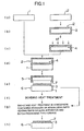
- Fig. 1 (a) to (h) show a flow diagram of an exemplary process for producing an SOI wafer by the hydrogen ion delamination method according to the present invention.
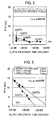
- Fig. 2 shows a graph representing relationship among RTA treatment temperature, treatment time, and P-V value for 1 ⁇ m square.
- Fig. 3 shows a graph representing relationship among RTA treatment temperature, treatment time, and P-V value for 10 ⁇ m square.
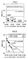
- Fig. 4 shows a graph representing relationship among RTA treatment temperature, treatment time, and RMS value for 1 ⁇ m square.
- Fig. 5 shows a graph representing relationship among RTA treatment temperature, treatment time, and RMS value for 10 ⁇ m square.
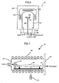
- Fig. 6 is a schematic view showing an exemplary rapid heating/rapid cooling apparatus.
- Fig. 7 is a schematic view showing another exemplary rapid heating/rapid cooling apparatus.
- Fig. 1 shows a flow diagram of an exemplary process for producing an SOI wafer by the hydrogen ion delamination method according to the present invention.
- the present invention will be explained hereafter mainly as for a case where two of silicon wafers are bonded.
- two mirror-surface silicon wafers are prepared first in the step (a). That is, a base wafer 1 that serves as a substrate and a bond wafer 2 from which an SOI layer is obtained, which correspond to specifications of devices, are prepared.
- step (b) at least one of the wafers, the bond wafer 2 in this case, is subjected to thermal oxidation to form an oxide layer 3 having a thickness of about 0.1-2.0 ⁇ m on its surface.
- step (c) at least either hydrogen ions or rare gas ions, hydrogen ions in this case, are implanted into one surface of the bond wafer 2 on which surface the oxide layer was formed to form a micro bubble layer (enclosed layer) 4 parallel to the surface in mean penetrating depth of the ions.
- the ion implantation temperature is preferably 25-450°C.
- the step (d) is a step of superimposing the base wafer 1 on the hydrogen ion implanted surface of the hydrogen ion implanted bond wafer 2 via an oxide layer and bonding them. By contacting the surfaces of two of the wafers to each other in a clean atmosphere at an ordinary temperature, the wafers are adhered to each other without using an adhesive or the like.
- the subsequent step (e) is a delamination heat treatment step in which the wafers were delaminated at the enclosed layer 4 as a border to separate them into a delaminated wafer 5 and a wafer 6 having an SOI layer (SOI layer 7 + buried oxide layer 3 + base wafer 1).
- the wafers are subjected to a heat treatment at a temperature of about 500°C or more under an inert gas atmosphere, the wafers are separated into the delaminated wafer 5 and the wafer 6 having an SOI layer due to rearrangement of crystals and aggregation of bubbles (this wafer may be simply called SOI wafer hereinafter including such a wafer subjected to a heat treatment).
- the method of the present invention is the same as the conventional hydrogen ion delamination method.
- the method is characterized by subjecting the wafer 6 having an SOI layer 7 to a two-stage heat treatment in an atmosphere containing hydrogen or argon using a rapid heating/rapid cooling apparatus and a batch processing type furnace (step (g)), after the delamination heat treatment step (e).
- the atmosphere containing hydrogen or argon may consist of 100% of hydrogen, 100% of argon or a mixed gas of hydrogen and argon.
- the bonding heat treatment may be performed in the step (f) like a conventional method. Since the bonding strength of the wafers brought into close contact in the aforementioned bonding step (d) and the delamination heat treatment step (e) as it is would be weak for use in the device production process, the wafer 6 having an SOI layer is subjected to a heat treatment at a high temperature as a bonding heat treatment in this step (f) to obtain sufficient bonding strength.
- This heat treatment is preferably performed, for example, at 1050°C to 1200°C for 30 minutes to 2 hours under an inert gas atmosphere.
- the wafer 6 having an SOI layer is subjected to the bonding heat treatment as required, and then subjected to the two-stage heat treatment in an atmosphere containing hydrogen or argon using a rapid heating/rapid cooling apparatus and a batch processing type furnace.
- the two-stage heat treatment using a rapid heating/rapid cooling apparatus and a batch processing type furnace according to the present. invention may also serve as the bonding heat treatment.
- the heat treatment using a rapid heating/rapid cooling apparatus is preferably performed first, in particular, when a usual CZ wafer having a lot of COPs is used as a bond wafer.
- a CZ wafer contains COPs introduced during the crystal production as described above. Therefore, when the SOI layer is thin as required in recent years, the COPs may exist while penetrating the SOI layer to form pinholes. In such a case, if the wafer is subjected to a heat treatment in an atmosphere containing hydrogen or argon over a long period of time in a batch processing type furnace, hydrogen gas or argon gas may penetrate through the pinholes and etch the buried oxide layer 3 to form pits during the heat treatment.
- an SOI wafer excellent in both of the short period components and long period components of surface roughness can be obtained by subjecting the wafer to a heat treatment at a temperature of about 1000-1300°C for 10 minutes to about 5 hours in a batch processing type furnace, while avoiding the problem of etching of the buried oxide layer, as in the case of performing the two-stage heat treatment.
- Examples of the CZ wafer of which COPs at least on surface are reduced include a CZ wafer produced from a single crystal ingot of which COPs are reduced for the whole crystal by changing a usual CZ single crystal pulling rate (about 1 mm/min) to a pulling rate of, for example, 0.6 mm/min or lower, a CZ wafer produced from a single crystal ingot of which grown-in defects such as COPs are reduced for the whole crystal by controlling V/G (V: pulling rate, G: temperature gradient along the direction of solid-liquid interface of crystal), or a CZ wafer produced with usual pulling conditions and subjected to a heat treatment in an atmosphere of hydrogen, argon or the like to reduce COPs contained in at least a region of wafer surface to be an SOI layer, and so forth.
- V/G pulling rate
- G temperature gradient along the direction of solid-liquid interface of crystal
- an epitaxial wafer, FZ wafer or CZ wafer subjected to hydrogen (argon) annealing may be used.
- an epitaxial layer is deposited on a surface of usual mirror-polished wafer, and its surface roughness (haze level) is degraded compared with a usual mirror-polished surface. Furthermore, projections called mounds and the like may be generated on the surface. Therefore, if such a surface is bonded, bonding failures called voids or blisters are likely to occur due to the influence of the degraded surface roughness or protrusions. Therefore, there may be used a measure of slightly polishing the epitaxial layer and then using it for bonding.
- the bond wafer after the delamination is recycled as a bond wafer, the delaminated plane must be polished before use.
- an epitaxial wafer suffers from a problem that, if the stock removal for polishing becomes large, the epitaxial layer may be removed. Therefore, it is necessary to take a countermeasure such as depositing the epitaxial layer with a sufficiently large thickness beforehand or making the stock removal for polishing small. This problem is similarly applied to a wafer of which COPs are reduced only in the vicinity of the wafer surface, like a CZ wafer subjected to hydrogen (argon) annealing.
- the stock removal for polishing is not limited for recycling at all, and the wafer can be recycled for a plurality of times.
- a CZ wafer produced from a single crystal ingot of which COPs are reduced for the whole crystal is advantageous in view of the possibility of the production of wafers having a larger diameter.
- the maximum diameter of wafers currently produced on commercial level is 150 mm, and it is extremely difficult to obtain wafers having a diameter of 200 mm, 300 mm or a further larger diameter.
- those having a diameter of 300 mm are already mass-produced, and study for production of those having a further larger diameter is also progressing. Therefore, it is well possible to meet the demand for a larger diameter.
- the production of SOI wafers by the hydrogen ion delamination method using CZ wafers produced from a single crystal ingot of which COPs are reduced for the whole crystal as bond wafers is the only method that simultaneously has three kinds of advantages, i.e., reduction of bonding failures, reuse of bond wafers and usability for wafers of a large diameter.
- the heat treatment performed in an atmosphere containing hydrogen or argon using a rapid heating/rapid cooling apparatus can be performed in a temperature range of 1000°C to the melting point or lower of silicon for 1-300 seconds.
- a wafer having an SOI layer after the delamination By subjecting a wafer having an SOI layer after the delamination to a heat treatment in an atmosphere containing hydrogen or argon using a rapid heating/rapid cooling apparatus, crystallinity of the SOI layer surface can be efficiently restored in an extremely short period of time, surface roughness, in particular, short period components thereof (about 1 ⁇ m square) can be improved, and COPs in the SOI layer can also be markedly reduced.
- the heat treatment can be performed more effectively in a temperature range of 1200-1350°C.
- Examples of such an apparatus that can rapidly heat and rapidly cool an SOI wafer in an atmosphere containing hydrogen or argon, which is used in the present invention, include apparatuses such as lamp heaters based on heat radiation.
- apparatuses such as lamp heaters based on heat radiation.
- SHS-2800 produced by AST Corp. can be mentioned. These apparatuses are not particularly complicated, and are not expensive either.
- Fig. 6 is a schematic view of an apparatus capable of rapid heating and rapid cooling.
- the heat treatment apparatus 20 shown in Fig. 6 has a bell jar 21 composed of, for example, silicon carbide or quartz, and a wafer is heattreated in this bell jar 21. Heating is performed by heaters 22 and 22', which are disposed so that they should surround the bell jar 21. These heaters are each constituted by an upper heater and a lower heater which are separated from each other, so that electric power supplied to each of them can be independently controlled. Of course, the heating mechanism is not limited to this, and the so-called radiant heating, radiofrequency heating and so forth may also be used.
- a housing 23 for shielding heat is disposed outside the heaters 22 and 22'.
- a water cooled chamber 24 and a base plate 25 are disposed under a furnace, and they shut the inside of the bell jar 21 off from the outer air.
- An SOI wafer 28 is held on a stage 27, and the stage 27 is fixed at the top of supporting shaft 26 which can be freely moved upward and downward by a motor 29.
- the water cooled chamber 24 has a wafer insertion port (not shown in the figure) which can be opened and closed by a gate valve, so that the wafer can be loaded into and unloaded from the furnace along the transverse direction.
- the base plate 25 is provided with a gas inlet and exhaust outlet, so that the gaseous atmosphere in the furnace can be controlled.
- the heat treatment of an SOI wafer for rapid.heating and rapid cooling in an atmosphere containing hydrogen or argon is performed as follows.
- the inside of the bell jar 21 is heated to a desired temperature, for example, 1000°C to the melting point of silicon, by the heaters 22 and 22', and maintained at that temperature.
- a desired temperature for example, 1000°C to the melting point of silicon
- the heat treatment temperature can be selected by changing the position of the stage 27, i.e., the length of the supporting shaft 26 inserted into the furnace.
- the atmosphere for the heat treatment is controlled by introducing an atmospheric gas containing hydrogen or argon through a gas inlet of a base plate 25.
- an SOI wafer is inserted from the insertion port of the water cooled chamber 24 by a wafer handling apparatus not shown in the figure, which is disposed at an adjacent position of the heat treatment apparatus 20, and placed on the stage 27 waiting at its lowest position via, for example, a SiC boat etc.
- a wafer handling apparatus not shown in the figure, which is disposed at an adjacent position of the heat treatment apparatus 20, and placed on the stage 27 waiting at its lowest position via, for example, a SiC boat etc.
- the stage 27 is immediately elevated to a position of desired temperature of from 1000°C to the melting point of silicon by inserting the supporting shaft 26 into the inside of the furnace by the motor 29 so that the SOI wafer on the stage should be subjected to the high temperature heat treatment.
- the stage moves from its lowest position in the water cooled chamber 24 to the desired temperature position within, for example, only 20 seconds, the SOI wafer will be rapidly heated.
- the wafer having an SOI layer can be subjected to the high temperature heat treatment in an atmosphere containing hydrogen or argon for the time that the wafer is maintained at the heating position.
- a predetermined period of time for example, 1-300 seconds
- the stage 27 is immediately descended by pulling the supporting shaft 26 out from the furnace by the motor 29, and positioned at the bottom of the water cooled chamber 24. This descending operation can also be performed within, for example, about 20 seconds. Because the water cooled chamber 24 and the base plate 25 are cooled with water, the wafer having an SOI layer on the stage 27 is cooled rapidly. Finally, the SOI wafer is unloaded by the wafer handling apparatus to finish the heat treatment.
- those wafers can be introduced successively into the apparatus and subjected to the heat treatment, since the temperature in the heat treatment apparatus 20 is not lowered.
- RTA apparatus rapid heating/rapid cooling apparatus
- the heat treatment apparatus 30 shown in Fig. 7 has a chamber 31 consisting of quartz, and a wafer 38 is heat-treated within this chamber 31. Heating is achieved by heating lamps 32, which are disposed under and over the chamber and at left and right of the chamber so that they should surround the chamber 31. Electric power supplied to these lamps 32 can be independently controlled.
- An auto shutter 33 is provided at the gas exhausting side, and it shuts the inside of the chamber 31 off from the outer air.
- the auto shutter 33 has a wafer loading port not shown in the figure, which can be opened and closed by a gate valve.
- the auto shutter 33 is also provided with a gas exhausting outlet, so that the atmosphere in the furnace can be controlled.
- the wafer 38 is placed on a three-point supporting part 35 formed on a quartz tray 34.
- a buffer 36 made of quartz is provided at the gas inlet side of the tray 34, so that it can prevent the wafer 38 from being directly blown by the introduced gas flow.
- the chamber 31 is provided with a special window for temperature measurement, which is not shown in the figure, and the temperature of the wafer 38 can be measured by a pyrometer 37 installed in the outside of the chamber 31 through the special window.
- the heat treatment for rapid heating and rapid cooling of a wafer is performed as follows.
- the wafer 38 is loaded into the chamber 31 from the loading port and placed on the tray 34 by a wafer handling apparatus disposed at an adjacent position of the heat treatment apparatus 30 but not shown in the figure. Then, the auto shutter 33 is closed.
- the heating lamps 32 to heat the wafer 38 to a predetermined temperature, for example, 1100°C to 1300°C. In this operation, it takes, for example, about 20 seconds to attain the desired temperature. Then, the wafer 38 is maintained at the temperature for a predetermined period of time, and thus the wafer 38 can be subjected to a high temperature heat treatment. When the predetermined time has passed and the high temperature heat treatment is finished, output of the lamps is reduced to lower the temperature of the wafer. This temperature decrease can be also performed within, for example, about 20 seconds. Finally, the wafer 38 is unloaded by the wafer handling apparatus to finish the heat treatment.
- a predetermined temperature for example, 1100°C to 1300°C. In this operation, it takes, for example, about 20 seconds to attain the desired temperature.
- the wafer 38 is maintained at the temperature for a predetermined period of time, and thus the wafer 38 can be subjected to a high temperature heat treatment.
- output of the lamps is reduced to lower the temperature of the wafer. This temperature
- the heat treatment by using a rapid heating/rapid cooling apparatus include a method utilizing such an apparatus as shown in Fig. 6, wherein a wafer is immediately loaded into a heat treatment furnace set at a temperature within the aforementioned temperature range, and the wafer is immediately unloaded after the aforementioned heat treatment time has passed, a method utilizing such an apparatus as shown in Fig. 7, wherein a wafer is placed at a predetermined position in a heat treatment furnace and immediately heated by lamp heaters or the like, and so forth.
- RTA apparatus rapid heating/rapid cooling apparatus
- to immediately load and "to immediately unload” mean that there are not employed the conventional temperature increasing and decreasing operations performed over a certain period of time and the so-called loading and unloading operations in which wafers are slowly loaded into and unloaded from a heat treatment furnace. Of course, however, it takes a certain short period of time to transport the wafer to the predetermined position in the furnace, and it takes several seconds to several minutes depending on the performance of a transportation apparatus for loading a wafer.
- the atmosphere for the heat treatment in an atmosphere containing hydrogen or argon according to the present invention may be, for example, 100% hydrogen atmosphere, 100% argon atmosphere or a mixed gas atmosphere of hydrogen and argon.
- batch processing type furnace used herein means a so-called batch type heat treatment furnace of, usually, vertical type or horizontal type, in which a plurality of wafers are placed, hydrogen gas is introduced, temperature is relatively slowly elevated to subject the wafers to a heat treatment at a predetermined temperature for predetermined time, and the temperature is relatively slowly lowered.
- Such an apparatus is capable of heat treatment of a large number of wafers at one time.
- Such an apparatus is also excellent in the controllability of temperature, and hence enables stable operation.
- the heat treatment conditions for the batch processing type furnace are basically the same as those for the aforementioned RTA apparatus except that the heat treatment time becomes longer. It can be performed in 100% hydrogen atmosphere, 100% argon atmosphere or a mixed gas atmosphere of hydrogen and argon at a temperature of from 1000°C to the melting point of silicon, and in particular, it can be performed more effectively at a temperature range of 1200-1350°C.
- the long period components for example, about 10 ⁇ m square
- surface roughness of SOI wafers can be improved over the range from short period to long period, and SOI wafers free from pits generated due to COPs can be obtained, even if CZ wafers are used as bond wafers.
- the heat treatment can be performed more efficiently, and SOI wafers excellent in the surface characteristics can be produced with a high throughput at a low cost.
- the SOI wafer of the present invention produced as described above can be an SOI wafer of which both of RMS values for 1 ⁇ m square and 10 ⁇ m square concerning surface roughness are 0.5 nm or less.
- the SOI wafer of the present invention of which both of RMS values for 1 ⁇ m square and 10 ⁇ m square concerning surface roughness are 0.5 nm or less as described above, has surface roughness substantially comparative to that of mirror-polished wafers over the range from short period to long period and is excellent in the film thickness uniformity. Therefore, it can be preferably used for the production of recent highly integrated devices.
- a wafer 6 having an SOI layer was obtained through delamination of the bond wafer 2 according to the steps (a) to (e) shown in Fig. 1.
- thickness of the SOI layer 7 was made to be 0.4 ⁇ m, and the other major conditions including those for the ion implantation were as follows.
- the wafer 6 having an SOI layer 7 with a thickness of about 0.4 ⁇ m was obtained.
- a delaminated wafer as it is obtained in Fig. 1 (e) i.e., a wafer having an SOI layer not subjected to the two-stage heat treatment according to the present invention at all.
- P-V (Peak to Valley) value and RMS value of its surface (delaminated plane) were measured by atomic force microscopy for 1 ⁇ m square and 10 ⁇ m square.
- the P-V values were 56.53 nm in average for 1 ⁇ m square, and 56.63 nm in average for 10 ⁇ m square.
- the RMS (root mean square roughness) values were 7.21 nm in average for 1 ⁇ m square, and 5.50 nm in average for 10 ⁇ m square.
- the wafer having an SOI layer obtained through the aforementioned steps of (a) to (e) shown in Fig. 1 was subjected to an RTA treatment in a temperature range of 1000°C to 1225°C in an atmosphere containing hydrogen, and then its surface roughness in terms of P-V value and RMS value was measured for 1 ⁇ m square and 10 ⁇ m square by atomic force microscopy.
- Fig. 2 shows a graph representing relationship among the RTA treatment temperature, the treatment time and the P-V value for 1 ⁇ m square.
- This graph shows that the RTA treatment in a temperature range of 1000°C to 1225°C for several seconds to several tens of seconds greatly improved the short period components (1 ⁇ m) of surface roughness compared with the untreated one, and provided P-V values comparable to that of a mirror-polished wafer (PW).
- PW mirror-polished wafer
- Fig. 3 shows a graph representing relationship among the RTA treatment temperature, the treatment time and the P-V value for 10 ⁇ m square. It can be seen that the long period components (10 ⁇ m) of surface roughness were gradually improved as the treatment time became longer, unlike the case of the aforementioned short period components, and, to obtain a P-V value comparable to that of a mirror-polished wafer (PW), although it depended on the treatment temperature, a period of around several thousands of seconds was required even when the treatment was performed at, for example, 1225°C.
- PW mirror-polished wafer
- Figs. 4 and 5 show the measurement results for the short period components (1 ⁇ m) and the long period components (10 ⁇ m) of surface roughness in terms of RMS values, respectively, and they show relationship among the RTA treatment temperature, the treatment time and the RMS value.
- the short period components (about 1 ⁇ m) of surface roughness are greatly improved to a level comparable to that of a mirror-polished wafer by the RTA treatment for an extremely short period of time (several seconds or several tens of seconds), whereas the long period components (about 10 ⁇ m) cannot be made to be at a level comparable to that of a mirror-polished wafer, although it depends on the treatment temperature, unless the heat treatment is performed for a long period of time (several thousands of seconds or more).
- a silicon single crystal ingot was produced by the CZ method with applying a magnetic field, in which the pulling condition (V/G) was controlled to reduce grown-in defects in the crystal.
- This ingot was processed in a conventional manner to produce a mirror-surface CZ wafer (diameter: 200 mm, crystal orientation ⁇ 100>) of which COPs were reduced for the whole crystal (Example 3).
- COPs and haze level on the surface of this wafer were measured by using a surface inspection apparatus (SP-1, produced by KLA/Tencor Co., Ltd.), and it was found that no COP having a diameter of 0.12 ⁇ m or more existed on the surface and the haze level of the mirror surface was about 0.03 ppm in average.
- a CZ mirror-surface wafer (diameter: 200 mm, crystal orientation ⁇ 100>), which was produced from a silicon single crystal ingot pulled with usual pulling condition (pulling rate: 1.2 mm/min), was loaded into an epitaxial growth apparatus to produce an epitaxial wafer having an epitaxial layer with a thickness of 10 ⁇ m at 1125°C (Example 4).
- the number of COPs having a diameter of 0.12 ⁇ m or more existing on the CZ wafer surface before the deposition of the epitaxial layer was about 1000 per wafer in average.
- Haze level of the epitaxial layer surface was about 0.2 ppm in average.
- wafers that can be used in the present invention are not limited to those, and FZ wafers and hydrogen (argon) annealed wafers can also be used.
- the present invention was explained above mainly for the cases of bonding two of semiconductor wafers (silicon wafers), the present invention is not limited to those, and can similarly be applied to cases where a semiconductor wafer and an insulating substrate (for example, substrates of quartz, sapphire, alumina etc.) are directly bonded to produce SOI wafers.
- a semiconductor wafer and an insulating substrate for example, substrates of quartz, sapphire, alumina etc.
Landscapes
- Crystals, And After-Treatments Of Crystals (AREA)
- Element Separation (AREA)
Abstract
Description
| Heat treatment condition | Heat treatment by RTA apparatus | Heat treatment by batch processing type furnace |
| Example 1 | 1225°C, 10 seconds | 1200°C, 1 hour |
| Example 2 | 1200°C, 30 seconds | 1200°C, 1 hour |
| Comparative Example 1 | 1225°C, 10 seconds | None |
| Results of surface roughness measurement | Before heat treatment (RMS: nm) | After heat treatment (RMS: nm) | ||
| 1 µm square | 10 µm square | 1 µm square | 10 µm square | |
| Example 1 | 7.21 | 5.50 | 0.18 | 0.28 |
| Example 2 | 7.50 | 5.80 | 0.20 | 0.30 |
| Comparative Example 1 | 7.45 | 5.75 | 0.21 | 1.60 |
| Before heat treatment (RMS: nm) | After heat treatment (RMS: nm). | |||
| 1 µm square | 10 µm square | 1 µm square | 10 µm square | |
| Example 3 | 7.33 | 5.60 | 0.18 | 0.33 |
| Example 4 | 7.42 | 5.73 | 0.19 | 0.35 |
Claims (6)
- A method for producing an SOI wafer by the hydrogen ion delamination method comprising at least a step of bonding a base wafer and a bond wafer having a micro bubble layer formed by gas ion implantation and a step of delaminating a wafer having an SOI layer at the micro bubble layer as a border, wherein, after the delamination step, the wafer having an SOI layer is subjected to a two-stage heat treatment in an atmosphere containing hydrogen or argon utilizing a rapid heating/rapid cooling apparatus and a batch processing type furnace.
- The method for producing an SOI wafer according to Claim 1, wherein the two-stage heat treatment is performed by subjecting the wafers to a heat treatment in the rapid heating/rapid cooling apparatus and then a heat treatment in the batch processing type furnace.
- A method for producing an SOI wafer by the hydrogen ion delamination method comprising at least a step of bonding a base wafer and a bond wafer having a micro bubble layer formed by gas ion implantation and a step of delaminating a wafer having an SOI layer at the micro bubble layer as a border, wherein an FZ wafer, an epitaxial wafer or a CZ wafer of which COPs at least on surface are reduced is used as the bond wafer, and the wafer having an SOI layer is subjected to a heat treatment under an atmosphere containing hydrogen or argon in a batch processing type furnace after the delamination step.
- A method for producing an SOI wafer by the hydrogen ion delamination method comprising at least a step of bonding a base wafer and a bond wafer having a micro bubble layer formed by gas ion implantation and a step of delaminating a wafer having an SOI layer at the micro bubble layer as a border, wherein a CZ wafer produced from a single crystal ingot of which COPs are reduced for the whole crystal is used as the bond wafer.
- The method for producing an SOI wafer according to Claim 4, wherein the wafer having an SOI layer is subjected to a heat treatment under an atmosphere containing hydrogen or argon in a batch processing type furnace after the delamination step.
- An SOI wafer produced by the method according to any one of Claims 1-3 and 5, which has an RMS value of 0.5 nm or less concerning surface roughness for both of 1 µm square and 10 µm square.
Priority Applications (1)
| Application Number | Priority Date | Filing Date | Title |
|---|---|---|---|
| EP10009285A EP2259299A1 (en) | 1999-10-14 | 2000-10-13 | Method for manufacturing SOI wafer, and SOI wafer |
Applications Claiming Priority (3)
| Application Number | Priority Date | Filing Date | Title |
|---|---|---|---|
| JP29213499 | 1999-10-14 | ||
| JP29213499 | 1999-10-14 | ||
| PCT/JP2000/007111 WO2001028000A1 (en) | 1999-10-14 | 2000-10-13 | Method for manufacturing soi wafer, and soi wafer |
Related Child Applications (1)
| Application Number | Title | Priority Date | Filing Date |
|---|---|---|---|
| EP10009285A Division-Into EP2259299A1 (en) | 1999-10-14 | 2000-10-13 | Method for manufacturing SOI wafer, and SOI wafer |
Publications (3)
| Publication Number | Publication Date |
|---|---|
| EP1158581A1 true EP1158581A1 (en) | 2001-11-28 |
| EP1158581A4 EP1158581A4 (en) | 2010-03-10 |
| EP1158581B1 EP1158581B1 (en) | 2016-04-27 |
Family
ID=17777984
Family Applications (2)
| Application Number | Title | Priority Date | Filing Date |
|---|---|---|---|
| EP00966464.0A Expired - Lifetime EP1158581B1 (en) | 1999-10-14 | 2000-10-13 | Method for producing soi wafer |
| EP10009285A Ceased EP2259299A1 (en) | 1999-10-14 | 2000-10-13 | Method for manufacturing SOI wafer, and SOI wafer |
Family Applications After (1)
| Application Number | Title | Priority Date | Filing Date |
|---|---|---|---|
| EP10009285A Ceased EP2259299A1 (en) | 1999-10-14 | 2000-10-13 | Method for manufacturing SOI wafer, and SOI wafer |
Country Status (5)
| Country | Link |
|---|---|
| US (3) | US6846718B1 (en) |
| EP (2) | EP1158581B1 (en) |
| JP (1) | JP4103391B2 (en) |
| KR (1) | KR100730806B1 (en) |
| WO (1) | WO2001028000A1 (en) |
Cited By (14)
| Publication number | Priority date | Publication date | Assignee | Title |
|---|---|---|---|---|
| FR2827078A1 (en) * | 2001-07-04 | 2003-01-10 | Soitec Silicon On Insulator | METHOD FOR REDUCING SURFACE ROUGHNESS |
| FR2827423A1 (en) * | 2001-07-16 | 2003-01-17 | Soitec Silicon On Insulator | METHOD FOR IMPROVING SURFACE CONDITION |
| RU2217842C1 (en) * | 2003-01-14 | 2003-11-27 | Институт физики полупроводников - Объединенного института физики полупроводников СО РАН | Method for producing silicon-on-insulator structure |
| FR2852143A1 (en) * | 2003-03-04 | 2004-09-10 | Soitec Silicon On Insulator | PREVENTIVE TREATMENT PROCESS FOR THE CROWN OF A MULTILAYERED WAFER |
| EP1469509A4 (en) * | 2002-01-23 | 2006-05-10 | Tokyo Electron Ltd | DEVICE AND METHOD FOR TREATING A SUBSTRATE, AND APPARATUS FOR PRODUCING SEMICONDUCTOR DEVICES |
| WO2007080013A1 (en) * | 2006-01-09 | 2007-07-19 | International Business Machines Corporation | Method and apparatus for treating bonded wafer semiconductor substrates |
| FR2899380A1 (en) * | 2006-03-31 | 2007-10-05 | Soitec Silicon On Insulator | METHOD FOR REVELATING CRYSTALLINE DEFECTS IN A MASSIVE SUBSTRATE |
| US7338883B2 (en) | 2002-07-09 | 2008-03-04 | S.O.I.Tec Silicon On Insulator Technologies | Process for transferring a layer of strained semiconductor material |
| EP1662555A4 (en) * | 2003-09-05 | 2008-07-30 | Sumco Corp | PROCESS FOR PRODUCING SOI PLATEBOARD |
| EP1408551A4 (en) * | 2001-07-17 | 2009-06-17 | Shinetsu Handotai Kk | PROCESS FOR PRODUCING BINDING PADS |
| US7820549B2 (en) | 2004-08-26 | 2010-10-26 | Siltronic Ag | Layered semiconductor wafer with low warp and bow, and process for producing it |
| CN102629556A (en) * | 2011-02-04 | 2012-08-08 | 索泰克公司 | Semi-conductor structure with smooth surface and method for obtaining such a structure |
| EP2802001A4 (en) * | 2012-01-06 | 2015-09-16 | Shinetsu Handotai Kk | METHOD FOR MANUFACTURING SILICON WAFER ON INSULATION (SOI) FIXED |
| WO2020049251A1 (en) * | 2018-09-03 | 2020-03-12 | Soitec | Method for manufacturing a cfet device |
Families Citing this family (47)
| Publication number | Priority date | Publication date | Assignee | Title |
|---|---|---|---|---|
| EP1158581B1 (en) | 1999-10-14 | 2016-04-27 | Shin-Etsu Handotai Co., Ltd. | Method for producing soi wafer |
| US7749910B2 (en) * | 2001-07-04 | 2010-07-06 | S.O.I.Tec Silicon On Insulator Technologies | Method of reducing the surface roughness of a semiconductor wafer |
| US7883628B2 (en) * | 2001-07-04 | 2011-02-08 | S.O.I.Tec Silicon On Insulator Technologies | Method of reducing the surface roughness of a semiconductor wafer |
| CN100403543C (en) * | 2001-12-04 | 2008-07-16 | 信越半导体株式会社 | Bonded wafer and method for manufacturing bonded wafer |
| JP2003204048A (en) * | 2002-01-09 | 2003-07-18 | Shin Etsu Handotai Co Ltd | SOI wafer manufacturing method and SOI wafer |
| US7208396B2 (en) * | 2002-01-16 | 2007-04-24 | Tegal Corporation | Permanent adherence of the back end of a wafer to an electrical component or sub-assembly |
| FR2835095B1 (en) * | 2002-01-22 | 2005-03-18 | PROCESS FOR PREPARING SEPARABLE SEMICONDUCTOR ASSEMBLIES, IN PARTICULAR FOR FORMING SUBSTRATES FOR ELECTRONICS, OPTOELECTRIC, AND OPTICS | |
| FR2835097B1 (en) * | 2002-01-23 | 2005-10-14 | OPTIMIZED METHOD FOR DEFERRING A THIN LAYER OF SILICON CARBIDE ON A RECEPTACLE SUBSTRATE | |
| FR2839385B1 (en) * | 2002-05-02 | 2004-07-23 | Soitec Silicon On Insulator | PROCESS FOR TAKING OFF MATERIAL LAYERS |
| DE60315670T2 (en) * | 2002-07-17 | 2008-06-05 | S.O.I.Tec Silicon On Insulator Technologies | METHOD FOR THE PRODUCTION OF SUBSTRATES, ESPECIALLY FOR OPTICS, ELECTRONICS AND OPTOELECTRONICS |
| TWI233154B (en) * | 2002-12-06 | 2005-05-21 | Soitec Silicon On Insulator | Method for recycling a substrate |
| JP4407127B2 (en) * | 2003-01-10 | 2010-02-03 | 信越半導体株式会社 | Manufacturing method of SOI wafer |
| WO2004095112A2 (en) * | 2003-04-21 | 2004-11-04 | Sioptical, Inc. | Cmos-compatible integration of silicon-based optical devices with electronic devices |
| EP1652230A2 (en) * | 2003-07-29 | 2006-05-03 | S.O.I.Tec Silicon on Insulator Technologies | Method for obtaining a thin high-quality layer by co-implantation and thermal annealing |
| FR2858715B1 (en) * | 2003-08-04 | 2005-12-30 | Soitec Silicon On Insulator | METHOD FOR DETACHING SEMICONDUCTOR LAYER |
| DE60336090D1 (en) * | 2003-12-03 | 2011-03-31 | Soitec Silicon On Insulator | METHOD FOR IMPROVING THE SURFACE WEIGHT OF A SEMICONDUCTOR WAFERS |
| US20050236619A1 (en) * | 2004-04-21 | 2005-10-27 | Vipulkumar Patel | CMOS-compatible integration of silicon-based optical devices with electronic devices |
| EP1605504B1 (en) * | 2004-06-10 | 2011-05-25 | S.O.I. Tec Silicon on Insulator Technologies S.A. | Method for manufacturing a SOI wafer |
| EP1806769B1 (en) * | 2004-09-13 | 2013-11-06 | Shin-Etsu Handotai Co., Ltd. | Soi wafer manufacturing method |
| US7202117B2 (en) * | 2005-01-31 | 2007-04-10 | Freescale Semiconductor, Inc. | Method of making a planar double-gated transistor |
| FR2881573B1 (en) * | 2005-01-31 | 2008-07-11 | Soitec Silicon On Insulator | METHOD OF TRANSFERRING A THIN LAYER FORMED IN A SUBSTRATE HAVING GAPS AMAS |
| US7387946B2 (en) * | 2005-06-07 | 2008-06-17 | Freescale Semiconductor, Inc. | Method of fabricating a substrate for a planar, double-gated, transistor process |
| EP1798764A1 (en) * | 2005-12-14 | 2007-06-20 | STMicroelectronics S.r.l. | Process for manufacturing wafers usable in the semiconductor industry |
| EP1818976A1 (en) * | 2006-02-14 | 2007-08-15 | S.O.I.Tec Silicon on Insulator Technologies | Process for transferring a thin layer formed in a substrate having crystal originated particles (COPs). |
| JP2007294849A (en) * | 2006-03-27 | 2007-11-08 | Seiko Epson Corp | Semiconductor element, semiconductor device and manufacturing method thereof |
| FR2903809B1 (en) | 2006-07-13 | 2008-10-17 | Soitec Silicon On Insulator | THERMAL TREATMENT OF INTERFACE STABILIZATION E COLLAGE. |
| JP5314838B2 (en) * | 2006-07-14 | 2013-10-16 | 信越半導体株式会社 | Method for reusing peeled wafers |
| US20080083611A1 (en) * | 2006-10-06 | 2008-04-10 | Tegal Corporation | High-adhesive backside metallization |
| JP5249511B2 (en) * | 2006-11-22 | 2013-07-31 | 信越化学工業株式会社 | SOQ substrate and method for manufacturing SOQ substrate |
| EP2015354A1 (en) * | 2007-07-11 | 2009-01-14 | S.O.I.Tec Silicon on Insulator Technologies | Method for recycling a substrate, laminated wafer fabricating method and suitable recycled donor substrate |
| CN101796613B (en) * | 2007-09-14 | 2012-06-27 | 株式会社半导体能源研究所 | Semiconductor devices and electronic equipment |
| US7648868B2 (en) * | 2007-10-31 | 2010-01-19 | International Business Machines Corporation | Metal-gated MOSFET devices having scaled gate stack thickness |
| US7811901B1 (en) * | 2007-12-03 | 2010-10-12 | Silicon Genesis Corporation | Method and edge region structure using co-implanted particles for layer transfer processes |
| US7977206B2 (en) * | 2008-01-16 | 2011-07-12 | Semiconductor Energy Laboratory Co., Ltd. | Method for manufacturing SOI substrate using the heat treatment apparatus |
| US20090223628A1 (en) * | 2008-03-07 | 2009-09-10 | Semiconductor Energy Laboratory Co., Ltd. | Manufacturing apparatus of composite substrate and manufacturing method of composite substrate with use of the manufacturing apparatus |
| US20090246385A1 (en) * | 2008-03-25 | 2009-10-01 | Tegal Corporation | Control of crystal orientation and stress in sputter deposited thin films |
| US8808513B2 (en) * | 2008-03-25 | 2014-08-19 | Oem Group, Inc | Stress adjustment in reactive sputtering |
| CN102292810A (en) * | 2008-11-26 | 2011-12-21 | Memc电子材料有限公司 | Method for processing a silicon-on-insulator structure |
| SG166060A1 (en) * | 2009-04-22 | 2010-11-29 | Semiconductor Energy Lab | Method of manufacturing soi substrate |
| US8673703B2 (en) * | 2009-11-17 | 2014-03-18 | International Business Machines Corporation | Fabrication of graphene nanoelectronic devices on SOI structures |
| JP5673180B2 (en) * | 2011-02-14 | 2015-02-18 | 信越半導体株式会社 | Manufacturing method of bonded wafer |
| JP5664592B2 (en) * | 2012-04-26 | 2015-02-04 | 信越半導体株式会社 | Manufacturing method of bonded wafer |
| US10094988B2 (en) * | 2012-08-31 | 2018-10-09 | Micron Technology, Inc. | Method of forming photonics structures |
| JP2016201454A (en) * | 2015-04-09 | 2016-12-01 | 信越半導体株式会社 | Manufacturing method of SOI wafer |
| FR3046877B1 (en) * | 2016-01-14 | 2018-01-19 | Soitec | METHOD FOR SMOOTHING THE SURFACE OF A STRUCTURE |
| JP6500845B2 (en) * | 2016-06-14 | 2019-04-17 | 信越半導体株式会社 | Method of manufacturing bonded wafer |
| US20180033609A1 (en) * | 2016-07-28 | 2018-02-01 | QMAT, Inc. | Removal of non-cleaved/non-transferred material from donor substrate |
Family Cites Families (45)
| Publication number | Priority date | Publication date | Assignee | Title |
|---|---|---|---|---|
| FR2681472B1 (en) | 1991-09-18 | 1993-10-29 | Commissariat Energie Atomique | PROCESS FOR PRODUCING THIN FILMS OF SEMICONDUCTOR MATERIAL. |
| JPH07321120A (en) * | 1994-05-25 | 1995-12-08 | Komatsu Electron Metals Co Ltd | Heat treatment of silicon wafer |
| US5668045A (en) * | 1994-11-30 | 1997-09-16 | Sibond, L.L.C. | Process for stripping outer edge of BESOI wafers |
| US5494849A (en) * | 1995-03-23 | 1996-02-27 | Si Bond L.L.C. | Single-etch stop process for the manufacture of silicon-on-insulator substrates |
| US5937312A (en) * | 1995-03-23 | 1999-08-10 | Sibond L.L.C. | Single-etch stop process for the manufacture of silicon-on-insulator wafers |
| JPH08264552A (en) | 1995-03-24 | 1996-10-11 | Toshiba Ceramics Co Ltd | Silicon wafer manufacturing method |
| US5863832A (en) * | 1996-06-28 | 1999-01-26 | Intel Corporation | Capping layer in interconnect system and method for bonding the capping layer onto the interconnect system |
| KR100296365B1 (en) * | 1996-06-28 | 2001-11-30 | 고지마 마타오 | Heat treatment method of silicon single crystal wafer, heat treatment device and silicon single crystal wafer and manufacturing method thereof |
| US5989981A (en) * | 1996-07-05 | 1999-11-23 | Nippon Telegraph And Telephone Corporation | Method of manufacturing SOI substrate |
| JP3522482B2 (en) | 1997-02-24 | 2004-04-26 | 三菱住友シリコン株式会社 | Method for manufacturing SOI substrate |
| EP0966464B1 (en) | 1997-03-03 | 2003-05-28 | Basilea Pharmaceutica AG | Substituted 2,4-diaminopyrimidines |
| US6403502B1 (en) * | 1997-03-27 | 2002-06-11 | Shin-Etsu Handotai Co., Ltd. | Heat treatment method for a silicon wafer and a silicon wafer heat-treated by the method |
| JPH10275905A (en) * | 1997-03-31 | 1998-10-13 | Mitsubishi Electric Corp | Silicon wafer manufacturing method and silicon wafer |
| MY120036A (en) * | 1997-04-09 | 2005-08-30 | Memc Electronic Materials | Low defect density, self- interstitial dominated silicon. |
| US6191007B1 (en) | 1997-04-28 | 2001-02-20 | Denso Corporation | Method for manufacturing a semiconductor substrate |
| US6251754B1 (en) * | 1997-05-09 | 2001-06-26 | Denso Corporation | Semiconductor substrate manufacturing method |
| JP3412449B2 (en) | 1997-05-29 | 2003-06-03 | 三菱住友シリコン株式会社 | Method for manufacturing SOI substrate |
| US6103599A (en) * | 1997-07-25 | 2000-08-15 | Silicon Genesis Corporation | Planarizing technique for multilayered substrates |
| JP3324469B2 (en) * | 1997-09-26 | 2002-09-17 | 信越半導体株式会社 | Method for producing SOI wafer and SOI wafer produced by this method |
| JP3451908B2 (en) * | 1997-11-05 | 2003-09-29 | 信越半導体株式会社 | SOI wafer heat treatment method and SOI wafer |
| JP2998724B2 (en) * | 1997-11-10 | 2000-01-11 | 日本電気株式会社 | Manufacturing method of bonded SOI substrate |
| JP3407629B2 (en) * | 1997-12-17 | 2003-05-19 | 信越半導体株式会社 | Heat treatment method for silicon single crystal wafer and silicon single crystal wafer |
| JPH11191617A (en) * | 1997-12-26 | 1999-07-13 | Mitsubishi Materials Silicon Corp | Manufacture of soi substrate |
| JPH11307472A (en) * | 1998-04-23 | 1999-11-05 | Shin Etsu Handotai Co Ltd | Method for producing SOI wafer by hydrogen ion stripping method and SOI wafer produced by this method |
| JP3500063B2 (en) * | 1998-04-23 | 2004-02-23 | 信越半導体株式会社 | Method for recycling peeled wafer and silicon wafer for reuse |
| JP3456143B2 (en) * | 1998-05-01 | 2003-10-14 | 信越半導体株式会社 | Laminated materials and optical functional devices |
| JP3697106B2 (en) | 1998-05-15 | 2005-09-21 | キヤノン株式会社 | Method for manufacturing semiconductor substrate and method for manufacturing semiconductor thin film |
| US6224668B1 (en) * | 1998-06-02 | 2001-05-01 | Shin-Etsu Handotai Co., Ltd. | Method for producing SOI substrate and SOI substrate |
| JP3762144B2 (en) * | 1998-06-18 | 2006-04-05 | キヤノン株式会社 | Method for manufacturing SOI substrate |
| JP2000012864A (en) * | 1998-06-22 | 2000-01-14 | Semiconductor Energy Lab Co Ltd | Method for manufacturing semiconductor device |
| JP3395661B2 (en) * | 1998-07-07 | 2003-04-14 | 信越半導体株式会社 | Method for manufacturing SOI wafer |
| JP3358550B2 (en) * | 1998-07-07 | 2002-12-24 | 信越半導体株式会社 | Method for producing SOI wafer and SOI wafer produced by this method |
| JP2000082679A (en) * | 1998-07-08 | 2000-03-21 | Canon Inc | Semiconductor substrate and manufacturing method thereof |
| JP3385972B2 (en) * | 1998-07-10 | 2003-03-10 | 信越半導体株式会社 | Manufacturing method of bonded wafer and bonded wafer |
| WO2000013211A2 (en) * | 1998-09-02 | 2000-03-09 | Memc Electronic Materials, Inc. | Silicon on insulator structure from low defect density single crystal silicon |
| CN1250945A (en) * | 1998-09-04 | 2000-04-19 | 佳能株式会社 | Semiconductor substrate and its mfg. method |
| JP4244411B2 (en) * | 1998-09-14 | 2009-03-25 | 株式会社Sumco | Manufacturing method of silicon epitaxial wafer |
| US6284384B1 (en) * | 1998-12-09 | 2001-09-04 | Memc Electronic Materials, Inc. | Epitaxial silicon wafer with intrinsic gettering |
| US6387829B1 (en) | 1999-06-18 | 2002-05-14 | Silicon Wafer Technologies, Inc. | Separation process for silicon-on-insulator wafer fabrication |
| EP1158581B1 (en) | 1999-10-14 | 2016-04-27 | Shin-Etsu Handotai Co., Ltd. | Method for producing soi wafer |
| KR100577410B1 (en) * | 1999-11-30 | 2006-05-08 | 엘지.필립스 엘시디 주식회사 | X-ray image sensing device and its manufacturing method |
| EP1302985A1 (en) | 2000-05-30 | 2003-04-16 | Shin-Etsu Handotai Co., Ltd | Method for producing bonded wafer and bonded wafer |
| JP2003168690A (en) * | 2001-11-30 | 2003-06-13 | Seiko Epson Corp | Transistor and method of manufacturing transistor |
| US6888658B2 (en) * | 2002-05-31 | 2005-05-03 | Lucent Technologies Inc. | Method and geometry for reducing drift in electrostatically actuated devices |
| JP4192530B2 (en) * | 2002-08-27 | 2008-12-10 | 株式会社Sumco | Manufacturing method of silicon single crystal wafer for particle monitor |
-
2000
- 2000-10-13 EP EP00966464.0A patent/EP1158581B1/en not_active Expired - Lifetime
- 2000-10-13 JP JP2001530120A patent/JP4103391B2/en not_active Expired - Lifetime
- 2000-10-13 EP EP10009285A patent/EP2259299A1/en not_active Ceased
- 2000-10-13 US US09/857,803 patent/US6846718B1/en not_active Expired - Lifetime
- 2000-10-13 WO PCT/JP2000/007111 patent/WO2001028000A1/en not_active Ceased
- 2000-10-13 KR KR1020017007168A patent/KR100730806B1/en not_active Expired - Lifetime
-
2003
- 2003-10-15 US US10/684,874 patent/US20040063298A1/en not_active Abandoned
-
2004
- 2004-09-24 US US10/948,234 patent/US7176102B2/en not_active Expired - Lifetime
Cited By (35)
| Publication number | Priority date | Publication date | Assignee | Title |
|---|---|---|---|---|
| WO2003005434A3 (en) * | 2001-07-04 | 2003-11-06 | Soitec Silicon On Insulator | Method for reducing surface rugosity of a semiconductor slice |
| FR2827078A1 (en) * | 2001-07-04 | 2003-01-10 | Soitec Silicon On Insulator | METHOD FOR REDUCING SURFACE ROUGHNESS |
| CN1321443C (en) * | 2001-07-04 | 2007-06-13 | S·O·I·Tec绝缘体上硅技术公司 | Method for reducing surface rugosity |
| US6962858B2 (en) | 2001-07-04 | 2005-11-08 | S.O.I.Tec Silicon On Insulator Technologies S.A. | Method for reducing free surface roughness of a semiconductor wafer |
| FR2827423A1 (en) * | 2001-07-16 | 2003-01-17 | Soitec Silicon On Insulator | METHOD FOR IMPROVING SURFACE CONDITION |
| WO2003009366A1 (en) * | 2001-07-16 | 2003-01-30 | S.O.I. Tec Silicon On Insulator Technologies | Method for enhancing surface condition of a semiconductor wafer |
| JP2004535685A (en) * | 2001-07-16 | 2004-11-25 | エス.オー.アイ.テック、シリコン、オン、インシュレター、テクノロジーズ | How to improve the surface condition |
| US6903032B2 (en) | 2001-07-16 | 2005-06-07 | S.O.I.Tec Silicon On Insulator Technologies S.A. | Method for preparing a semiconductor wafer surface |
| EP1408551A4 (en) * | 2001-07-17 | 2009-06-17 | Shinetsu Handotai Kk | PROCESS FOR PRODUCING BINDING PADS |
| EP1469509A4 (en) * | 2002-01-23 | 2006-05-10 | Tokyo Electron Ltd | DEVICE AND METHOD FOR TREATING A SUBSTRATE, AND APPARATUS FOR PRODUCING SEMICONDUCTOR DEVICES |
| US7125799B2 (en) | 2002-01-23 | 2006-10-24 | Tokyo Electron Limited | Method and device for processing substrate, and apparatus for manufacturing semiconductor device |
| US8049224B2 (en) | 2002-07-09 | 2011-11-01 | S.O.I.Tec Silicon On Insulator Technologies | Process for transferring a layer of strained semiconductor material |
| US7534701B2 (en) | 2002-07-09 | 2009-05-19 | S.O.I. Tec Silicon On Insulator Technologies | Process for transferring a layer of strained semiconductor material |
| US7803694B2 (en) | 2002-07-09 | 2010-09-28 | S.O.I.Tec Silicon On Insulator Technologies | Process for transferring a layer of strained semiconductor material |
| US7338883B2 (en) | 2002-07-09 | 2008-03-04 | S.O.I.Tec Silicon On Insulator Technologies | Process for transferring a layer of strained semiconductor material |
| RU2217842C1 (en) * | 2003-01-14 | 2003-11-27 | Институт физики полупроводников - Объединенного института физики полупроводников СО РАН | Method for producing silicon-on-insulator structure |
| US6939783B2 (en) | 2003-03-04 | 2005-09-06 | S.O.I.Tec Silicon On Insulator Technologies, S.A. | Preventive treatment method for a multilayer semiconductor wafer |
| US7190029B2 (en) | 2003-03-04 | 2007-03-13 | S.O.I.Tec Silicon On Insulator Technologies S.A. | Preventive treatment method for a multilayer semiconductor wafer |
| WO2004079801A1 (en) * | 2003-03-04 | 2004-09-16 | S.O.I.Tec Silicon On Insulator Technologies | Preventive treatment process for the ring of a multilayer wafer |
| KR100806981B1 (en) * | 2003-03-04 | 2008-02-25 | 에스. 오. 이. 떼끄 씰리꽁 오 냉쉴라또흐 떼끄놀로지 | Preventive treatment process for the ring of a multilayer wafer |
| FR2852143A1 (en) * | 2003-03-04 | 2004-09-10 | Soitec Silicon On Insulator | PREVENTIVE TREATMENT PROCESS FOR THE CROWN OF A MULTILAYERED WAFER |
| US7563697B2 (en) | 2003-09-05 | 2009-07-21 | Sumco Corporation | Method for producing SOI wafer |
| EP1662555A4 (en) * | 2003-09-05 | 2008-07-30 | Sumco Corp | PROCESS FOR PRODUCING SOI PLATEBOARD |
| US7820549B2 (en) | 2004-08-26 | 2010-10-26 | Siltronic Ag | Layered semiconductor wafer with low warp and bow, and process for producing it |
| WO2007080013A1 (en) * | 2006-01-09 | 2007-07-19 | International Business Machines Corporation | Method and apparatus for treating bonded wafer semiconductor substrates |
| US7413964B2 (en) | 2006-03-31 | 2008-08-19 | S.O.I.Tec Silicon On Insulator Technologies | Method of revealing crystalline defects in a bulk substrate |
| EP1840560A3 (en) * | 2006-03-31 | 2009-07-01 | S.O.I.Tec Silicon on Insulator Technologies | Method of revealing crystalline faults in a massive substrate |
| FR2899380A1 (en) * | 2006-03-31 | 2007-10-05 | Soitec Silicon On Insulator | METHOD FOR REVELATING CRYSTALLINE DEFECTS IN A MASSIVE SUBSTRATE |
| CN102629556A (en) * | 2011-02-04 | 2012-08-08 | 索泰克公司 | Semi-conductor structure with smooth surface and method for obtaining such a structure |
| FR2971361A1 (en) * | 2011-02-04 | 2012-08-10 | Soitec Silicon On Insulator | SEMICONDUCTOR STRUCTURE WITH A SMOOTHED SURFACE AND METHOD OF OBTAINING SUCH A STRUCTURE |
| EP2485249A3 (en) * | 2011-02-04 | 2013-07-03 | Soitec | Semi-conductor structure with smooth surface and method for obtaining such a structure |
| US8492877B2 (en) | 2011-02-04 | 2013-07-23 | Soitec | Semiconductor structure with smoothed surface and process for obtaining such a structure |
| CN102629556B (en) * | 2011-02-04 | 2015-11-18 | 索泰克公司 | There is the semiconductor structure of smooth surface and the process for obtaining this structure |
| EP2802001A4 (en) * | 2012-01-06 | 2015-09-16 | Shinetsu Handotai Kk | METHOD FOR MANUFACTURING SILICON WAFER ON INSULATION (SOI) FIXED |
| WO2020049251A1 (en) * | 2018-09-03 | 2020-03-12 | Soitec | Method for manufacturing a cfet device |
Also Published As
| Publication number | Publication date |
|---|---|
| JP4103391B2 (en) | 2008-06-18 |
| EP2259299A1 (en) | 2010-12-08 |
| KR20010101154A (en) | 2001-11-14 |
| US20050042840A1 (en) | 2005-02-24 |
| WO2001028000A1 (en) | 2001-04-19 |
| US6846718B1 (en) | 2005-01-25 |
| EP1158581B1 (en) | 2016-04-27 |
| US7176102B2 (en) | 2007-02-13 |
| US20040063298A1 (en) | 2004-04-01 |
| KR100730806B1 (en) | 2007-06-20 |
| EP1158581A4 (en) | 2010-03-10 |
Similar Documents
| Publication | Publication Date | Title |
|---|---|---|
| US6846718B1 (en) | Method for producing SOI wafer and SOI wafer | |
| US6372609B1 (en) | Method of Fabricating SOI wafer by hydrogen ION delamination method and SOI wafer fabricated by the method | |
| EP0955671B1 (en) | A method of recycling a delaminated wafer and a silicon wafer used for the recycling | |
| US6391796B1 (en) | Method for heat-treating silicon wafer and silicon wafer | |
| US6362076B1 (en) | Method of fabricating an SOI wafer by hydrogen ion delamination without independent bonding heat treatment | |
| US6461939B1 (en) | SOI wafers and methods for producing SOI wafer | |
| US7417297B2 (en) | Film or layer of semiconducting material, and process for producing the film or layer | |
| US6350703B1 (en) | Semiconductor substrate and production method thereof | |
| JPWO2001028000A1 (en) | SOI wafer manufacturing method and SOI wafer | |
| EP1087041A1 (en) | Production method for silicon wafer and silicon wafer | |
| US6238990B1 (en) | Method for heat treatment of SOI wafer and SOI wafer heat-treated by the method | |
| KR101066315B1 (en) | Manufacturing method of bonded wafer | |
| US7186628B2 (en) | Method of manufacturing an SOI wafer where COP's are eliminated within the base wafer | |
| JP4228419B2 (en) | Manufacturing method of SOI wafer and SOI wafer | |
| JP4427777B2 (en) | Manufacturing method of semiconductor substrate | |
| JP4379927B2 (en) | Manufacturing method of SOI wafer and SOI wafer | |
| JP2008028415A (en) | Method for manufacturing soi wafer, and soi wafer |
Legal Events
| Date | Code | Title | Description |
|---|---|---|---|
| PUAI | Public reference made under article 153(3) epc to a published international application that has entered the european phase |
Free format text: ORIGINAL CODE: 0009012 |
|
| 17P | Request for examination filed |
Effective date: 20010628 |
|
| AK | Designated contracting states |
Kind code of ref document: A1 Designated state(s): AT BE CH CY DE DK ES FI FR GB GR IE IT LI LU MC NL PT SE |
|
| RBV | Designated contracting states (corrected) |
Designated state(s): DE FR GB |
|
| RAP1 | Party data changed (applicant data changed or rights of an application transferred) |
Owner name: SHIN-ETSU HANDOTAI CO., LTD. |
|
| A4 | Supplementary search report drawn up and despatched |
Effective date: 20100209 |
|
| RIC1 | Information provided on ipc code assigned before grant |
Ipc: H01L 21/762 20060101AFI20100129BHEP |
|
| 17Q | First examination report despatched |
Effective date: 20100518 |
|
| RIN1 | Information on inventor provided before grant (corrected) |
Inventor name: MITANI, KIYOSHI Inventor name: TATE, NAOTO Inventor name: KUWABARA, SUSUMU Inventor name: AGA, HIROJI |
|
| APBK | Appeal reference recorded |
Free format text: ORIGINAL CODE: EPIDOSNREFNE |
|
| APBN | Date of receipt of notice of appeal recorded |
Free format text: ORIGINAL CODE: EPIDOSNNOA2E |
|
| APBR | Date of receipt of statement of grounds of appeal recorded |
Free format text: ORIGINAL CODE: EPIDOSNNOA3E |
|
| APAF | Appeal reference modified |
Free format text: ORIGINAL CODE: EPIDOSCREFNE |
|
| APBX | Invitation to file observations in appeal sent |
Free format text: ORIGINAL CODE: EPIDOSNOBA2E |
|
| APBZ | Receipt of observations in appeal recorded |
Free format text: ORIGINAL CODE: EPIDOSNOBA4E |
|
| APBT | Appeal procedure closed |
Free format text: ORIGINAL CODE: EPIDOSNNOA9E |
|
| GRAP | Despatch of communication of intention to grant a patent |
Free format text: ORIGINAL CODE: EPIDOSNIGR1 |
|
| INTG | Intention to grant announced |
Effective date: 20150715 |
|
| GRAJ | Information related to disapproval of communication of intention to grant by the applicant or resumption of examination proceedings by the epo deleted |
Free format text: ORIGINAL CODE: EPIDOSDIGR1 |
|
| GRAP | Despatch of communication of intention to grant a patent |
Free format text: ORIGINAL CODE: EPIDOSNIGR1 |
|
| RAP1 | Party data changed (applicant data changed or rights of an application transferred) |
Owner name: SHIN-ETSU HANDOTAI CO., LTD. |
|
| INTG | Intention to grant announced |
Effective date: 20151210 |
|
| GRAS | Grant fee paid |
Free format text: ORIGINAL CODE: EPIDOSNIGR3 |
|
| GRAA | (expected) grant |
Free format text: ORIGINAL CODE: 0009210 |
|
| AK | Designated contracting states |
Kind code of ref document: B1 Designated state(s): DE FR GB |
|
| REG | Reference to a national code |
Ref country code: GB Ref legal event code: FG4D |
|
| REG | Reference to a national code |
Ref country code: DE Ref legal event code: R096 Ref document number: 60049314 Country of ref document: DE |
|
| REG | Reference to a national code |
Ref country code: FR Ref legal event code: PLFP Year of fee payment: 17 |
|
| REG | Reference to a national code |
Ref country code: DE Ref legal event code: R097 Ref document number: 60049314 Country of ref document: DE |
|
| PLBE | No opposition filed within time limit |
Free format text: ORIGINAL CODE: 0009261 |
|
| STAA | Information on the status of an ep patent application or granted ep patent |
Free format text: STATUS: NO OPPOSITION FILED WITHIN TIME LIMIT |
|
| 26N | No opposition filed |
Effective date: 20170130 |
|
| GBPC | Gb: european patent ceased through non-payment of renewal fee |
Effective date: 20161013 |
|
| PG25 | Lapsed in a contracting state [announced via postgrant information from national office to epo] |
Ref country code: GB Free format text: LAPSE BECAUSE OF NON-PAYMENT OF DUE FEES Effective date: 20161013 |
|
| REG | Reference to a national code |
Ref country code: FR Ref legal event code: PLFP Year of fee payment: 18 |
|
| REG | Reference to a national code |
Ref country code: FR Ref legal event code: PLFP Year of fee payment: 19 |
|
| PGFP | Annual fee paid to national office [announced via postgrant information from national office to epo] |
Ref country code: FR Payment date: 20190913 Year of fee payment: 20 |
|
| PGFP | Annual fee paid to national office [announced via postgrant information from national office to epo] |
Ref country code: DE Payment date: 20191001 Year of fee payment: 20 |
|
| REG | Reference to a national code |
Ref country code: DE Ref legal event code: R071 Ref document number: 60049314 Country of ref document: DE |