EP1158459B9 - Method, device and security system, all for authenticating a marking - Google Patents
Method, device and security system, all for authenticating a marking Download PDFInfo
- Publication number
- EP1158459B9 EP1158459B9 EP00110404A EP00110404A EP1158459B9 EP 1158459 B9 EP1158459 B9 EP 1158459B9 EP 00110404 A EP00110404 A EP 00110404A EP 00110404 A EP00110404 A EP 00110404A EP 1158459 B9 EP1158459 B9 EP 1158459B9
- Authority
- EP
- European Patent Office
- Prior art keywords
- emission
- probe
- intensity
- marking
- luminescent
- Prior art date
- Legal status (The legal status is an assumption and is not a legal conclusion. Google has not performed a legal analysis and makes no representation as to the accuracy of the status listed.)
- Expired - Lifetime
Links
- 238000000034 method Methods 0.000 title claims abstract description 41
- 239000000523 sample Substances 0.000 claims abstract description 91
- 230000005284 excitation Effects 0.000 claims abstract description 45
- 230000005855 radiation Effects 0.000 claims abstract description 27
- 230000004044 response Effects 0.000 claims abstract description 14
- 238000004020 luminiscence type Methods 0.000 claims description 29
- 230000003595 spectral effect Effects 0.000 claims description 14
- 239000013074 reference sample Substances 0.000 claims description 11
- 230000008569 process Effects 0.000 claims description 8
- 238000003860 storage Methods 0.000 claims description 6
- 239000008199 coating composition Substances 0.000 claims description 5
- 239000013590 bulk material Substances 0.000 claims description 2
- 239000000463 material Substances 0.000 description 28
- 230000006870 function Effects 0.000 description 21
- 230000015654 memory Effects 0.000 description 17
- 238000012360 testing method Methods 0.000 description 13
- 238000001514 detection method Methods 0.000 description 9
- 230000036962 time dependent Effects 0.000 description 9
- 238000005259 measurement Methods 0.000 description 7
- 230000003287 optical effect Effects 0.000 description 7
- 239000000976 ink Substances 0.000 description 6
- 239000000891 luminescent agent Substances 0.000 description 6
- 150000001875 compounds Chemical class 0.000 description 5
- 229910052761 rare earth metal Inorganic materials 0.000 description 5
- 229910052769 Ytterbium Inorganic materials 0.000 description 4
- 230000032683 aging Effects 0.000 description 4
- 239000000203 mixture Substances 0.000 description 4
- 238000005070 sampling Methods 0.000 description 4
- 238000001228 spectrum Methods 0.000 description 4
- 230000004075 alteration Effects 0.000 description 3
- 238000003491 array Methods 0.000 description 3
- 239000011159 matrix material Substances 0.000 description 3
- 239000000049 pigment Substances 0.000 description 3
- 150000002910 rare earth metals Chemical class 0.000 description 3
- -1 yttrium vanadates Chemical class 0.000 description 3
- 229910052691 Erbium Inorganic materials 0.000 description 2
- 229910052777 Praseodymium Inorganic materials 0.000 description 2
- XUIMIQQOPSSXEZ-UHFFFAOYSA-N Silicon Chemical compound [Si] XUIMIQQOPSSXEZ-UHFFFAOYSA-N 0.000 description 2
- 230000008901 benefit Effects 0.000 description 2
- 238000000576 coating method Methods 0.000 description 2
- 230000006835 compression Effects 0.000 description 2
- 238000007906 compression Methods 0.000 description 2
- 238000011161 development Methods 0.000 description 2
- 230000018109 developmental process Effects 0.000 description 2
- 238000010586 diagram Methods 0.000 description 2
- 238000010894 electron beam technology Methods 0.000 description 2
- UYAHIZSMUZPPFV-UHFFFAOYSA-N erbium Chemical compound [Er] UYAHIZSMUZPPFV-UHFFFAOYSA-N 0.000 description 2
- 229920000642 polymer Polymers 0.000 description 2
- PUDIUYLPXJFUGB-UHFFFAOYSA-N praseodymium atom Chemical compound [Pr] PUDIUYLPXJFUGB-UHFFFAOYSA-N 0.000 description 2
- 229910052710 silicon Inorganic materials 0.000 description 2
- 239000010703 silicon Substances 0.000 description 2
- 230000000638 stimulation Effects 0.000 description 2
- 238000012546 transfer Methods 0.000 description 2
- QGKMIGUHVLGJBR-UHFFFAOYSA-M (4z)-1-(3-methylbutyl)-4-[[1-(3-methylbutyl)quinolin-1-ium-4-yl]methylidene]quinoline;iodide Chemical compound [I-].C12=CC=CC=C2N(CCC(C)C)C=CC1=CC1=CC=[N+](CCC(C)C)C2=CC=CC=C12 QGKMIGUHVLGJBR-UHFFFAOYSA-M 0.000 description 1
- RYGMFSIKBFXOCR-UHFFFAOYSA-N Copper Chemical compound [Cu] RYGMFSIKBFXOCR-UHFFFAOYSA-N 0.000 description 1
- 229910052693 Europium Inorganic materials 0.000 description 1
- 229910001218 Gallium arsenide Inorganic materials 0.000 description 1
- OAICVXFJPJFONN-UHFFFAOYSA-N Phosphorus Chemical compound [P] OAICVXFJPJFONN-UHFFFAOYSA-N 0.000 description 1
- BQCADISMDOOEFD-UHFFFAOYSA-N Silver Chemical compound [Ag] BQCADISMDOOEFD-UHFFFAOYSA-N 0.000 description 1
- 229910009372 YVO4 Inorganic materials 0.000 description 1
- PSNPEOOEWZZFPJ-UHFFFAOYSA-N alumane;yttrium Chemical compound [AlH3].[Y] PSNPEOOEWZZFPJ-UHFFFAOYSA-N 0.000 description 1
- 238000004458 analytical method Methods 0.000 description 1
- 230000006399 behavior Effects 0.000 description 1
- 230000005540 biological transmission Effects 0.000 description 1
- 239000002800 charge carrier Substances 0.000 description 1
- 238000006243 chemical reaction Methods 0.000 description 1
- 239000013256 coordination polymer Substances 0.000 description 1
- 229910052802 copper Inorganic materials 0.000 description 1
- 239000010949 copper Substances 0.000 description 1
- 235000001671 coumarin Nutrition 0.000 description 1
- 125000000332 coumarinyl group Chemical group O1C(=O)C(=CC2=CC=CC=C12)* 0.000 description 1
- 238000003996 delayed luminescence Methods 0.000 description 1
- 238000009795 derivation Methods 0.000 description 1
- 238000000295 emission spectrum Methods 0.000 description 1
- OGPBJKLSAFTDLK-UHFFFAOYSA-N europium atom Chemical compound [Eu] OGPBJKLSAFTDLK-UHFFFAOYSA-N 0.000 description 1
- 238000011156 evaluation Methods 0.000 description 1
- 238000005286 illumination Methods 0.000 description 1
- 239000004615 ingredient Substances 0.000 description 1
- 230000000977 initiatory effect Effects 0.000 description 1
- 150000002500 ions Chemical class 0.000 description 1
- 230000002045 lasting effect Effects 0.000 description 1
- 238000004519 manufacturing process Methods 0.000 description 1
- 230000007246 mechanism Effects 0.000 description 1
- 238000012544 monitoring process Methods 0.000 description 1
- 238000010606 normalization Methods 0.000 description 1
- 239000013307 optical fiber Substances 0.000 description 1
- 239000002245 particle Substances 0.000 description 1
- 230000000379 polymerizing effect Effects 0.000 description 1
- 238000003825 pressing Methods 0.000 description 1
- 238000012545 processing Methods 0.000 description 1
- 239000012925 reference material Substances 0.000 description 1
- 230000000717 retained effect Effects 0.000 description 1
- 238000000926 separation method Methods 0.000 description 1
- 229910052709 silver Inorganic materials 0.000 description 1
- 239000004332 silver Substances 0.000 description 1
- 239000002195 soluble material Substances 0.000 description 1
- 238000010183 spectrum analysis Methods 0.000 description 1
- 230000001360 synchronised effect Effects 0.000 description 1
- 239000010981 turquoise Substances 0.000 description 1
- 229910052727 yttrium Inorganic materials 0.000 description 1
- DRDVZXDWVBGGMH-UHFFFAOYSA-N zinc;sulfide Chemical class [S-2].[Zn+2] DRDVZXDWVBGGMH-UHFFFAOYSA-N 0.000 description 1
Images


Classifications
-
- G—PHYSICS
- G06—COMPUTING; CALCULATING OR COUNTING
- G06K—GRAPHICAL DATA READING; PRESENTATION OF DATA; RECORD CARRIERS; HANDLING RECORD CARRIERS
- G06K19/00—Record carriers for use with machines and with at least a part designed to carry digital markings
- G06K19/06—Record carriers for use with machines and with at least a part designed to carry digital markings characterised by the kind of the digital marking, e.g. shape, nature, code
- G06K19/08—Record carriers for use with machines and with at least a part designed to carry digital markings characterised by the kind of the digital marking, e.g. shape, nature, code using markings of different kinds or more than one marking of the same kind in the same record carrier, e.g. one marking being sensed by optical and the other by magnetic means
- G06K19/10—Record carriers for use with machines and with at least a part designed to carry digital markings characterised by the kind of the digital marking, e.g. shape, nature, code using markings of different kinds or more than one marking of the same kind in the same record carrier, e.g. one marking being sensed by optical and the other by magnetic means at least one kind of marking being used for authentication, e.g. of credit or identity cards
- G06K19/14—Record carriers for use with machines and with at least a part designed to carry digital markings characterised by the kind of the digital marking, e.g. shape, nature, code using markings of different kinds or more than one marking of the same kind in the same record carrier, e.g. one marking being sensed by optical and the other by magnetic means at least one kind of marking being used for authentication, e.g. of credit or identity cards the marking being sensed by radiation
-
- G—PHYSICS
- G07—CHECKING-DEVICES
- G07D—HANDLING OF COINS OR VALUABLE PAPERS, e.g. TESTING, SORTING BY DENOMINATIONS, COUNTING, DISPENSING, CHANGING OR DEPOSITING
- G07D7/00—Testing specially adapted to determine the identity or genuineness of valuable papers or for segregating those which are unacceptable, e.g. banknotes that are alien to a currency
- G07D7/06—Testing specially adapted to determine the identity or genuineness of valuable papers or for segregating those which are unacceptable, e.g. banknotes that are alien to a currency using wave or particle radiation
- G07D7/12—Visible light, infrared or ultraviolet radiation
- G07D7/121—Apparatus characterised by sensor details
Definitions
- the invention is in the field of security markings, applied through inks or coating compositions or in bulk materials, and of documents or articles carrying such security markings. It concerns a novel method for exploiting the characteristics of certain luminescent pigments incorporated into said inks, coating compositions or articles. In particular, it deals with a method and a device allowing to exploit the characteristic luminescent afterglow of certain luminescent materials and luminescent compounds and proposes a security system for marking and authenticating an item.
- Luminescent materials are among the classic ingredients of security inks or coatings. They convert energy of an exciting radiation of a given wavelength into emitted light of another wavelength.
- the exploited luminescent emission can lie in the UV range (below 400 nm), in the visible range (400 - 700 nm) or in the near to mid infrared range (700-2500 nm) of the electromagnetic spectrum.
- Certain luminescent materials can emit simultaneously at more than one wavelength. Most luminescent materials can be excited at more than one wavelength.
- the emitted radiation has a longer wavelength than the exciting radiation, one speaks of "Stokes” or “down-converting” luminescence. If the emitted radiation has a shorter wavelength than the exciting radiation, one speaks of "anti-Stokes” or "up-converting” luminescence.
- Luminescence can be of two different types: fluorescence or phosphorescence. Fluorescence is the prompt emission of radiation upon excitation, whereas phosphorescence is the time-delayed emission of radiation, observable after the excitation has been stopped. Phosphorescence, also called afterglow, is characterized by a specific decay of the luminescence intensity in function of time; the corresponding lifetimes, which are material-specific, can range from the nanosecond to the multi-hour time scale.
- Luminescent materials can be of organic or of inorganic nature. Examples of the former are the cyanine type molecules, as well as the coumarines, rhodamines etc. Examples of the latter are the copper or silver doped zinc sulfides, the rare-earth doped yttrium aluminum garnets or yttrium vanadates, etc. Another class of luminescents can be found among the metallo-organic compounds, e.g. the silicon phthalocyanines, the rare-earth beta-diketonates etc.
- Luminescent materials can be employed in inks or coatings either as pigments or as soluble materials. Newer developments have also made available luminescent pigments in colloidal form. Particular applications rely as well on luminescent polymers, obtained by polymerizing, copolymerising or grafting luminescent molecules into or onto a polymer chain.
- Corresponding detecting equipment can be made to discriminate between prompt luminescence (fluorescence) or delayed luminescence (phosphorescence).
- US 3,473,027 deals with the general use of organic and inorganic rare-earth compounds as visible and IR luminescent markers for applications such as goods identification and labels, personal identification, identification and registration of passing vehicles, machine reading of information, ZIP codes, invoices, tags etc. and high capacity storage devices.
- the patent further describes a "spectroscopic detector" for discriminating between different narrow-line luminescent responses.
- US 3,412,245 adds the decay-time characteristics of the luminescence to the encoding factors.
- rare-earth based luminescents having decay times of the order of milliseconds, can be distinguished from much more rapidly decaying organic fluorescent material.
- the discrimination is done via excitation with sinusoidally modulated or pulsed UV light sources, using variable modulation or pulse frequency, in conjunction with spectral separation of the different emission wavelengths.
- US 4,047,033 describes the use of an up-converting luminescent material for security purposes, as well as corresponding detecting equipment. Detection relies on excitation with a GaAs IR-LED, emitting at 950 nm wavelength in continuous or pulsed mode, combined with spectroscopic identification of the luminescent emission. Reference is made to indirect means, by measuring pulse dephasing, for assessing the characteristic rise and decay times of the luminescent's response. This method is, however, strongly affected by variations in luminescence intensity, and therefore not easy to implement in practice.
- Another method of the prior art suited for high-speed authentication, relies on pulse-excitation of a moving test sample on a conveyor belt. After passing the UV excitation source, the intensity of the induced luminescence decays according to the intrinsic decay characteristics of the material.
- the main drawback of this method is its limitation to such phosphorescent materials which have characteristic luminescence decay times of the order of 50 milliseconds. This limitation is a consequence of the mechanical constraints (conveyor belt speed) of the detecting process.
- the invention shall permit a rapid sampling of a luminescence decay characteristic and shall be, therefore, suitable for high-speed machine reading applications.
- the invention shall allow a wide choice of up- or down-converting phosphorescent materials, having decay times from the sub-microseconds to the ten milliseconds range or longer.
- a further particular object of the invention is to render the authentication process more reliable by compensating for alterations of luminescence intensity, which may occur due to changes in the luminecent marking itself (ageing, dirtiness) or in the measuring equipment.
- the above objects are primarily achieved by a method, a device and a security system for authenticating a luminescent probe marking and according to the independent claims.
- the invention is based on a comparison of the time-dependent luminescence emission functions of a probe material with that of a reference material. Therefore, according to the invention, curve shapes are used as the authenticating feature, rather than intensity values of individual measurements. Said emission functions are compared in normalized form. In doing so, the comparison becomes largely independent of intensity deviations due to aging, alterations or dirtiness.
- the invention relies further on the direct assessment of the time-dependent luminescence emission function of a probe marking following pulse excitation.
- the luminescence may hereby be excited using any kind of intense, pulsed radiation source, for example light emitting diodes, laser diodes, Q-switched lasers and light sources derived thereof by nonlinear optics, as well as X-ray pulses or particle beams, in particular pulsed electron beams.
- the luminescent material After excitation with an appropriate excitation pulse, preferably with a light pulse of appropriate wavelength and duration, the luminescent material emits part of the absorbed energy in the form of emission radiation of a second wavelength. In some cases, said emission of radiation occurs almost immediately, and stops with the excitation stopping.
- the emission is time-delayed and the intensity of the emitted radiation follows either a simple exponential decay law, or more complicated laws of hyperbolic shape, or even shows a rise and decay behavior, representative of complicated internal energy transfer processes and of competing decay mechanisms.
- the observed evolution of the emission intensity as a function of time depends only on the luminescent material itself, and serves thus as an authenticating feature, indicating the presence of said specific material. Even if the absolute luminescence intensity is reduced, e.g. by aging or dirtiness of the material, the shape of the emission-versus-time function is preserved, as it is typical for a luminescent compound.
- decay or decay-curve shall mean any specific intensity-versus-time function of a probe and its reference. Such an intensity-versus-time function represents the measured response of the luminescence emission intensity due to an excitation pulse.
- excitation source shall furthermore apply to electromagnetic sources of radiation having a wavelength comprised in between 200 nm and 2'500 nm, including thus UV light, visible light, and short-wavelength (non-thermal) IR light.
- Alternative methods of stimulation, using e.g. X-ray or electron-beam pulses are possible and included by said definition as well.
- the emission intensity of a probe is sampled at appropriate time intervals and stored in an analog memory, e.g. digitized by an analog-to-digital (AD) converter and stored in a digital memory.
- an analog memory e.g. digitized by an analog-to-digital (AD) converter and stored in a digital memory.
- AD analog-to-digital
- a reference curve of the luminescent's emission as a function of time, taken on a reference sample by using the same instrumental set-up and procedure, is stored in a digital memory, too, and provided for comparison and authentication.
- Authentication of a probe under test is performed by a point-by-point comparison of its luminescence decay curve with the stored reference sample's decay curve.
- Probe and reference emission functions are compared in normalized form. Normalization implies that the intensity values of both emission functions are put to scale, such that the highest values of both decay curves coincide.
- the conformity- or non-conformity-signal may be any electric, optical, acoustic or other signal.
- Said definable tolerance may be conceived on a point-by-point base, i.e. each probe curve point is compared with its corresponding reference curve point and must lie within absolute (e.g. + 50 / - 30), relative (e.g. ⁇ 20%) or individually defined limits from that reference curve point.
- absolute e.g. + 50 / - 30
- relative e.g. ⁇ 20%
- individually defined limits from that reference curve point.
- all points must lie inside their respective tolerances for the probe sample to be accepted.
- an overall tolerance criterion may be applied; i.e. the individual differences of corresponding probe and reference intensities, or some convenient function thereof like the squares or the absolute values, etc., are summed up over all points, and the resulting sum is checked against said overall tolerance criterion.
- the method of the invention has the advantage of being applicable to any type of luminescence decay characteristics, be it exponential or not. It is in particular applicable to the authentication of mixtures of luminescents having a same particular luminescent center in environments with different decay characteristics. E.g. a mixture of YVO4:Eu and Y2O2S:Eu can be distinguished in this way from its single components.
- the method according to the invention can be laid out such that a "single shot” measurement i.e. a single excitation light pulse followed by the acquisition of the corresponding luminescence response as a function of time, lasting in the order of a millisecond, is sufficient to collect the complete luminescence decay information of a probe and to compare it with the reference data. Hence, high speed operation on fast moving samples is herewith assured.
- the measurement can also be repeated a certain number of times and the results of more than one of said "shots" can be averaged together on a point by point base to improve the S/N ratio and hence to obtain the desired decay curve information with a higher statistical precision.
- S/N signal-to-noise
- the method according to the invention can be used in conjunction with other existing techniques for the spectral identification of luminescent responses.
- it can be used in conjunction with spectral filters, wavelength-dispersive elements, optical gratings or other optical instrumentation which lead to a wavelength selection.
- Light collection optics can be used as well, in order to improve the signal-to-noise ratio of the photodetecting chain.
- More than one detection channel can be provided for the simultaneous detection of luminescent mixtures, or of luminescents emitting at more than one wavelength simultaneously. The latter is often the case in rare-earth ion based luminescent materials.
- the different detection channels are hereby provided with appropriate wavelength selectors, and the corresponding intensity-versus-time data are individually sampled and stored.
- the detection channel is a micro-spectrometer unit, comprising a wavelength-dispersor (e.g. a prism, a grating, or a linearly variable filter) and an array-photodetector.
- a wavelength-dispersor e.g. a prism, a grating, or a linearly variable filter
- an array-photodetector e.g. a linear photodiode array or a linear CCD (charge coupled device) array.
- a modified two-dimensional CCD matrix array can be employed in place of the linear CCD array.
- Said modified CCD matrix array is laid out such that a first line of pixels is acting as the photodetector array for the spectrum produced by said wavelength-dispersor.
- the subsequent lines of pixels are protected from the influence of light and serve as an intermediate mass storage device.
- the time-dependent spectral information is acquired by a rapid "vertical" line-to-line shifting and stored in the CCD's light-protected area for subsequent read out by the instrument's processor.
- More than one excitation source can be provided, in order to gain hardware flexibility for detecting luminescents having different excitation wavelengths.
- Light emitting diodes in particular are well suited for the illumination of a spectral range of about 50 nm bandwidth. Providing a set of different LEDs allows to cover a larger spectral area of interest.
- This multi-LED light source can be controlled by the instruments microprocessor, such that the choice of the excitation wavelength can be performed by mere programming.
- the very same equipment can be used to define the reference decay curve and to authenticate an unknown sample.
- the equipment can thus be operated in a "learning mode", where a reference decay curve (reference intensity-versus-time emission function) is acquired from a reference sample, appropriately processed and the corresponding data stored in a memory.
- the equipment can also be operated in a "testing mode", where a luminescence decay curve of a probe (probe intensity-versus-time emission function), carrying a marking to be authenticated, is acquired, the corresponding data appropriately processed and compared with the previously stored reference data, in order to derive a conformity / non-conformity indicator.
- the same device would thus be operated in a "learning mode” to store reference data in the memory, and later on for testing probes in a "testing mode".
- the device may also comprise more than one memory segment to provide reference data for the authentication of different markings.
- Said "learning mode” and said “testing mode” need not, however, to be necessarily implemented within the same physical unit or device.
- a first device is dedicated to the acquisition / definition of a reference decay curve from the reference sample.
- the reference data are then transferred to the memory of a second, similar, device, which is exclusively dedicated to the authentication of probe samples.
- the method and equipment according to the invention can be used to authenticate inks and/or coating compositions comprising suitable luminescent material, as well as articles such as security articles or coated articles realized using said inks and/or coating compositions.
- Said method and equipment can furthermore be used to authenticate suitable luminescent bulk material, such as paper or plastic used for the manufacturing of articles such as bank notes, security documents, identity cards, credit cards, security threads, labels and other security articles.
- suitable luminescent bulk material such as paper or plastic used for the manufacturing of articles such as bank notes, security documents, identity cards, credit cards, security threads, labels and other security articles.
- a security system can be realized based on the outlined method by providing a set of reference samples comprising luminescent materials and/or luminescent compounds of similar spectral emission (i.e. emission color), but having different time-dependent emission functions. Said reference samples are distinguishable by the method and the device according to the invention, e.g. by incorporating one or more of them into a marking on an item, for authentication purposes.
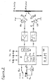
- a security system comprises a microprocessor-based authenticating equipment as shown schematically in Figure 3 .
- the authenticating device comprises a microcontroller or processor 1, embodied for example by the ADuC812 MicroConverterTM of Analog Devices.
- the ADuC812 chip comprises a 16 MHz 8052 microprocessor (CPU) 1a with 32 digital I/O lines, a 5 ⁇ s 12 bit analog/digital (A/D) converter 1b, as well as D/A converters, integrated RAM (256 bytes) and EE/Flash memory (Mem) or memory device 1c for program (8K) and data (640 bytes) storage.
- EE/Flash memory (Mem) 1c is electrically erasable permanent memory and allows for the implementation of a "learning mode".
- the ADuC812 chip's internal memory was complemented in our example with 32 K of external random access memory (RAM) or memory device 1d.
- the authenticating device further contains a laser current driver 2 controlled by the ADuC812, a 980nm wavelength pulse laser diode (LD) as excitation source 3 with collimator optics 3a, as well as a photodetecting chain based on a green-sensitive commercial GaAsP photodiode (PD) 4, an optional optical filter 4a, and a corresponding amplifier 5.
- the photodetecting chain 4,5 is laid out such as to guarantee a minimum bandwidth of 200 kHz, corresponding to the ADuC812's 5 ⁇ s sampling rate; its output is connected to the ADuC812's A/D converter 1b.
- the ADuC812 is further connected to a mode switch SLT for the selection of learning/testing mode L/T, to a push-button B for initiating the measurement cycle, as well as to yellow, green and red LEDs 8a, 8b, 8c for indicating the On/off and the approved/failure (Yes/No) states.
- the push-button B is switching on the circuit's main power supply Vcc.
- a processor-controlled power-hold switch 9 is provided, allowing the processor to hold its own power for completing the measurement cycle and to switch itself off in good conditions.
- a reference decay curve or reference intensity-versus-time emission function is acquired.
- a reference sample 7-R is placed at the position below collimator optics 3a and optical filter 4a.
- the pushbutton B is pressed, powering up the detector unit.
- the laser diode of excitation source 3 is addressed with a short current pulse from the laser current driver 2 (typically 1 A during 200 ⁇ s).
- a 980 nm laser excitation pulse P is focussed by the collimator optics 3a onto a luminescent reference marking M-R of reference sample 7-R.
- the corresponding luminescent response at 550 nm is sensed by the photodiode 4.
- the signal from the photodiode passes into the amplifier 5 and from there into the A/D converter 1b.
- the microprocessor 1 initiates a direct-memory-access (DMA) data acquisition sequence.
- DMA direct-memory-access
- the signal of the photodetecting chain 4,5 is sampled at regular time intervals (for example every 5 ⁇ s) by the A/D converter 1b and stored in subsequent memory locations of the external memory device 1d, Sampling time and number of samples to be taken are preset by the microprocessor's program as a function of the previous results.
- the data in memory device 1d is analyzed, processed, condensed to 64 data points defining reference values VR1 to VR64 ( Fig. 4 ) and stored in the microconverter's permanent memory device 1c.
- the function represented by reference values VR1 - VR64 is furthermore normalized, i.e. the values VR1 - VR6 are scaled with respect to the highest value of the function. Therefore, VR1 - VR64 are independent of overall intensity variations affecting the luminescent emission.
- Figure 4 illustrates the possible form of this reference curve, which is retained as a list of reference values (VR1, VR2, VR3, ...) for the corresponding points in time (t1, t2, t3, ).
- the VRn values may optionally be associated with corresponding individual tolerances ( ⁇ +, ⁇ -).
- a successful termination of the operation is acknowledged by the green "Yes" indicator 8b. Some seconds after termination of the operations, the microprocessor switches off the detector unit via the power supply switch 9.
- a probe decay curve is acquired and compared with the previously stored reference curve.
- a probe sample 7-P comprising a probe marking M-P is placed at the correct sample position.
- the trigger pushbutton B is pressed, powering up the authenticating device.
- the very same sequence of operations as described for the "learning mode” L is performed, up to the point where the measured luminescence decay data is processed and condensed into 64 data points.
- the so obtained data VP1 to VP64 are normalized as well and compared with the previously stored reference values VR1 - VR64.
- the corresponding data points are in our embodiment subtracted from each other, and the absolute values of the differences are summed up for all 64 data points. If the value of this sum is less than a selectable criterion, the test sample is accepted as being "good” and the green "Yes” LED 8b is activated. If the value of said sum exceeds to said criterion, the test sample is refused as being “bad” and the red “No” LED 8c is activated. Some seconds after termination of the operations, the microprocessor switches off the detector unit via power supply switch 9.
- the emission intensity E of a reference sample 7-R or of a sample probe 7-P can vary within a large measure. Aging of the luminescent material or surface alteration of a reference marking M-R or of a probe marking M-P are often the cause. If the marking is, for example, applied to an article 7 such as a banknote or a product tag, the surface of said banknote or the tag may become dirty or scratched. This may substantially reduce the excitation intensity at the luminescent material and may also reduce the intensity of the emission radiation from such a marking. In particular, the emission radiation E of a reference sample 7-R may have higher absolute values than the emission radiation E of a probe sample 7-P.
- the method according to the invention relies on a comparison of decay curve forms, rather than of individual absolute intensity values.
- the number of individual data points VP1 - VPn and VR1 - VRn taken to define probe curve CP and reference curve CR may vary to a high degree. Higher numbers allow generally a more exact definition of a curve.
- this data may be transferred as reference values VR1 - VRn to other authenticating devices.
- each authenticating device may have a number of memory segments to store reference values VR1 - VRn for a number of different markings M.
- reference values VR for comparison may be provided in any way; electronic data may be provided i.e. by internal or external memories, by memory card, by wire- or wireless transmission, as an encrypted memory or data attachment to a sample or in any other suitable way.
- the ADuC812's central processing unit 1a was programmed so as to perform the outlined operations after a pressing of the pushbutton B. They noteworthy comprise the following functional program blocks:
- two excitation light sources 31 and 32 for emitting excitation pulses P of different wavelengths, with collimation optics 31a and 32a and corresponding pulse drivers 21 and 22, are provided.
- the optical elements are arranged such that all optical axes intersect at a single observation point on an probe sample 7-P. Said probe sample 7-P, carrying a probe marking M-P, is conveyed through the authenticating device.
- processor 1 sends a current pulse to light source 31 or to light source 32, or to both of them.
- photodetector 41 and/or of photodetector 42 are examples of photodetector 41 and/or of photodetector 42.
- the device may be laid out for the detection of erbium-based up-converting materials, excited with an excitation source 31 at 980 nm and emitting in the green at 550 nm which will be detected by photodetector 41, simultaneously europium luminescents which are contained in probe marking M-p, are excitated by light source 32 at 370 nm and emitting near 610 nm, which will be detected by photodetector 42. Presence of both luminescent materials is required to confirm authenticating of probe marking M-P.
- the working principles of the device according to this particular embodiment are otherwise the same as those for the first embodiment.
- the device may be designed for the detection of praseodymium based up-converting materials, which must be simultaneously excited with a first laser at 1014 nm and a second laser at 850 nm, and which subsequently emit in the red at about 600 nm ( Figure 7 ).
- excitation pulses P are generated by excitation sources 31 and 32 which are operated simultaneously.
- Pohotodetector 41 is allocated to the monitoring of the 600 nm emission.
- the second photodetector 42 is designed to monitor the 1310 nm praseodymium down-conversion emission, which is present as well.
- even more excitation light sources and/or photodetectors may be incorporated.
- an authenticating device schematically depicted in Figure 6 , a combination of a multiple LED or LD excitation source 3, a focussing grating type micro-spectrometer 4a' comprising a light-guide nozzle, a two-dimensional CCD array 4b' as a photodetector / acquisition device, and a processor 1 to control the acquisition, storage and evaluation of the data, is employed.
- the excitation source 3 preferably comprises a series of light emitting diodes 31, 32, 33, ..., 3n, having emission wavelengths chosen such as to cover the UV, visible and the near infrared part of the light spectrum.
- a set of commercially available LEDs emitting at 370nm (UV), 470nm (blue), 525nm (turquoise), 570nm (green), 590nm (yellow), 610nm (orange), 660nm (red), 700nm (dark red), 740 nm (IR), 770nm (IR), 810nm (IR), 870nm (IR), 905nm (IR) and 950nm (IR) has proven to be useful.
- These LEDs may be disposed at the user's convenience, but are preferably arranged in a circle around the micro-spectrometer's light-guide nozzle.
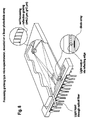
- the focussing grating type micro-spectrometer 4a' is a device according to Figure 8 .
- Light from the probe is coupled into the focal plane of the spectrometer by an optical fiber or light-guide nozzle which acts as a point-shaped light source, illuminating a self-focussing reflection grating.
- This latter focuses the light back onto a linear photodetector array, dispersing the different wavelength components comprised in said light onto adjacent pixels of said array.
- a spectrum of the light from the probe is thus obtained by reading out the pixels of the photodetector array.
- CCD array 4b' For the rapid acquisition of time-dependent spectral information, a two-dimensional charge coupled device (CCD) array 4b' is used.
- CCD arrays comprise a two-dimensional field of photosensitive pixels, which can be read out through a shifting process according to Figure 9a : Pixels are first shifted "vertically", line by line, into a horizontal register. There, the individual pixels are shifted "horizontally", pixel by pixel, to a preamplifier and further to the output.
- Two-dimensional CCD arrays are normally used in video cameras and may comprise between 256 and 1K pixels in each dimension.
- a first line of photosensitive pixels (PIX) of said two-dimensional CCD array serves as the linear photodetector array of said micro-spectrometer device 4a'.
- the remaining lines of CCD pixels are not used as photosensors, but are protected from light influence and play the role of a primary storage device for the time-dependent spectral information.
- the processor 1 controls the data acquisition and treatment process, performing the steps of:
- the achievable time resolution is determined by the line-shifting frequency of step b). This latter can be as high as 4 MHz, corresponding to a time step of 250 ns.
- the read-out of the accumulated data of step c) may occur much more slowly, in a way known to the skilled in the art.
- the available data after step c) corresponds to a "picture frame", having a spectral dimension and a time dimension.
- a time-decay curve can be obtained from this frame by slicing out a time-fringe at the appropriate wavelength; this information can be treated and evaluated as given in the one-dimensional examples above.
- the analysis can, alternatively, be extended to more than one wavelength, or also combined with spectral analysis, taking profit of the second dimension of the acquired data frame.
Abstract
Description
- The invention is in the field of security markings, applied through inks or coating compositions or in bulk materials, and of documents or articles carrying such security markings. It concerns a novel method for exploiting the characteristics of certain luminescent pigments incorporated into said inks, coating compositions or articles. In particular, it deals with a method and a device allowing to exploit the characteristic luminescent afterglow of certain luminescent materials and luminescent compounds and proposes a security system for marking and authenticating an item.
- Luminescent materials are among the classic ingredients of security inks or coatings. They convert energy of an exciting radiation of a given wavelength into emitted light of another wavelength. The exploited luminescent emission can lie in the UV range (below 400 nm), in the visible range (400 - 700 nm) or in the near to mid infrared range (700-2500 nm) of the electromagnetic spectrum. Certain luminescent materials can emit simultaneously at more than one wavelength. Most luminescent materials can be excited at more than one wavelength.
- If the emitted radiation has a longer wavelength than the exciting radiation, one speaks of "Stokes" or "down-converting" luminescence. If the emitted radiation has a shorter wavelength than the exciting radiation, one speaks of "anti-Stokes" or "up-converting" luminescence.
- Luminescence can be of two different types: fluorescence or phosphorescence. Fluorescence is the prompt emission of radiation upon excitation, whereas phosphorescence is the time-delayed emission of radiation, observable after the excitation has been stopped. Phosphorescence, also called afterglow, is characterized by a specific decay of the luminescence intensity in function of time; the corresponding lifetimes, which are material-specific, can range from the nanosecond to the multi-hour time scale.
- Luminescent materials can be of organic or of inorganic nature. Examples of the former are the cyanine type molecules, as well as the coumarines, rhodamines etc. Examples of the latter are the copper or silver doped zinc sulfides, the rare-earth doped yttrium aluminum garnets or yttrium vanadates, etc. Another class of luminescents can be found among the metallo-organic compounds, e.g. the silicon phthalocyanines, the rare-earth beta-diketonates etc.
- Luminescent materials can be employed in inks or coatings either as pigments or as soluble materials. Newer developments have also made available luminescent pigments in colloidal form. Particular applications rely as well on luminescent polymers, obtained by polymerizing, copolymerising or grafting luminescent molecules into or onto a polymer chain.
- All of these compound classes and application forms have been used in security compositions and for security purposes. Corresponding detecting equipment can be made to discriminate between prompt luminescence (fluorescence) or delayed luminescence (phosphorescence).
-
US 3,473,027 deals with the general use of organic and inorganic rare-earth compounds as visible and IR luminescent markers for applications such as goods identification and labels, personal identification, identification and registration of passing vehicles, machine reading of information, ZIP codes, invoices, tags etc. and high capacity storage devices. The patent further describes a "spectroscopic detector" for discriminating between different narrow-line luminescent responses. -
US 3,412,245 adds the decay-time characteristics of the luminescence to the encoding factors. In this way, rare-earth based luminescents, having decay times of the order of milliseconds, can be distinguished from much more rapidly decaying organic fluorescent material. The discrimination is done via excitation with sinusoidally modulated or pulsed UV light sources, using variable modulation or pulse frequency, in conjunction with spectral separation of the different emission wavelengths. -
US 3,582,623 andUS 3,663,813 reveal further developments of spectroscopic detecting equipment for luminescent features. -
US 3,650,400 describes the use of a pulsating light source, in conjunction with synchronous detection at the pulsating frequency ("lock-in" principle), to suppress the influence of ambient light. By this means, the detector is only sensitive to the luminescent's proper response. The principal shortcoming of methods of the prior art, which rely on a determination of the material's modulation-transfer function, is their inherent slowness. For these reason they are not normally implemented on high-speed authenticating machines. -
US 4,047,033 describes the use of an up-converting luminescent material for security purposes, as well as corresponding detecting equipment. Detection relies on excitation with a GaAs IR-LED, emitting at 950 nm wavelength in continuous or pulsed mode, combined with spectroscopic identification of the luminescent emission. Reference is made to indirect means, by measuring pulse dephasing, for assessing the characteristic rise and decay times of the luminescent's response. This method is, however, strongly affected by variations in luminescence intensity, and therefore not easy to implement in practice. - Another method of the prior art, suited for high-speed authentication, relies on pulse-excitation of a moving test sample on a conveyor belt. After passing the UV excitation source, the intensity of the induced luminescence decays according to the intrinsic decay characteristics of the material. One or several photodetectors, placed at determined distances from the UV source along the conveyor belt, are used to assess specific points of said decay characteristics. The main drawback of this method is its limitation to such phosphorescent materials which have characteristic luminescence decay times of the order of 50 milliseconds. This limitation is a consequence of the mechanical constraints (conveyor belt speed) of the detecting process.
- It is an object of the present invention to provide a method, a device and a security system which overcome the shortcomings of the prior art. In particular, the invention shall permit a rapid sampling of a luminescence decay characteristic and shall be, therefore, suitable for high-speed machine reading applications.
- Furthermore, the invention shall allow a wide choice of up- or down-converting phosphorescent materials, having decay times from the sub-microseconds to the ten milliseconds range or longer. A further particular object of the invention is to render the authentication process more reliable by compensating for alterations of luminescence intensity, which may occur due to changes in the luminecent marking itself (ageing, dirtiness) or in the measuring equipment.
- The above objects are primarily achieved by a method, a device and a security system for authenticating a luminescent probe marking and according to the independent claims. The invention is based on a comparison of the time-dependent luminescence emission functions of a probe material with that of a reference material. Therefore, according to the invention, curve shapes are used as the authenticating feature, rather than intensity values of individual measurements. Said emission functions are compared in normalized form. In doing so, the comparison becomes largely independent of intensity deviations due to aging, alterations or dirtiness.
- The invention relies further on the direct assessment of the time-dependent luminescence emission function of a probe marking following pulse excitation. The luminescence may hereby be excited using any kind of intense, pulsed radiation source, for example light emitting diodes, laser diodes, Q-switched lasers and light sources derived thereof by nonlinear optics, as well as X-ray pulses or particle beams, in particular pulsed electron beams. After excitation with an appropriate excitation pulse, preferably with a light pulse of appropriate wavelength and duration, the luminescent material emits part of the absorbed energy in the form of emission radiation of a second wavelength. In some cases, said emission of radiation occurs almost immediately, and stops with the excitation stopping. In other cases, the emission is time-delayed and the intensity of the emitted radiation follows either a simple exponential decay law, or more complicated laws of hyperbolic shape, or even shows a rise and decay behavior, representative of complicated internal energy transfer processes and of competing decay mechanisms. In every case, however, the observed evolution of the emission intensity as a function of time, after the ceasing of the external stimulation, depends only on the luminescent material itself, and serves thus as an authenticating feature, indicating the presence of said specific material. Even if the absolute luminescence intensity is reduced, e.g. by aging or dirtiness of the material, the shape of the emission-versus-time function is preserved, as it is typical for a luminescent compound.
- In the context of this invention, decay or decay-curve shall mean any specific intensity-versus-time function of a probe and its reference. Such an intensity-versus-time function represents the measured response of the luminescence emission intensity due to an excitation pulse. The term excitation source" shall furthermore apply to electromagnetic sources of radiation having a wavelength comprised in between 200 nm and 2'500 nm, including thus UV light, visible light, and short-wavelength (non-thermal) IR light. Alternative methods of stimulation, using e.g. X-ray or electron-beam pulses are possible and included by said definition as well.
- In performing the method and using the authenticating device the emission intensity of a probe is sampled at appropriate time intervals and stored in an analog memory, e.g. digitized by an analog-to-digital (AD) converter and stored in a digital memory.
- A reference curve of the luminescent's emission as a function of time, taken on a reference sample by using the same instrumental set-up and procedure, is stored in a digital memory, too, and provided for comparison and authentication.
- Authentication of a probe under test is performed by a point-by-point comparison of its luminescence decay curve with the stored reference sample's decay curve.
- Probe and reference emission functions are compared in normalized form. Normalization implies that the intensity values of both emission functions are put to scale, such that the highest values of both decay curves coincide.
- If said comparison of the probe decay curve with the corresponding reference decay curve confirms identity within definable tolerances, a conformity signal is provided to authenticate the probe. In the opposite case, non-conformity is assumed. The conformity- or non-conformity-signal may be any electric, optical, acoustic or other signal.
- Said definable tolerance may be conceived on a point-by-point base, i.e. each probe curve point is compared with its corresponding reference curve point and must lie within absolute (e.g. + 50 / - 30), relative (e.g. ± 20%) or individually defined limits from that reference curve point. On the point-by-point base, all points must lie inside their respective tolerances for the probe sample to be accepted.
- Alternatively, an overall tolerance criterion may be applied; i.e. the individual differences of corresponding probe and reference intensities, or some convenient function thereof like the squares or the absolute values, etc., are summed up over all points, and the resulting sum is checked against said overall tolerance criterion.
- The method of the invention has the advantage of being applicable to any type of luminescence decay characteristics, be it exponential or not. It is in particular applicable to the authentication of mixtures of luminescents having a same particular luminescent center in environments with different decay characteristics. E.g. a mixture of YVO4:Eu and Y2O2S:Eu can be distinguished in this way from its single components.
- The method according to the invention can be laid out such that a "single shot" measurement i.e. a single excitation light pulse followed by the acquisition of the corresponding luminescence response as a function of time, lasting in the order of a millisecond, is sufficient to collect the complete luminescence decay information of a probe and to compare it with the reference data. Hence, high speed operation on fast moving samples is herewith assured.
- However, in the case of a weak luminescence, i.e. of an insufficient signal-to-noise (S/N) ratio, the measurement can also be repeated a certain number of times and the results of more than one of said "shots" can be averaged together on a point by point base to improve the S/N ratio and hence to obtain the desired decay curve information with a higher statistical precision.
- It is a further advantage of the method of the present invention that it is model-free, i.e. that the luminescence decay curve itself is used as the authenticating feature, rather than a parameter derived thereof. Derivation of parameters is always tied to a physical model and becomes inapplicable in case the model does not hold. Model-free methods have therefore a far larger application range than model-tied ones.
- The method according to the invention can be used in conjunction with other existing techniques for the spectral identification of luminescent responses. In particular, it can be used in conjunction with spectral filters, wavelength-dispersive elements, optical gratings or other optical instrumentation which lead to a wavelength selection.
- Light collection optics can be used as well, in order to improve the signal-to-noise ratio of the photodetecting chain.
- More than one detection channel can be provided for the simultaneous detection of luminescent mixtures, or of luminescents emitting at more than one wavelength simultaneously. The latter is often the case in rare-earth ion based luminescent materials. The different detection channels are hereby provided with appropriate wavelength selectors, and the corresponding intensity-versus-time data are individually sampled and stored.
- In a particular embodiment, the detection channel is a micro-spectrometer unit, comprising a wavelength-dispersor (e.g. a prism, a grating, or a linearly variable filter) and an array-photodetector. The latter can be a linear photodiode array or a linear CCD (charge coupled device) array. To assure high operation speed, a modified two-dimensional CCD matrix array can be employed in place of the linear CCD array.
- In CCD matrix arrays, an image frame of photogenerated charge carriers, produced by the exposure of the silicon chip to light, is "vertically" shifted, line by line, to the edge of the chip, where the individual lines are then "horizontally" shifted and read out, pixel by pixel. These shifting processes are taking place in parallel, and huge amounts of data can be handled very rapidly (typical speeds for a 256 x 256 CCD array are up to 40 MHz for "horizontal" pixel-to-pixel shifting, and up to 4 MHz for "vertical" line-to-line shifting).
- Said modified CCD matrix array is laid out such that a first line of pixels is acting as the photodetector array for the spectrum produced by said wavelength-dispersor. The subsequent lines of pixels are protected from the influence of light and serve as an intermediate mass storage device. Following the excitation pulse, the time-dependent spectral information is acquired by a rapid "vertical" line-to-line shifting and stored in the CCD's light-protected area for subsequent read out by the instrument's processor.
- More than one excitation source can be provided, in order to gain hardware flexibility for detecting luminescents having different excitation wavelengths. Light emitting diodes (LEDs) in particular are well suited for the illumination of a spectral range of about 50 nm bandwidth. Providing a set of different LEDs allows to cover a larger spectral area of interest. This multi-LED light source can be controlled by the instruments microprocessor, such that the choice of the excitation wavelength can be performed by mere programming.
- It is of particular interest to combine said multi-LED light source with said microspectrometric detector unit, to obtain an universal luminescence / decay time detector module.
- According to the invention, the very same equipment can be used to define the reference decay curve and to authenticate an unknown sample. The equipment can thus be operated in a "learning mode", where a reference decay curve (reference intensity-versus-time emission function) is acquired from a reference sample, appropriately processed and the corresponding data stored in a memory. The equipment can also be operated in a "testing mode", where a luminescence decay curve of a probe (probe intensity-versus-time emission function), carrying a marking to be authenticated, is acquired, the corresponding data appropriately processed and compared with the previously stored reference data, in order to derive a conformity / non-conformity indicator. The same device would thus be operated in a "learning mode" to store reference data in the memory, and later on for testing probes in a "testing mode". The device may also comprise more than one memory segment to provide reference data for the authentication of different markings.
- Said "learning mode" and said "testing mode" need not, however, to be necessarily implemented within the same physical unit or device. In an alternative embodiment, a first device is dedicated to the acquisition / definition of a reference decay curve from the reference sample. The reference data are then transferred to the memory of a second, similar, device, which is exclusively dedicated to the authentication of probe samples.
- The method and equipment according to the invention can be used to authenticate inks and/or coating compositions comprising suitable luminescent material, as well as articles such as security articles or coated articles realized using said inks and/or coating compositions.
- Said method and equipment can furthermore be used to authenticate suitable luminescent bulk material, such as paper or plastic used for the manufacturing of articles such as bank notes, security documents, identity cards, credit cards, security threads, labels and other security articles.
- A security system can be realized based on the outlined method by providing a set of reference samples comprising luminescent materials and/or luminescent compounds of similar spectral emission (i.e. emission color), but having different time-dependent emission functions. Said reference samples are distinguishable by the method and the device according to the invention, e.g. by incorporating one or more of them into a marking on an item, for authentication purposes.
- The invention is further exemplified by the embodiments of security systems and of authenticating devices as described below and as shown in the following drawings:
- Fig. 1
- shows the emission spectrum of an up-converting phosphor which can be used in connection with the invention,
- Fig. 2
- shows luminescence decay curves of four different up-converting luminescent phosphors, which can be used to constitute a security system according to the invention
- Fig. 3
- shows the block diagram of a first embodiment of an authenticating device in accordance with the invention,
- Fig. 4
- shows a typical luminescence intensity / time characteristics, which can be used for authenticating purposes in accordance with the present invention,
- Fig. 5
- shows a schematic block diagram for a modified embodiment of a detecting device according to the invention,
- Fig. 6
- shows a schematic view of a more sophisticated embodiment of a detecting device according to the invention,
- Fig. 7
- shows the energy levels of the prasodymium(3+) ion,
- Fig. 8
- shows a focussing grating type micro-spectrometer, mounted on a linear photodiode array,
- Fig. 9a
- shows the principle of read-out of a two-dimensional CCD array,
- Fig. 9b
- shows the principle of data shifting in a CCD array.
- A security system according to the invention comprises a microprocessor-based authenticating equipment as shown schematically in
Figure 3 . - As representatives of the collection of luminescent compounds in a marking, four erbium-based up-converting phosphors of different nature were chosen to: Gd2O2S:Er,Yb; Y2O2S:Er,Yb; BaY2F8:Er,Yb; NaYF4:Er,Yb. Upon irradiation with a 950 or 980 nm light source, all of them emit in the green, near 550 nm (
Figure 1 ). The lifetimes of the green, phosphorescent emissions are, however, very different for the four materials, as shown inFigure 2 . - The authenticating device, as shown in
Figure 3 , comprises a microcontroller orprocessor 1, embodied for example by the ADuC812 MicroConverter™ of Analog Devices. The ADuC812 chip comprises a 16 MHz 8052 microprocessor (CPU) 1a with 32 digital I/O lines, a 5µs 12 bit analog/digital (A/D) converter 1b, as well as D/A converters, integrated RAM (256 bytes) and EE/Flash memory (Mem) or memory device 1c for program (8K) and data (640 bytes) storage. EE/Flash memory (Mem) 1c is electrically erasable permanent memory and allows for the implementation of a "learning mode". The ADuC812 chip's internal memory was complemented in our example with 32 K of external random access memory (RAM) ormemory device 1d. - The authenticating device further contains a laser
current driver 2 controlled by the ADuC812, a 980nm wavelength pulse laser diode (LD) asexcitation source 3 with collimator optics 3a, as well as a photodetecting chain based on a green-sensitive commercial GaAsP photodiode (PD) 4, an optional optical filter 4a, and acorresponding amplifier 5. Thephotodetecting chain - In the "learning mode" L, a reference decay curve or reference intensity-versus-time emission function is acquired. A reference sample 7-R is placed at the position below collimator optics 3a and optical filter 4a. After setting the SLT switch to "learning mode" L, the pushbutton B is pressed, powering up the detector unit. Controlled by the
microprocessor 1, the laser diode ofexcitation source 3 is addressed with a short current pulse from the laser current driver 2 (typically 1 A during 200 µs). A 980 nm laser excitation pulse P is focussed by the collimator optics 3a onto a luminescent reference marking M-R of reference sample 7-R. The corresponding luminescent response at 550 nm (emission radiation E) is sensed by thephotodiode 4. The signal from the photodiode passes into theamplifier 5 and from there into the A/D converter 1b. After pulsing the laser diode, themicroprocessor 1 initiates a direct-memory-access (DMA) data acquisition sequence. During this sequence, the signal of thephotodetecting chain external memory device 1d, Sampling time and number of samples to be taken are preset by the microprocessor's program as a function of the previous results. After termination of the sampling, the data inmemory device 1d is analyzed, processed, condensed to 64 data points defining reference values VR1 to VR64 (Fig. 4 ) and stored in the microconverter's permanent memory device 1c. The function represented by reference values VR1 - VR64 is furthermore normalized, i.e. the values VR1 - VR6 are scaled with respect to the highest value of the function. Therefore, VR1 - VR64 are independent of overall intensity variations affecting the luminescent emission.Figure 4 illustrates the possible form of this reference curve, which is retained as a list of reference values (VR1, VR2, VR3, ...) for the corresponding points in time (t1, t2, t3, ...). The VRn values may optionally be associated with corresponding individual tolerances (Δ+, Δ-). - A successful termination of the operation is acknowledged by the green "Yes" indicator 8b. Some seconds after termination of the operations, the microprocessor switches off the detector unit via the power supply switch 9.
- In the "testing mode" T a probe decay curve is acquired and compared with the previously stored reference curve. According to
Fig. 3 a probe sample 7-P comprising a probe marking M-P is placed at the correct sample position. After setting the SLT switch to "testing mode" T, the trigger pushbutton B is pressed, powering up the authenticating device. The very same sequence of operations as described for the "learning mode" L is performed, up to the point where the measured luminescence decay data is processed and condensed into 64 data points. The so obtained data VP1 to VP64 are normalized as well and compared with the previously stored reference values VR1 - VR64. To compare the data representing the decay curve of a probe marking M-P with that of a reference marking M-R, the corresponding data points are in our embodiment subtracted from each other, and the absolute values of the differences are summed up for all 64 data points. If the value of this sum is less than a selectable criterion, the test sample is accepted as being "good" and the green "Yes" LED 8b is activated. If the value of said sum exceeds to said criterion, the test sample is refused as being "bad" and the red "No" LED 8c is activated. Some seconds after termination of the operations, the microprocessor switches off the detector unit via power supply switch 9. - The emission intensity E of a reference sample 7-R or of a sample probe 7-P can vary within a large measure. Aging of the luminescent material or surface alteration of a reference marking M-R or of a probe marking M-P are often the cause. If the marking is, for example, applied to an
article 7 such as a banknote or a product tag, the surface of said banknote or the tag may become dirty or scratched. This may substantially reduce the excitation intensity at the luminescent material and may also reduce the intensity of the emission radiation from such a marking. In particular, the emission radiation E of a reference sample 7-R may have higher absolute values than the emission radiation E of a probe sample 7-P. - Therefore, the method according to the invention relies on a comparison of decay curve forms, rather than of individual absolute intensity values.
- After normalizing both curves with respect to their highest value between t1 and tn, two identical curves are obtained for samples containing the same luminescent, even if the latter is present in different concentration. By applying this general principle of comparing normalized curves, the authentication process will not be affected by factors resulting in intensity or measurement deviations.
- The number of individual data points VP1 - VPn and VR1 - VRn taken to define probe curve CP and reference curve CR may vary to a high degree. Higher numbers allow generally a more exact definition of a curve.
- For practical purposes, a number between 32 and 128 values, preferably 64 values, has proven to be sufficient.
- After deriving reference values VR1 - VRn in
RAM 1d or in permanent memory device 1c, this data may be transferred as reference values VR1 - VRn to other authenticating devices. - Similarly, each authenticating device may have a number of memory segments to store reference values VR1 - VRn for a number of different markings M. Generally, reference values VR for comparison may be provided in any way; electronic data may be provided i.e. by internal or external memories, by memory card, by wire- or wireless transmission, as an encrypted memory or data attachment to a sample or in any other suitable way.
- The ADuC812's central processing unit 1a was programmed so as to perform the outlined operations after a pressing of the pushbutton B. They noteworthy comprise the following functional program blocks:
- assure autonomy of power supply during the measurement cycle by setting switch 9 on,
- read learning/testing mode switch SLT,
- if learning mode L:
- prepare the external memory for DMA data acquisition,
- pulse the laser diode,
- acquire a predetermined number of samples of the luminescent's response in DMA mode into
memory device 1d, - post-process the sampled data and compress it in an optimized form into 64 data points,
- store the compressed and normalized data, including a compression indicator, in the ADuC812's internal permanent data EE/Flash memory device 1c, as a reference.
- if testing mode T:
- prepare the external memory for DMA data acquisition,
- pulse the laser diode,
- acquire a predetermined number of samples of the luminescent's response in DMA mode into
memory device 1d, - post-process the sampled data and compress it into 64 normalized data points according to the previously stored compression indicator,
- compare the compressed and normalized data with the previously stored normalized reference data in memory device 1c, and derive a conformity / non-conformity indicator,
- set the approved/failure indicator LEDs correspondingly, to show the result.
- after a waiting period of predetermined length, switch off the power supply via switch 9.
- In a modified embodiment of an authenticating device according to the invention, schematically shown in
Figure 5 , twoexcitation light sources amplifiers 51 and 52, are provided, too. The optical elements are arranged such that all optical axes intersect at a single observation point on an probe sample 7-P. Said probe sample 7-P, carrying a probe marking M-P, is conveyed through the authenticating device. Depending on the feature to be detected,processor 1 sends a current pulse tolight source 31 or to lightsource 32, or to both of them. Depending on the emission to be detected, use is made of photodetector 41 and/or of photodetector 42. - As example, the device may be laid out for the detection of erbium-based up-converting materials, excited with an
excitation source 31 at 980 nm and emitting in the green at 550 nm which will be detected by photodetector 41, simultaneously europium luminescents which are contained in probe marking M-p, are excitated bylight source 32 at 370 nm and emitting near 610 nm, which will be detected by photodetector 42. Presence of both luminescent materials is required to confirm authenticating of probe marking M-P. The working principles of the device according to this particular embodiment are otherwise the same as those for the first embodiment. - In another particular embodiment, the device may be designed for the detection of praseodymium based up-converting materials, which must be simultaneously excited with a first laser at 1014 nm and a second laser at 850 nm, and which subsequently emit in the red at about 600 nm (
Figure 7 ). In the embodiment, excitation pulses P are generated byexcitation sources - In still another, more sophisticated embodiment of an authenticating device according to the invention, schematically depicted in
Figure 6 , a combination of a multiple LED orLD excitation source 3, a focussing grating type micro-spectrometer 4a' comprising a light-guide nozzle, a two-dimensional CCD array 4b' as a photodetector / acquisition device, and aprocessor 1 to control the acquisition, storage and evaluation of the data, is employed. - The
excitation source 3 preferably comprises a series oflight emitting diodes - The focussing grating type micro-spectrometer 4a' is a device according to
Figure 8 . Light from the probe is coupled into the focal plane of the spectrometer by an optical fiber or light-guide nozzle which acts as a point-shaped light source, illuminating a self-focussing reflection grating. This latter focuses the light back onto a linear photodetector array, dispersing the different wavelength components comprised in said light onto adjacent pixels of said array. A spectrum of the light from the probe is thus obtained by reading out the pixels of the photodetector array. - For the rapid acquisition of time-dependent spectral information, a two-dimensional charge coupled device (CCD) array 4b' is used. Such CCD arrays comprise a two-dimensional field of photosensitive pixels, which can be read out through a shifting process according to
Figure 9a : Pixels are first shifted "vertically", line by line, into a horizontal register. There, the individual pixels are shifted "horizontally", pixel by pixel, to a preamplifier and further to the output. Two-dimensional CCD arrays are normally used in video cameras and may comprise between 256 and 1K pixels in each dimension. The shifting of pixel information, present as stored photo-generated electrons, is explained inFigure 9b : Three electrodes (1, 2, 3) are present for each pixel, which are driven with triphase positive clock signals (φ1, φ2, φ3). The electrons always accumulate in positive potential wells, represented by a "down" state. The up and down phases of the clock signals are made to overlap such as to result in a shift of the stored electrons of the whole array by one pixel after a clock period (t1 to t6), i.e.:t1 t2 t3 t4 t5 t6 φ1: up up up down down down φ2: down down up up up down φ3: up down down down up up - In the context of the invention, a first line of photosensitive pixels (PIX) of said two-dimensional CCD array serves as the linear photodetector array of said micro-spectrometer device 4a'. The remaining lines of CCD pixels are not used as photosensors, but are protected from light influence and play the role of a primary storage device for the time-dependent spectral information.
- The
processor 1 with its memory device 1c controls the data acquisition and treatment process, performing the steps of: - pulsing the appropriate diode or diodes of
excitation source 3, in order to excite the luminescence marking of probe sample 7-P respectively reference sample 7-R, following the light pulse, performing an appropriate number of line-shiftings in the CCD array, in order to record the time-dependent spectral response information as a two-dimensional picture frame in the protected area of said array, reading out the time-dependent spectral response information from the CCD array and storing it in the memory device 1c, post-treating and evaluating the collected time-dependent spectral information in terms of the authentication task to be performed. - The achievable time resolution is determined by the line-shifting frequency of step b). This latter can be as high as 4 MHz, corresponding to a time step of 250 ns. The read-out of the accumulated data of step c) may occur much more slowly, in a way known to the skilled in the art. The available data after step c) corresponds to a "picture frame", having a spectral dimension and a time dimension. A time-decay curve can be obtained from this frame by slicing out a time-fringe at the appropriate wavelength; this information can be treated and evaluated as given in the one-dimensional examples above. The analysis can, alternatively, be extended to more than one wavelength, or also combined with spectral analysis, taking profit of the second dimension of the acquired data frame.
Claims (17)
- Method for authenticating a luminescent probe marking (M-P), comprising the steps of:- exciting said luminescent probe marking (M-P) with at least one excitation pulse (P) of at least one excitation source (3, 31 - 36),- measuring probe intensity values (VP1 - VPn) of emission intensity (I) from emission radiation (E) of said luminescent probe marking (M-P) in response to said at least one excitation pulse (P) at time intervals (t1 - tn),- forming a probe intensity-versus-time emission function of said probe intensity values (VP1 - VPn),- comparing said probe intensity-versus-time emission function with at least one reference intensity-versus-time emission function,- said probe intensity-versus-time emission function and said reference intensity-versus-time emission function are normalized prior to comparison.
- Method according to claim 1, characterized in that at least one luminescent probe marking (M-P) is part of a probe sample (7-P) to be authenticated and that specific emission characteristics of said at least one luminescent probe marking (M-P) are measured, said specific emission characteristics include at least one excitation wavelength of said excitation pulse (P), at least one emission wavelength of said emission radiation (E) and probe intensity values (VP1 - VPn) of emission intensity (I) at time intervals (t1 - tn) for at least one of said emission wavelength.
- Method according to claim 1 or 2, characterized in that at least one luminescent reference marking (M-R) is part of a reference sample (7-R) and that specific emission characteristics of said at least one luminescent reference marking (M-R) are measured, said specific emission characteristics include at least one excitation wavelength of said excitation pulse (P), at least one emission wavelength of said emission radiation (E) and reference intensity values (VR1-VRn) of emission intensity (I) at time intervals (t1 - tn) for at least one of said emission wavelength.
- Method according to claim 3, characterized in that reference intensity values (VR1 - VRn) and/or at least one reference intensity-versus-time emission function is/are stored in at least one memory device (1c, 1d).
- Method according to claim 4, characterized in that said at least one reference intensity-versus-time emission function is stored in a normalized form and/or in a non-normalized form.
- Method according to one of the preceding claims, characterized in that said luminescent probe marking (M-P) respectively reference marking (M-R) is excited with at least one excitation pulse (P) from at least one excitation source (3, 31 - 36) being a laser and/or a light emitting diode.
- Method according to one of the preceding claims, characterized in that said luminescent probe marking (M-P) respectively reference marking (M-R) is excited with at least one excitation pulse (P) of electrons.
- Device for authenticating a luminescent probe marking (M-P), comprising:- at least one detector (4, 41, 42, 4b) for measuring probe intensity values (VP1 - VPn) of emission intensity (I) from emission radiation (E) of said luminescent probe marking (M-P) in response to at least one excitation pulse (P) generated by at least one excitation source (3, 31 - 36) at time intervals (t1 - tn),- at least one processor (1) for forming probe intensity-versus-time emission function of said probe intensity values (VP1 - VPn),- at least one processor (1) for comparing said probe intensity-versus-time emission function with at least one reference intensity-versus-time emission function and- at least one processor (1) for normalizing said probe intensity-versus-time emission function prior to comparison with a normalized reference probe intensity-versus-time emission function.
- Device according to claim 8, characterized in that it comprises at least one memory device (1c, 1d) for storing reference intensity values (VR1 - VRn) of emission intensity (I) at time intervals (t1 - tn) for at least one wavelength of emission radiation (E) of said luminescence reference marking (M-R) and/or for storing at least one reference intensity-versus-time emission function formed from reference intensity values (VR1 - VRn) .
- Device according to one of claims 8 to 9, characterized in that it comprises said at least one excitation source (3, 31 - 36).
- Device according to one of claims 8 to 10, characterized in that said at least one detector (4) comprises a wavelength selector (4a').
- Device according to one of claims 8 to 11, characterized in that said at least one detector (4, 41, 4b) converts emission intensity (I) into electric signals of probe intensity values (VP1 - VPn) respectively of reference intensity values (VR1 - VRn) and that said at least one processor (1) samples said electric signals to form a probe intensity-versus-time emission function of said probe intensity values (VP1 - VPn) respectively to form a reference intensity-versus-time of reference emission function of said reference intensity values (VR1 - VRn).
- Device according to one of claims 8 to 12, characterized in that it comprises at least one spectrometer for differentiating between two or more emission wavelengths and that said at least one detector (4b) is an array-photodetector for measuring the emission radiation (E) at two or more emission wavelengths, allowing a simultaneous measuring of probe intensity values (VP1 - VPn) of emission radiation (E) of a luminescent probe marking (M-P) respectively a simultaneous measuring of reference intensity values (VR1 - VRn) of emission radiation (E) of a luminescent reference marking (M-R).
- Device according to claim 13, characterized in that said at least one array-photodetector (4b) is a two-dimensional CCD array, a first row of photosensitive pixels (PIX) works as as photodetecting array, the remaining rows of pixels work as a primary storage device for spectral information as a function of time through a line-shifting process.
- Security system for authenticating a luminescent probe marking (M-P), comprising:- a device according to one of claims 8 to 14,- at least one reference sample (7-R) comprising at least one luminescent reference marking (M-R) for measuring reference intensity values (VR1 - VRn) of emission intensity (I) at time intervals (t1 - tn) for at least one wavelength of the emission radiation (E) of said luminescent reference marking (M-R) and- at least one probe sample (7-P) comprising at least one luminescent probe marking (M-P) for measuring probe intensity values (VP1 - VPn) of emission intensity (I) at time intervals (t1 - tn) for at least one wavelength of the emission radiation (E) of said luminescent probe marking (M-P).
- Security system according to claim 15, characterized in that at least one of said probe sample (7-P) is part of an ink and/or coating composition of an article (7) to be authenticated.
- Security system according to claim 15, characterized in that at least one of said probe samples (7-P) is contained in a bulk material of an article (7) to be authenticated.
Priority Applications (27)
| Application Number | Priority Date | Filing Date | Title |
|---|---|---|---|
| AT00110404T ATE412224T1 (en) | 2000-05-16 | 2000-05-16 | METHOD, DEVICE AND SYSTEM FOR AUTHENTICATION OF A MARKING |
| DK00110404T DK1158459T3 (en) | 2000-05-16 | 2000-05-16 | Procedure, decor and security system, all to correct a selection |
| EP00110404.1A EP1158459B2 (en) | 2000-05-16 | 2000-05-16 | Method, device and security system, all for authenticating a marking |
| DE60040595T DE60040595D1 (en) | 2000-05-16 | 2000-05-16 | Method, device and system for authenticating a marker |
| ES00110404.1T ES2312314T5 (en) | 2000-05-16 | 2000-05-16 | Method, device and security system, all to authenticate a dial |
| PT00110404T PT1158459E (en) | 2000-05-16 | 2000-05-16 | Method, device and security system, all for authenticating a marking |
| PL358198A PL220373B1 (en) | 2000-05-16 | 2001-04-28 | Method, device and security system, all for authenticating a marking |
| CNB018095356A CN1258740C (en) | 2000-05-16 | 2001-04-28 | Method, device and security system for authenticating marking |
| NZ521960A NZ521960A (en) | 2000-05-16 | 2001-04-28 | Method, device and security system, all for authenticating a marking |
| UA2002129868A UA72628C2 (en) | 2000-05-16 | 2001-04-28 | Method, device and security system for authenticating marking |
| AU6590901A AU6590901A (en) | 2000-05-16 | 2001-04-28 | Method, device and security system, all for authenticating a marking |
| HU0301927A HU225867B1 (en) | 2000-05-16 | 2001-04-28 | Method, device and security system for authenticating luminescent a markings |
| TR2002/02533T TR200202533T2 (en) | 2000-05-16 | 2001-04-28 | Method, device and security system for verifying a marking |
| MXPA02011299A MXPA02011299A (en) | 2000-05-16 | 2001-04-28 | Method, device and security system, all for authenticating a marking. |
| PL389383A PL217943B1 (en) | 2000-05-16 | 2001-04-28 | Device and protective system for labelling authentication |
| EA200201203A EA007887B1 (en) | 2000-05-16 | 2001-04-28 | Method, device and security system, all for authenticating a marking |
| AU2001265909A AU2001265909B2 (en) | 2000-05-16 | 2001-04-28 | Method, device and security system, all for authenticating marking |
| JP2001584362A JP5172066B2 (en) | 2000-05-16 | 2001-04-28 | Method, apparatus and security system for authenticating a mark |
| US10/257,983 US7067824B2 (en) | 2000-05-16 | 2001-04-28 | Method, device and security system, all for authenticating a marking |
| CA002408459A CA2408459C (en) | 2000-05-16 | 2001-04-28 | Method, device and security system, all for authenticating a marking |
| CZ20023762A CZ299020B6 (en) | 2000-05-16 | 2001-04-28 | Method, device and security system for authenticating a marking |
| KR1020027013816A KR100795763B1 (en) | 2000-05-16 | 2001-04-28 | Method, device and security system, all for authenticating a marking |
| PCT/EP2001/004809 WO2001088846A1 (en) | 2000-05-16 | 2001-04-28 | Method, device and security system, all for authenticating a marking |
| BRPI0110803-4A BRPI0110803B1 (en) | 2000-05-16 | 2001-04-28 | Method, device and security system, all for authentication of a dial |
| NO20025462A NO335743B1 (en) | 2000-05-16 | 2002-11-14 | Method, device and security system for authentication of a mark |
| ZA200210071A ZA200210071B (en) | 2000-05-16 | 2002-12-12 | Method, device and security system, all for authenticating a marking. |
| HK03108258A HK1056032A1 (en) | 2000-05-16 | 2003-11-13 | Method, device and security system, all for authenticating a marking |
Applications Claiming Priority (1)
| Application Number | Priority Date | Filing Date | Title |
|---|---|---|---|
| EP00110404.1A EP1158459B2 (en) | 2000-05-16 | 2000-05-16 | Method, device and security system, all for authenticating a marking |
Publications (4)
| Publication Number | Publication Date |
|---|---|
| EP1158459A1 EP1158459A1 (en) | 2001-11-28 |
| EP1158459B1 EP1158459B1 (en) | 2008-10-22 |
| EP1158459B9 true EP1158459B9 (en) | 2009-03-25 |
| EP1158459B2 EP1158459B2 (en) | 2017-02-15 |
Family
ID=8168731
Family Applications (1)
| Application Number | Title | Priority Date | Filing Date |
|---|---|---|---|
| EP00110404.1A Expired - Lifetime EP1158459B2 (en) | 2000-05-16 | 2000-05-16 | Method, device and security system, all for authenticating a marking |
Country Status (25)
| Country | Link |
|---|---|
| US (1) | US7067824B2 (en) |
| EP (1) | EP1158459B2 (en) |
| JP (1) | JP5172066B2 (en) |
| KR (1) | KR100795763B1 (en) |
| CN (1) | CN1258740C (en) |
| AT (1) | ATE412224T1 (en) |
| AU (2) | AU2001265909B2 (en) |
| BR (1) | BRPI0110803B1 (en) |
| CA (1) | CA2408459C (en) |
| CZ (1) | CZ299020B6 (en) |
| DE (1) | DE60040595D1 (en) |
| DK (1) | DK1158459T3 (en) |
| EA (1) | EA007887B1 (en) |
| ES (1) | ES2312314T5 (en) |
| HK (1) | HK1056032A1 (en) |
| HU (1) | HU225867B1 (en) |
| MX (1) | MXPA02011299A (en) |
| NO (1) | NO335743B1 (en) |
| NZ (1) | NZ521960A (en) |
| PL (2) | PL217943B1 (en) |
| PT (1) | PT1158459E (en) |
| TR (1) | TR200202533T2 (en) |
| UA (1) | UA72628C2 (en) |
| WO (1) | WO2001088846A1 (en) |
| ZA (1) | ZA200210071B (en) |
Families Citing this family (104)
| Publication number | Priority date | Publication date | Assignee | Title |
|---|---|---|---|---|
| DE10113268B4 (en) * | 2001-03-16 | 2021-06-24 | Bundesdruckerei Gmbh | Sensor for the authentication of security features on value and / or security documents |
| ES2190761B1 (en) * | 2002-01-14 | 2005-09-01 | Brake Plus, S.L. | DOCUMENT RECOGNITION SYSTEM. |
| US20050178841A1 (en) * | 2002-06-07 | 2005-08-18 | Jones Guilford Ii | System and methods for product and document authentication |
| US20060118739A1 (en) * | 2003-06-26 | 2006-06-08 | Ncr Corporation | Security markers for marking pharmaceuticals |
| US7256398B2 (en) * | 2003-06-26 | 2007-08-14 | Prime Technology Llc | Security markers for determining composition of a medium |
| US20060118738A1 (en) * | 2003-06-26 | 2006-06-08 | Ncr Corporation | Security markers for ascertaining navigational information |
| US7488954B2 (en) * | 2003-06-26 | 2009-02-10 | Ncr Corporation | Security markers for marking a person or property |
| US20060131517A1 (en) * | 2003-06-26 | 2006-06-22 | Ross Gary A | Security markers for controlling operation of an item |
| GB0314883D0 (en) * | 2003-06-26 | 2003-07-30 | Ncr Int Inc | Security labelling |
| US20060219961A1 (en) * | 2003-06-26 | 2006-10-05 | Ross Gary A | Security markers for controlling access to a secure area |
| US7378675B2 (en) * | 2003-06-26 | 2008-05-27 | Ncr Corporation | Security markers for indicating condition of an item |
| US20060180792A1 (en) * | 2003-06-26 | 2006-08-17 | Prime Technology Llc | Security marker having overt and covert security features |
| US20050143249A1 (en) * | 2003-06-26 | 2005-06-30 | Ross Gary A. | Security labels which are difficult to counterfeit |
| US7800088B2 (en) * | 2003-06-26 | 2010-09-21 | Ncr Corporation | Security markers for identifying a source of a substance |
| US7501646B2 (en) | 2003-06-26 | 2009-03-10 | Ncr Corporation | Security markers for reducing receipt fraud |
| DE10346688A1 (en) * | 2003-10-08 | 2005-05-04 | Giesecke & Devrient Gmbh | value document |
| DE102004016249A1 (en) * | 2004-04-02 | 2005-10-20 | Chromeon Gmbh | Luminescence optical methods for the authentication of products |
| DE102004022995A1 (en) | 2004-05-10 | 2005-12-08 | Bundesdruckerei Gmbh | Method and device for authentication of security features on value and / or security documents |
| FR2873128B1 (en) * | 2004-07-16 | 2008-09-26 | Rhodia Chimie Sa | METHOD OF MARKING A MATERIAL AND MATERIAL THUS BRAND |
| DE102004035494A1 (en) * | 2004-07-22 | 2006-02-09 | Giesecke & Devrient Gmbh | Device and method for checking value documents |
| JP2006065771A (en) | 2004-08-30 | 2006-03-09 | Toshiba Corp | Discrimination device |
| US7375334B2 (en) * | 2004-08-31 | 2008-05-20 | Battelle Memorial Institute | Apparatus and method for OSL-based, remote radiation monitoring and spectrometry |
| DE102005013043A1 (en) * | 2005-03-18 | 2006-09-28 | Siemens Ag | Mobile fluorescence scanner for molecular signatures has pulse-operated light source to which energy source is connected |
| DE102005013045B4 (en) * | 2005-03-18 | 2013-03-14 | Siemens Aktiengesellschaft | Fluorescence scanner for molecular signatures |
| DE102005013042A1 (en) * | 2005-03-18 | 2006-09-28 | Siemens Ag | Three-dimensional fluorescence/luminescence scanner for detection of e.g. breast cancer, computes three-dimensional position information of surface points of scanned body based on projection and recording angles of optical pattern |
| DE102005013044B4 (en) * | 2005-03-18 | 2007-08-09 | Siemens Ag | Fluorescence scanner |
| JP2006331116A (en) * | 2005-05-26 | 2006-12-07 | Taiyo Denki Kk | Fluorescence detection apparatus |
| US8122034B2 (en) | 2005-06-30 | 2012-02-21 | Veveo, Inc. | Method and system for incremental search with reduced text entry where the relevance of results is a dynamically computed function of user input search string character count |
| US7788266B2 (en) | 2005-08-26 | 2010-08-31 | Veveo, Inc. | Method and system for processing ambiguous, multi-term search queries |
| DE102005041054A1 (en) * | 2005-08-30 | 2007-03-01 | Giesecke & Devrient Gmbh | Bank notes e.g. US-notes, originality verification method, involves providing material as authenticity feature activated for emission of luminance radiation, to bank notes, and detecting emitted radiation in specific wavelength range |
| US7462840B2 (en) * | 2005-11-16 | 2008-12-09 | Ncr Corporation | Secure tag reader |
| US8253115B1 (en) * | 2005-11-22 | 2012-08-28 | Lockheed Martin Corporation | Infrared fluorescing optical signature agent for real time change detection |
| DE102005055682A1 (en) * | 2005-11-22 | 2007-05-24 | Giesecke & Devrient Gmbh | Banknote `s authenticity testing device for e.g. banknote processing machine, has control device analyzing sensor arrangement data, where design and operation of arrangement and device enables complicated interference at marking substance |
| US7699230B2 (en) * | 2005-12-13 | 2010-04-20 | Ncr Corporation | Secure tag |
| GB0525665D0 (en) * | 2005-12-16 | 2006-01-25 | Filtrona Plc | Detector and method of detection |
| US7262420B1 (en) * | 2006-03-03 | 2007-08-28 | Ncr Corporation | Secure tag validation |
| WO2007118655A1 (en) | 2006-04-12 | 2007-10-25 | Giesecke & Devrient Gmbh | Apparatus and method for optically examining security documents |
| US7495234B2 (en) | 2006-05-17 | 2009-02-24 | Ncr Corporation | Secure tag validation |
| US20080043273A1 (en) * | 2006-08-18 | 2008-02-21 | Simske Steven J | Target patterns providing quality assurance verification and security authentication |
| US9305157B2 (en) * | 2006-08-25 | 2016-04-05 | Hewlett-Packard Development Company, L.P. | Authentication target having ambiguous target elements |
| US20080129037A1 (en) * | 2006-12-01 | 2008-06-05 | Prime Technology Llc | Tagging items with a security feature |
| DE102007044878A1 (en) * | 2007-09-20 | 2009-04-09 | Giesecke & Devrient Gmbh | Method and device for checking value documents |
| US9734442B2 (en) | 2007-10-31 | 2017-08-15 | Ncr Corporation | LumID barcode format |
| US8330122B2 (en) * | 2007-11-30 | 2012-12-11 | Honeywell International Inc | Authenticatable mark, systems for preparing and authenticating the mark |
| US8833691B1 (en) | 2007-12-21 | 2014-09-16 | Georgia-Pacific Consumer Products Lp | Product, dispenser and method of dispensing product |
| MX2010005450A (en) * | 2007-12-21 | 2010-06-07 | Georgia Pacific Consumer Prod | Product, dispenser and method of dispensing product. |
| DE102008028689A1 (en) | 2008-06-17 | 2009-12-24 | Giesecke & Devrient Gmbh | Sensor device for the spectrally resolved detection of value documents and a method relating to them |
| DE102008028690A1 (en) | 2008-06-17 | 2009-12-24 | Giesecke & Devrient Gmbh | Sensor device for the spectrally resolved detection of value documents and a method relating to them |
| DE102008050768C5 (en) † | 2008-10-09 | 2017-11-02 | Bundesdruckerei Gmbh | Security feature based on luminescence emitting materials, value and security document with such a security feature, a method and an apparatus for verification of such a security feature |
| US8780206B2 (en) * | 2008-11-25 | 2014-07-15 | De La Rue North America Inc. | Sequenced illumination |
| US8265346B2 (en) | 2008-11-25 | 2012-09-11 | De La Rue North America Inc. | Determining document fitness using sequenced illumination |
| DE102008064389A1 (en) * | 2008-12-22 | 2010-06-24 | Giesecke & Devrient Gmbh | Method and device for detecting optical properties of a value document |
| PL220030B1 (en) | 2009-08-11 | 2015-08-31 | Nano Tech Spółka Z Ograniczoną Odpowiedzialnoscią | Method for manufacturing nanocrystalline luminophores to record information and method for reading the information |
| US8749767B2 (en) | 2009-09-02 | 2014-06-10 | De La Rue North America Inc. | Systems and methods for detecting tape on a document |
| US8194237B2 (en) | 2009-10-15 | 2012-06-05 | Authentix, Inc. | Document sensor |
| UY32945A (en) * | 2009-10-28 | 2011-05-31 | Sicpa Holding Sa | TICKET VALIDATOR |
| US8263948B2 (en) * | 2009-11-23 | 2012-09-11 | Honeywell International Inc. | Authentication apparatus for moving value documents |
| DE102009058805A1 (en) * | 2009-12-18 | 2011-06-22 | Giesecke & Devrient GmbH, 81677 | Spectral sensor for checking value documents |
| DE102010007566A1 (en) | 2010-02-10 | 2011-08-11 | Tailorlux GmbH, 48565 | Luminescent safety element for product protection |
| DE102010014912A1 (en) * | 2010-04-14 | 2011-10-20 | Giesecke & Devrient Gmbh | Sensor for checking value documents |
| DE102010021515A1 (en) | 2010-05-26 | 2011-12-01 | Beb Industrie-Elektronik Ag | Attack color for marking documents |
| US8742369B2 (en) | 2010-11-01 | 2014-06-03 | Honeywell International Inc. | Value documents and other articles having taggants that exhibit delayed maximum intensity emissions, and methods and apparatus for their authentication |
| US8487272B2 (en) | 2010-12-14 | 2013-07-16 | Authentix, Inc. | Fluorescence emissions detector |
| CN103270539B (en) * | 2010-12-22 | 2016-12-21 | 尤尼卡技术股份有限公司 | For the certification method and apparatus of the file of light-induced variable colour system system labelling |
| RU2444064C1 (en) * | 2011-02-04 | 2012-02-27 | Общество С Ограниченной Ответственностью "Конструкторское Бюро "Дорс" (Ооо "Кб "Дорс") | Device for viewing security marks on document |
| US9335211B2 (en) * | 2011-06-06 | 2016-05-10 | Sicpa Holding Sa | In-line decay-time scanner |
| US20120313749A1 (en) * | 2011-06-09 | 2012-12-13 | Pawlik Thomas D | Authentication of a security marker |
| US20120313747A1 (en) * | 2011-06-09 | 2012-12-13 | Pawlik Thomas D | Method for authenticating security markers |
| US20120313748A1 (en) * | 2011-06-09 | 2012-12-13 | Pawlik Thomas D | Authentication of a security marker |
| US20130015651A1 (en) * | 2011-07-15 | 2013-01-17 | Honeywell International Inc. | Luminescent phosphor compounds, articles including such compounds, and methods for their production and use |
| DE102011108180B4 (en) | 2011-07-20 | 2014-12-24 | Sensor Instruments Entwicklungs- Und Vertriebs Gmbh | Method and apparatus for identifying a photoluminescent material |
| RU2460140C1 (en) * | 2011-08-18 | 2012-08-27 | Общество С Ограниченной Ответственностью "Конструкторское Бюро "Дорс" (Ооо "Кб "Дорс") | Method of identifying protective label containing luminophore |
| US9053596B2 (en) | 2012-07-31 | 2015-06-09 | De La Rue North America Inc. | Systems and methods for spectral authentication of a feature of a document |
| DE102012024390A1 (en) | 2012-12-13 | 2014-06-18 | Giesecke & Devrient Gmbh | Method for providing measurement data of a device for processing value documents and value-document processing device |
| TW201443802A (en) * | 2012-12-21 | 2014-11-16 | Sicpa Holding Sa | Method and system for marking an item, an item so marked and a method and system for authenticating a marked item |
| DE102012025263A1 (en) | 2012-12-21 | 2014-06-26 | Giesecke & Devrient Gmbh | Sensor and method for checking value documents |
| CN104077697B (en) | 2013-03-29 | 2021-12-07 | 优品保有限公司 | System and method for mobile on-site item authentication |
| US9291564B2 (en) * | 2013-04-05 | 2016-03-22 | Datacolor Holding Ag | Method and apparatus for aligning measured spectral radiance factors among different instruments |
| CN103414838B (en) | 2013-06-20 | 2015-12-23 | 威海华菱光电股份有限公司 | Image-scanning device and control method thereof |
| DE102013016134A1 (en) * | 2013-09-27 | 2015-04-02 | Giesecke & Devrient Gmbh | Value document and method for checking the existence of the same |
| DE102013016121A1 (en) * | 2013-09-27 | 2015-04-02 | Giesecke & Devrient Gmbh | Value document and method for checking the existence of the same |
| US20150198531A1 (en) * | 2014-01-15 | 2015-07-16 | Vitaly Talyansky | Long Range Product Authenticator |
| DE102014004347A1 (en) * | 2014-03-27 | 2015-10-15 | Friedrich Kisters | Authentication method and authentication system |
| DE102014004349A1 (en) * | 2014-03-27 | 2015-10-15 | Friedrich Kisters | authentication system |
| DE102014007976A1 (en) | 2014-06-04 | 2015-12-31 | Friedrich Kisters | Security device and authentication method with dynamic security features |
| JP6474633B2 (en) | 2015-02-18 | 2019-02-27 | グローリー株式会社 | Fluorescence phosphorescence detection apparatus, fluorescence phosphorescence detection method, and paper sheet processing apparatus |
| JP2017053663A (en) * | 2015-09-08 | 2017-03-16 | 株式会社東芝 | Image reader device and paper sheets processing device |
| DE102015116627A1 (en) | 2015-09-30 | 2017-03-30 | Friedrich Kisters | Method and device for authenticating an object or a person via a modularly constructed security element |
| JP6658166B2 (en) * | 2016-03-18 | 2020-03-04 | コニカミノルタ株式会社 | Reading device, reading method, and reading program |
| DE102017108641A1 (en) | 2017-04-24 | 2018-10-25 | Polysecure Gmbh | Method for identifying pledged goods |
| TWI742100B (en) | 2016-07-06 | 2021-10-11 | 瑞士商西克帕控股有限公司 | Method for authenticating a security marking utilizing long afterglow emission, and security marking comprising one or more afterglow compound |
| DE102016011180A1 (en) * | 2016-09-14 | 2018-03-15 | Giesecke+Devrient Currency Technology Gmbh | Security document with security marking and method for identifying the security marking |
| US10452908B1 (en) | 2016-12-23 | 2019-10-22 | Wells Fargo Bank, N.A. | Document fraud detection |
| WO2018181134A1 (en) | 2017-03-27 | 2018-10-04 | グローリー株式会社 | Optical sensor, light detecting device, paper sheet processing device, light detecting method, and phosphorescence detecting device |
| JP6944258B2 (en) * | 2017-03-27 | 2021-10-06 | グローリー株式会社 | Phosphorescence detection device, paper leaf processing device and phosphorescence detection method |
| FR3069353B1 (en) * | 2017-07-21 | 2020-07-17 | Jean-Jacques Florent | OPTICAL AUTHENTICATION METHOD AND ASSOCIATED IDENTIFIER |
| CN107621280B (en) * | 2017-09-25 | 2024-03-29 | 深圳怡化电脑股份有限公司 | Sensor testing device |
| BE1026293B1 (en) | 2018-05-22 | 2019-12-19 | Phoenix Contact Gmbh & Co | Marking system for marking a marking object |
| US11262298B2 (en) * | 2018-08-30 | 2022-03-01 | Caterpillar Inc. | System and method for determining fluid origin |
| WO2020059727A1 (en) | 2018-09-18 | 2020-03-26 | 国立大学法人東京大学 | Substance specification device, substance specification method, and substance specification program |
| JP7254595B2 (en) * | 2019-04-03 | 2023-04-10 | グローリー株式会社 | PRINTED MATERIAL INSPECTION DEVICE AND PRINTED MATERIAL INSPECTION METHOD |
| DE102019210761A1 (en) * | 2019-07-19 | 2021-01-21 | Bundesdruckerei Gmbh | Photoluminescence sensor device for verifying a security feature of an object and method for calibrating a photoluminescence sensor device |
| DE102019122010A1 (en) * | 2019-08-15 | 2021-02-18 | Polysecure Gmbh | Article comprising fluorescent marker particles and methods of identifying the same |
| EP3842505A1 (en) * | 2019-12-23 | 2021-06-30 | Karlsruher Institut für Technologie | Photonic markers enabling temperature sensing and/or security marking using low frame rate cameras |
Family Cites Families (21)
| Publication number | Priority date | Publication date | Assignee | Title |
|---|---|---|---|---|
| SE399602B (en) * | 1974-10-25 | 1978-02-20 | Id Kort Ab | IDENTITY, COMPETENCE OR CONTROL ACTION |
| ES8203280A1 (en) * | 1980-05-30 | 1982-04-01 | Gao Ges Automation Org | Paper security with authenticity mark of luminescent material and method for the authentication thereof. |
| JPS57127277A (en) * | 1981-01-30 | 1982-08-07 | Ricoh Co Ltd | Forming device for optical outline |
| GB2095822B (en) * | 1981-03-30 | 1984-10-10 | Ramley Engineering Co Ltd | Identifying objects by detecting decaying phosphorescence from phosphor coating thereon |
| US4374328A (en) * | 1981-04-27 | 1983-02-15 | Gould Inc. | Photoluminescent indicator |
| DE3276200D1 (en) † | 1981-08-11 | 1987-06-04 | De La Rue Syst | Apparatus for scanning a sheet |
| US5817462A (en) * | 1995-02-21 | 1998-10-06 | Applied Spectral Imaging | Method for simultaneous detection of multiple fluorophores for in situ hybridization and multicolor chromosome painting and banding |
| RU2022300C1 (en) * | 1992-11-12 | 1994-10-30 | Виктор Константинович Ляпидевский | Method of marking and recognizing the objects |
| RU2068199C1 (en) * | 1993-02-24 | 1996-10-20 | Виктор Константинович Ляпидевский | Method for labeling and radiation checking of objects |
| RU2112957C1 (en) † | 1993-05-20 | 1998-06-10 | Виктор Константинович Ляпидевский | Method of marking and radiation control of objects and device for its implementation |
| DE4401351C2 (en) * | 1994-01-14 | 1997-08-21 | Werec Gmbh Berlin Wertstoff Re | Process for the optical identification of luminescent coatings in lamps, in particular in discharge lamps, in a recycling process and device for carrying out the process |
| JP3712756B2 (en) * | 1994-07-25 | 2005-11-02 | 日立マクセル株式会社 | Phosphor composition |
| JP3531076B2 (en) * | 1995-02-27 | 2004-05-24 | 日立マクセル株式会社 | Mark detection method and device |
| CA2179338C (en) * | 1995-08-07 | 2000-04-25 | Gordon Albert Thomas | Apparatus and method for spectroscopic product recognition and identification |
| DE69735411T2 (en) * | 1996-10-09 | 2006-09-07 | Symyx Technologies, Inc., Santa Clara | INFRARED SPECTROSCOPY AND LIBRARY IMAGING |
| US20020158212A1 (en) * | 1998-04-17 | 2002-10-31 | French Todd E. | Apparatus and methods for time-resolved optical spectroscopy |
| US6201662B1 (en) * | 1998-09-25 | 2001-03-13 | Iomega Corporation | Latent illuminance discrimination marker with reflective layer for data storage cartridges |
| US6091563A (en) * | 1997-09-26 | 2000-07-18 | Iomega Corporation | Latent illuminance discrimination marker system for data storage cartridges |
| RU2333108C2 (en) * | 1998-09-18 | 2008-09-10 | Виктор Иванович Петрик | Method of identification and protection of excise labels, bank notes, securities, documents and items and carrier of hidden image as identification and protection mark |
| US6528801B1 (en) * | 1998-11-04 | 2003-03-04 | The Research Foundation Of State University Of New York | Method and apparatus for detecting radiation |
| US6549647B1 (en) * | 2000-01-07 | 2003-04-15 | Cyberoptics Corporation | Inspection system with vibration resistant video capture |
-
2000
- 2000-05-16 EP EP00110404.1A patent/EP1158459B2/en not_active Expired - Lifetime
- 2000-05-16 ES ES00110404.1T patent/ES2312314T5/en not_active Expired - Lifetime
- 2000-05-16 PT PT00110404T patent/PT1158459E/en unknown
- 2000-05-16 DE DE60040595T patent/DE60040595D1/en not_active Expired - Lifetime
- 2000-05-16 AT AT00110404T patent/ATE412224T1/en active
- 2000-05-16 DK DK00110404T patent/DK1158459T3/en active
-
2001
- 2001-04-28 PL PL389383A patent/PL217943B1/en unknown
- 2001-04-28 CN CNB018095356A patent/CN1258740C/en not_active Expired - Lifetime
- 2001-04-28 CA CA002408459A patent/CA2408459C/en not_active Expired - Lifetime
- 2001-04-28 EA EA200201203A patent/EA007887B1/en not_active IP Right Cessation
- 2001-04-28 MX MXPA02011299A patent/MXPA02011299A/en active IP Right Grant
- 2001-04-28 CZ CZ20023762A patent/CZ299020B6/en not_active IP Right Cessation
- 2001-04-28 US US10/257,983 patent/US7067824B2/en not_active Expired - Lifetime
- 2001-04-28 BR BRPI0110803-4A patent/BRPI0110803B1/en active IP Right Grant
- 2001-04-28 AU AU2001265909A patent/AU2001265909B2/en not_active Ceased
- 2001-04-28 KR KR1020027013816A patent/KR100795763B1/en not_active IP Right Cessation
- 2001-04-28 JP JP2001584362A patent/JP5172066B2/en not_active Expired - Fee Related
- 2001-04-28 NZ NZ521960A patent/NZ521960A/en not_active IP Right Cessation
- 2001-04-28 HU HU0301927A patent/HU225867B1/en not_active IP Right Cessation
- 2001-04-28 UA UA2002129868A patent/UA72628C2/en unknown
- 2001-04-28 TR TR2002/02533T patent/TR200202533T2/en unknown
- 2001-04-28 AU AU6590901A patent/AU6590901A/en active Pending
- 2001-04-28 WO PCT/EP2001/004809 patent/WO2001088846A1/en active IP Right Grant
- 2001-04-28 PL PL358198A patent/PL220373B1/en unknown
-
2002
- 2002-11-14 NO NO20025462A patent/NO335743B1/en not_active IP Right Cessation
- 2002-12-12 ZA ZA200210071A patent/ZA200210071B/en unknown
-
2003
- 2003-11-13 HK HK03108258A patent/HK1056032A1/en not_active IP Right Cessation
Also Published As
Similar Documents
| Publication | Publication Date | Title |
|---|---|---|
| EP1158459B9 (en) | Method, device and security system, all for authenticating a marking | |
| AU2001265909A1 (en) | Method, device and security system, all for authenticating marking | |
| US7030371B2 (en) | Luminescence characteristics detector | |
| AU2014291640B2 (en) | System and method for identifying and authenticating a tag | |
| EP0721717B1 (en) | Authentication system and method | |
| US7702108B2 (en) | Use of communication equipment and method for authenticating an item, unit and system for authenticating items, and authenticating device | |
| US20070023521A1 (en) | Apparatus and method for security tag detection | |
| US20210019976A1 (en) | Checking the authenticity of value documents |
Legal Events
| Date | Code | Title | Description |
|---|---|---|---|
| PUAI | Public reference made under article 153(3) epc to a published international application that has entered the european phase |
Free format text: ORIGINAL CODE: 0009012 |
|
| AK | Designated contracting states |
Kind code of ref document: A1 Designated state(s): AT BE CH CY DE DK ES FI FR GB GR IE IT LI LU MC NL PT SE |
|
| AX | Request for extension of the european patent |
Free format text: AL;LT;LV;MK;RO;SI |
|
| 17P | Request for examination filed |
Effective date: 20020515 |
|
| AKX | Designation fees paid |
Free format text: AT BE CH CY DE DK ES FI FR GB GR IE IT LI LU MC NL PT SE |
|
| AXX | Extension fees paid |
Free format text: LT PAYMENT 20020515 |
|
| 17Q | First examination report despatched |
Effective date: 20061215 |
|
| GRAP | Despatch of communication of intention to grant a patent |
Free format text: ORIGINAL CODE: EPIDOSNIGR1 |
|
| GRAS | Grant fee paid |
Free format text: ORIGINAL CODE: EPIDOSNIGR3 |
|
| GRAA | (expected) grant |
Free format text: ORIGINAL CODE: 0009210 |
|
| AK | Designated contracting states |
Kind code of ref document: B1 Designated state(s): AT BE CH CY DE DK ES FI FR GB GR IE IT LI LU MC NL PT SE |
|
| AX | Request for extension of the european patent |
Extension state: LT |
|
| REG | Reference to a national code |
Ref country code: GB Ref legal event code: FG4D |
|
| REG | Reference to a national code |
Ref country code: CH Ref legal event code: EP |
|
| REG | Reference to a national code |
Ref country code: IE Ref legal event code: FG4D |
|
| REF | Corresponds to: |
Ref document number: 60040595 Country of ref document: DE Date of ref document: 20081204 Kind code of ref document: P |
|
| REG | Reference to a national code |
Ref country code: CH Ref legal event code: NV Representative=s name: HEPP, WENGER & RYFFEL AG |
|
| REG | Reference to a national code |
Ref country code: PT Ref legal event code: SC4A Free format text: AVAILABILITY OF NATIONAL TRANSLATION Effective date: 20090120 |
|
| REG | Reference to a national code |
Ref country code: SE Ref legal event code: TRGR |
|
| REG | Reference to a national code |
Ref country code: GR Ref legal event code: EP Ref document number: 20090400161 Country of ref document: GR |
|
| REG | Reference to a national code |
Ref country code: DK Ref legal event code: T3 |
|
| REG | Reference to a national code |
Ref country code: ES Ref legal event code: FG2A Ref document number: 2312314 Country of ref document: ES Kind code of ref document: T3 |
|
| PLBI | Opposition filed |
Free format text: ORIGINAL CODE: 0009260 |
|
| 26 | Opposition filed |
Opponent name: BUNDESDRUCKEREI GMBH Effective date: 20090714 |
|
| PLAX | Notice of opposition and request to file observation + time limit sent |
Free format text: ORIGINAL CODE: EPIDOSNOBS2 |
|
| NLR1 | Nl: opposition has been filed with the epo |
Opponent name: BUNDESDRUCKEREI GMBH |
|
| PG25 | Lapsed in a contracting state [announced via postgrant information from national office to epo] |
Ref country code: MC Free format text: LAPSE BECAUSE OF NON-PAYMENT OF DUE FEES Effective date: 20090531 |
|
| PLAF | Information modified related to communication of a notice of opposition and request to file observations + time limit |
Free format text: ORIGINAL CODE: EPIDOSCOBS2 |
|
| PLBB | Reply of patent proprietor to notice(s) of opposition received |
Free format text: ORIGINAL CODE: EPIDOSNOBS3 |
|
| RAP2 | Party data changed (patent owner data changed or rights of a patent transferred) |
Owner name: SICPA HOLDING SA |
|
| REG | Reference to a national code |
Ref country code: CH Ref legal event code: PFA Owner name: SICPA HOLDING SA Free format text: NOMA HOLDING S.A.#DOMAINE DE BOUGY, C/O PHILIPPE AMON#1170 AUBONNE (CH) -TRANSFER TO- SICPA HOLDING SA#AVENUE DE FLORISSANT 41#1008 PRILLY (CH) Ref country code: CH Ref legal event code: PUE Owner name: NOMA HOLDING S.A. Free format text: SICPA HOLDING S.A.#AVENUE DE FLORISSANT 41#1008 PRILLY (CH) -TRANSFER TO- NOMA HOLDING S.A.#DOMAINE DE BOUGY, C/O PHILIPPE AMON#1170 AUBONNE (CH) |
|
| REG | Reference to a national code |
Ref country code: CH Ref legal event code: NV Representative=s name: HEPP WENGER RYFFEL AG |
|
| REG | Reference to a national code |
Ref country code: GB Ref legal event code: 732E Free format text: REGISTERED BETWEEN 20110106 AND 20110112 |
|
| REG | Reference to a national code |
Ref country code: PT Ref legal event code: PC4A Owner name: SICPA SA, CH Effective date: 20110317 |
|
| APBM | Appeal reference recorded |
Free format text: ORIGINAL CODE: EPIDOSNREFNO |
|
| APBP | Date of receipt of notice of appeal recorded |
Free format text: ORIGINAL CODE: EPIDOSNNOA2O |
|
| REG | Reference to a national code |
Ref country code: FR Ref legal event code: CA Ref country code: FR Ref legal event code: CD Ref country code: FR Ref legal event code: TP |
|
| APAH | Appeal reference modified |
Free format text: ORIGINAL CODE: EPIDOSCREFNO |
|
| APBQ | Date of receipt of statement of grounds of appeal recorded |
Free format text: ORIGINAL CODE: EPIDOSNNOA3O |
|
| REG | Reference to a national code |
Ref country code: NL Ref legal event code: TD Effective date: 20110711 Ref country code: NL Ref legal event code: SD Effective date: 20110711 |
|
| PG25 | Lapsed in a contracting state [announced via postgrant information from national office to epo] |
Ref country code: CY Free format text: LAPSE BECAUSE OF FAILURE TO SUBMIT A TRANSLATION OF THE DESCRIPTION OR TO PAY THE FEE WITHIN THE PRESCRIBED TIME-LIMIT Effective date: 20081022 |
|
| REG | Reference to a national code |
Ref country code: DE Ref legal event code: R082 Ref document number: 60040595 Country of ref document: DE Representative=s name: HOFFMANN - EITLE PATENT- UND RECHTSANWAELTE PA, DE Ref country code: DE Ref legal event code: R082 Ref document number: 60040595 Country of ref document: DE Representative=s name: HOFFMANN - EITLE, DE Ref country code: DE Ref legal event code: R082 Ref document number: 60040595 Country of ref document: DE Representative=s name: BARDEHLE PAGENBERG PARTNERSCHAFT PATENTANWAELT, DE |
|
| REG | Reference to a national code |
Ref country code: DE Ref legal event code: R082 Ref document number: 60040595 Country of ref document: DE Representative=s name: HOFFMANN - EITLE PATENT- UND RECHTSANWAELTE PA, DE Ref country code: DE Ref legal event code: R082 Ref document number: 60040595 Country of ref document: DE Representative=s name: HOFFMANN - EITLE, DE |
|
| PLAB | Opposition data, opponent's data or that of the opponent's representative modified |
Free format text: ORIGINAL CODE: 0009299OPPO |
|
| R26 | Opposition filed (corrected) |
Opponent name: BUNDESDRUCKEREI GMBH Effective date: 20090714 |
|
| PGFP | Annual fee paid to national office [announced via postgrant information from national office to epo] |
Ref country code: LU Payment date: 20150423 Year of fee payment: 16 |
|
| PGFP | Annual fee paid to national office [announced via postgrant information from national office to epo] |
Ref country code: PT Payment date: 20150511 Year of fee payment: 16 Ref country code: FI Payment date: 20150422 Year of fee payment: 16 Ref country code: SE Payment date: 20150424 Year of fee payment: 16 Ref country code: DK Payment date: 20150422 Year of fee payment: 16 |
|
| PGFP | Annual fee paid to national office [announced via postgrant information from national office to epo] |
Ref country code: GR Payment date: 20150423 Year of fee payment: 16 Ref country code: IE Payment date: 20150424 Year of fee payment: 16 Ref country code: AT Payment date: 20150422 Year of fee payment: 16 |
|
| PGFP | Annual fee paid to national office [announced via postgrant information from national office to epo] |
Ref country code: BE Payment date: 20150422 Year of fee payment: 16 |
|
| APBU | Appeal procedure closed |
Free format text: ORIGINAL CODE: EPIDOSNNOA9O |
|
| REG | Reference to a national code |
Ref country code: FR Ref legal event code: PLFP Year of fee payment: 17 |
|
| PG25 | Lapsed in a contracting state [announced via postgrant information from national office to epo] |
Ref country code: BE Free format text: LAPSE BECAUSE OF NON-PAYMENT OF DUE FEES Effective date: 20160531 |
|
| REG | Reference to a national code |
Ref country code: LT Ref legal event code: MM9D Effective date: 20160516 |
|
| PG25 | Lapsed in a contracting state [announced via postgrant information from national office to epo] |
Ref country code: LU Free format text: LAPSE BECAUSE OF NON-PAYMENT OF DUE FEES Effective date: 20160516 |
|
| REG | Reference to a national code |
Ref country code: DK Ref legal event code: EBP Effective date: 20160531 |
|
| PUAH | Patent maintained in amended form |
Free format text: ORIGINAL CODE: 0009272 |
|
| STAA | Information on the status of an ep patent application or granted ep patent |
Free format text: STATUS: PATENT MAINTAINED AS AMENDED |
|
| REG | Reference to a national code |
Ref country code: AT Ref legal event code: MM01 Ref document number: 412224 Country of ref document: AT Kind code of ref document: T Effective date: 20160516 |
|
| PG25 | Lapsed in a contracting state [announced via postgrant information from national office to epo] |
Ref country code: FI Free format text: LAPSE BECAUSE OF NON-PAYMENT OF DUE FEES Effective date: 20160516 |
|
| REG | Reference to a national code |
Ref country code: GR Ref legal event code: ML Ref document number: 20090400161 Country of ref document: GR Effective date: 20161207 |
|
| 27A | Patent maintained in amended form |
Effective date: 20170215 |
|
| AK | Designated contracting states |
Kind code of ref document: B2 Designated state(s): AT BE CH CY DE DK ES FI FR GB GR IE IT LI LU MC NL PT SE |
|
| AX | Request for extension of the european patent |
Extension state: LT |
|
| REG | Reference to a national code |
Ref country code: CH Ref legal event code: AELC Ref country code: DE Ref legal event code: R102 Ref document number: 60040595 Country of ref document: DE |
|
| REG | Reference to a national code |
Ref country code: IE Ref legal event code: MM4A |
|
| PG25 | Lapsed in a contracting state [announced via postgrant information from national office to epo] |
Ref country code: PT Free format text: LAPSE BECAUSE OF NON-PAYMENT OF DUE FEES Effective date: 20161116 Ref country code: AT Free format text: LAPSE BECAUSE OF NON-PAYMENT OF DUE FEES Effective date: 20160516 Ref country code: SE Free format text: LAPSE BECAUSE OF NON-PAYMENT OF DUE FEES Effective date: 20160517 Ref country code: GR Free format text: LAPSE BECAUSE OF NON-PAYMENT OF DUE FEES Effective date: 20161207 |
|
| REG | Reference to a national code |
Ref country code: FR Ref legal event code: PLFP Year of fee payment: 18 |
|
| REG | Reference to a national code |
Ref country code: NL Ref legal event code: FP |
|
| PG25 | Lapsed in a contracting state [announced via postgrant information from national office to epo] |
Ref country code: IE Free format text: LAPSE BECAUSE OF NON-PAYMENT OF DUE FEES Effective date: 20160516 Ref country code: DK Free format text: LAPSE BECAUSE OF NON-PAYMENT OF DUE FEES Effective date: 20160531 |
|
| REG | Reference to a national code |
Ref country code: ES Ref legal event code: DC2A Ref document number: 2312314 Country of ref document: ES Kind code of ref document: T5 Effective date: 20170718 |
|
| PG25 | Lapsed in a contracting state [announced via postgrant information from national office to epo] |
Ref country code: GR Free format text: LAPSE BECAUSE OF FAILURE TO SUBMIT A TRANSLATION OF THE DESCRIPTION OR TO PAY THE FEE WITHIN THE PRESCRIBED TIME-LIMIT Effective date: 20170516 |
|
| REG | Reference to a national code |
Ref country code: FR Ref legal event code: PLFP Year of fee payment: 19 |
|
| PGFP | Annual fee paid to national office [announced via postgrant information from national office to epo] |
Ref country code: NL Payment date: 20190426 Year of fee payment: 20 |
|
| PGFP | Annual fee paid to national office [announced via postgrant information from national office to epo] |
Ref country code: DE Payment date: 20190418 Year of fee payment: 20 Ref country code: ES Payment date: 20190603 Year of fee payment: 20 Ref country code: IT Payment date: 20190418 Year of fee payment: 20 |
|
| PGFP | Annual fee paid to national office [announced via postgrant information from national office to epo] |
Ref country code: FR Payment date: 20190418 Year of fee payment: 20 |
|
| PGFP | Annual fee paid to national office [announced via postgrant information from national office to epo] |
Ref country code: CH Payment date: 20190419 Year of fee payment: 20 |
|
| PGFP | Annual fee paid to national office [announced via postgrant information from national office to epo] |
Ref country code: GB Payment date: 20190423 Year of fee payment: 20 |
|
| REG | Reference to a national code |
Ref country code: DE Ref legal event code: R071 Ref document number: 60040595 Country of ref document: DE |
|
| REG | Reference to a national code |
Ref country code: NL Ref legal event code: MK Effective date: 20200515 |
|
| REG | Reference to a national code |
Ref country code: CH Ref legal event code: PL |
|
| REG | Reference to a national code |
Ref country code: GB Ref legal event code: PE20 Expiry date: 20200515 |
|
| PG25 | Lapsed in a contracting state [announced via postgrant information from national office to epo] |
Ref country code: GB Free format text: LAPSE BECAUSE OF EXPIRATION OF PROTECTION Effective date: 20200515 |
|
| REG | Reference to a national code |
Ref country code: ES Ref legal event code: FD2A Effective date: 20220128 |
|
| PG25 | Lapsed in a contracting state [announced via postgrant information from national office to epo] |
Ref country code: ES Free format text: LAPSE BECAUSE OF EXPIRATION OF PROTECTION Effective date: 20200517 |