EP1156710A2 - Attachment structure of electronic component to circuit board and clip used in attachment of the electronic component - Google Patents
Attachment structure of electronic component to circuit board and clip used in attachment of the electronic component Download PDFInfo
- Publication number
- EP1156710A2 EP1156710A2 EP01111765A EP01111765A EP1156710A2 EP 1156710 A2 EP1156710 A2 EP 1156710A2 EP 01111765 A EP01111765 A EP 01111765A EP 01111765 A EP01111765 A EP 01111765A EP 1156710 A2 EP1156710 A2 EP 1156710A2
- Authority
- EP
- European Patent Office
- Prior art keywords
- clip
- circuit board
- attachment
- electronic component
- hole
- Prior art date
- Legal status (The legal status is an assumption and is not a legal conclusion. Google has not performed a legal analysis and makes no representation as to the accuracy of the status listed.)
- Withdrawn
Links
Images

Classifications
-
- G—PHYSICS
- G01—MEASURING; TESTING
- G01R—MEASURING ELECTRIC VARIABLES; MEASURING MAGNETIC VARIABLES
- G01R7/00—Instruments capable of converting two or more currents or voltages into a single mechanical displacement
- G01R7/04—Instruments capable of converting two or more currents or voltages into a single mechanical displacement for forming a quotient
- G01R7/06—Instruments capable of converting two or more currents or voltages into a single mechanical displacement for forming a quotient moving-iron type
-
- G—PHYSICS
- G01—MEASURING; TESTING
- G01P—MEASURING LINEAR OR ANGULAR SPEED, ACCELERATION, DECELERATION, OR SHOCK; INDICATING PRESENCE, ABSENCE, OR DIRECTION, OF MOVEMENT
- G01P1/00—Details of instruments
-
- G—PHYSICS
- G01—MEASURING; TESTING
- G01P—MEASURING LINEAR OR ANGULAR SPEED, ACCELERATION, DECELERATION, OR SHOCK; INDICATING PRESENCE, ABSENCE, OR DIRECTION, OF MOVEMENT
- G01P1/00—Details of instruments
- G01P1/07—Indicating devices, e.g. for remote indication
-
- H—ELECTRICITY
- H05—ELECTRIC TECHNIQUES NOT OTHERWISE PROVIDED FOR
- H05K—PRINTED CIRCUITS; CASINGS OR CONSTRUCTIONAL DETAILS OF ELECTRIC APPARATUS; MANUFACTURE OF ASSEMBLAGES OF ELECTRICAL COMPONENTS
- H05K3/00—Apparatus or processes for manufacturing printed circuits
- H05K3/30—Assembling printed circuits with electric components, e.g. with resistors
- H05K3/301—Assembling printed circuits with electric components, e.g. with resistors by means of a mounting structure
-
- H—ELECTRICITY
- H05—ELECTRIC TECHNIQUES NOT OTHERWISE PROVIDED FOR
- H05K—PRINTED CIRCUITS; CASINGS OR CONSTRUCTIONAL DETAILS OF ELECTRIC APPARATUS; MANUFACTURE OF ASSEMBLAGES OF ELECTRICAL COMPONENTS
- H05K7/00—Constructional details common to different types of electric apparatus
- H05K7/02—Arrangements of circuit components or wiring on supporting structure
- H05K7/12—Resilient or clamping means for holding component to structure
Definitions
- the present invention relates to an attachment structure to a circuit board, for example, for attaching an electronic component such as an instrument movement or the like to a rigid circuit board, and a clip used in the attachment.
- the present invention relates to an attachment structure of an electronic component to a circuit board, by which the workability and economy in attachment of an attachment member to a rigid circuit board can be enhanced, and a clip for use in the attachment.
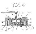
- the reference numeral 1 represents a rigid circuit board.
- a predetermined printed pattern circuit 2 is formed in the lower surface of the rigid circuit board 1.
- the reference numeral 3 represents an instrument movement such as a speedometer, an engine tachometer, or the like, attached to the upper surface of the rigid circuit board 1. Although the instrument movement 3 does not have a feature in internal configuration, the schematic configuration thereof will be described as follows.
- the reference numeral 4 represents a housing made of resin. The housing 4 also has a function as a coil bobbin. Inside the housing 4, a movable magnet 5 is rotatably supported through a pointer shaft 6. In addition, a pair of coils are wound and retained around the housing 4 perpendicularly to each other so as to form a cross coil 7.
- the reference numeral 8 represents a shield case disposed to cover the outside of the cross coil 7; 9, connection terminals connected to the cross coil 7; and 10, a pointer attached to a forward end of the pointer shaft 6.
- the instrument movement 3 configured thus is attached to the rigid circuit board 1
- the instrument movement 3 is put on the upper surface of the rigid circuit board 1.
- attachment holes 11 provided in the rigid circuit board 1 are made to agree with threaded holes 12 formed in the housing 4 of the instrument movement 3.
- attachment screws 13 are made to pass through the attachment holes 11 from the lower surface (back side) of the rigid circuit board 1. The attachment screws 13 are screwed down into the threaded holes 12 of the instrument movement 3 so that the rigid circuit board 1 and the instrument movement 3 are screwed to each other.
- the head of each attachment screw when the head of each attachment screw is immersed into the flow soldering tank, the head thereof might repel the solder to form the solder balls .
- the solder balls are attached to another soldering potion which might arise a loose connection in the circuit board 1.
- the IC, the resistor and the like except for the instrument movement 3 are flow-soldered in the flow soldering bath to electrically fix them to the circuit board 1.
- the instrument movement 3 is screwed and fixed to the circuit board 1, and then the terminals of the instrument movement 3 are spot-soldered with the wiring pattern of the circuit board 1 so that the instrument movement 3 is fixed and electrically connected with the circuit board 1. Therefore, the soldering of the instrument movement 3 and the soldering of other electronic components, such as an IC, a resistor and the like, have to be performed in separate steps, respectively. Two soldering steps are required in total.
- soldering is carried out by a robot without using the flow soldering tank as means for soldering the connection terminals 9 with the circuit portion of the rigid circuit board, it is possible to restrain generation of solder balls on the head portions of the attachment screws 13.
- robot soldering means it is necessary to solder respective portions to be soldered one by one. Therefore, it takes much time for soldering so that the assemblingproductivity deteriorates.
- the instrument movement 3 is fixed to the circuit board 1 through the resin engagement nail, and then the terminals of the instrument movement 3 are spot soldered with the printing pattern of the circuit board 1 so that the instrument movement 3 is fixed and electrically connected with the circuit board 1 without deformation of the resin engagement nail.
- the two soldering steps are also required in total.
- the present invention is made in consideration of such facts in the conventional. It is an object of the present invention to enable an electronic component such as an instrument movement or the like to be fixed to a rigid circuit board simply and easily without using any attachment screw when the electronic component is attached to the rigid circuit board, so that the number of man-hours for fastening attachment screws is omitted.
- an attachment structure of an electronic component to a circuit board comprising: a rigid circuit board having a suitable circuit pattern formed on a back surface thereof, having one or more attachment holes formed in the rigid circuit board for attachment of an electronic component, and further having soldering lands provided at circumferential edges of the attachment holes on the back surface of the rigid circuit board; an electronic component having one or more clip pass-through holes formed in positions in which the clip pass-through holes are coincident with the attachment holes correspondingly on a front surface of the rigid circuit board; and solderable clips for passing through the clip pass-through holes and the attachment holes correspondingly to perform fixed positioning of the electronic component to the rigid circuit board, each of the clips having an engagement portion portion at one end thereof and a pair of elastic engagement portions at the other end thereof, the engagement portion portion being engaged with a clip entrance side hole edge of corresponding one of the clip pass-through holes formed in the electronic component, the elastic engagement portions being engaged with a land formation surface side
- the attachment of the electronic component to the rigid circuit board can be ensured by the engagement force of the clips and the soldering between the clips and the lands provided on the rigid circuit board.
- the workability in attaching the electronic component to the rigid circuit board is improved on a large scale.
- a clip for fixing the electronic component to the rigid circuit board as defined in Claim 1 is characterized by comprising: a solderable and flexible/elastic metal piece which is bent into an V-shape along a longitudinal direction thereof and along a center thereof so as to form a bent piece; a pair of flexible/elastic pieces formed by forming a notch slit along a ridge line formed by bending the metal piece into the pair of bent pieces in the longitudinal direction and from a middle of the ridge line toward a forward end of the metal piece; engagement protrusions formed in vicinities of forward end portions of the flexible/elastic pieces, the engagement protrusions being inserted into and engaged with attachment holes formed in a rigid circuit board, respectively; and engagement portion formed at edges of the bent piece parallel to a ridge line of the bent piece and opposite to the flexible/elastic pieces of the bent piece, the engagement portion being pressed into and engaged with a clip pass-through hole formed in an electronic component.
- the rigid circuit board and the electronic component can be fixedly positioned by one touch.
- fixing the clip to the rigid circuit board by soldering it is possible to ensure the connection among the clip, the electronic component, and the circuit board.
- the workability in attachment of the electronic component to the rigid circuit board becomes excellent.
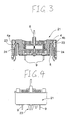
- Fig. 1 is an explanatory view showing the condition that an instrument movement 21 as an electronic component has been attached to a rigid circuit board 22 by use of clips 23.
- the electronic component 21 for use in the attachment structure according to the present invention is not limited to the instrument movement.
- the illustrated internal configuration of the instrument movement is substantially the same as that of the instrument movement described in the conventional art example. Therefore, constituent parts the same as those in the conventional art example are referenced correspondingly, and the description of the constituent parts will be omitted.
- arm portions 4a and 4b face with each other so that a pointer shaft 6 to be the center of the instrument movement 21 is located between the arm portions 4a and 4b, the arm portions 4a and 4b extending to the outside of a shield case 8.
- clip pass-through holes 24 are provided to penetrate the arm portions 4a and 4b from their surface sides to their back surface sides respectively.
- a plurality of attachment holes 25a and 25b are provided to be located correspondingly to the clip pass-through holes 24.
- a plurality of terminal insertion holes 26 are provided so as to be penetrated by connection terminals 9 provided in the rigid circuit board 22.
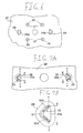
- the pair of attachment holes 25a and 25b are formed in the rigid circuit board 22 as substantially triangular holes corresponding to the sectional external shapes of clips 23 which will be described later.
- a pair of attachment holes 25a and 25b are formed as a pair of substantially triangular holes so that one side of one triangular hole is opposite to and parallel to one side of the other triangular hole, the triangular holes 25a and 25b being located so as to be axially symmetrical.
- terminal soldering lands 27 are formed at the circumferential edges of the terminal insertion holes 26.
- clip soldering lands 28 are formed at the circumferential edges of the attachment holes 25a and 25b respectively.
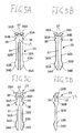
- each of the clips 23 is formed of a flexible/elastic metal plate of a solderable material such as brass by pattern-draw press means.
- the metal plate with the shorter side at the top is bent into an V-shape so that a ridge line 29 is formed along its longitudinal center.
- two bent pieces 30A and 30B are formed.
- the metal plate is notched from the middle of the ridge line 29 toward the forward end so that a slit 31 is formed along the ridge line 29 formed by bending the metal plate in the longitudinal direction.
- a pair of flexible/elastic pieces 32A and 32B are formed respectively.
- engagement protrusions 34A and 34B are formed to have inclined edges 33A and 33B projecting outward in the direction opposite to the slit 31.
- the end portions of the two bent pieces 30A and 30B opposite to the flexible/elastic pieces 32A and 32B are bent outward at right angles so as to form engagement collars 35A and 35B respectively.
- engagement portion 36 are formed to be pressed into and engaged with the clip pass-through holes 24 formed in the electronic component 21.
- protrusions 37 are formed by press work.
- the protrusions 37 operate to prevent respective clips put on top of one another from coming into close contact, and make the clips easy to be handled one by one.
- the rigid circuit board 22, the electronic component 21 and the clips 23 are configured thus according to the present invention. Next, description will be made about the procedure of attaching the electronic component 21 onto the rigid circuit board 22 by use of the clips 23.
- the forward ends of the clips 23 on the sides of the engagement protrusions 34A and 34B are inserted respectively from above the corresponding clip pass-through holes 24 formed in the electronic component 21.
- the clips 23 are pressed into the clip pass-through holes 24 entirely so that the clip forward ends project from the lower end surface of the electronic component 21.
- the engagement collars 35A and 35B formed in each of the clips 23 are brought into contact and engaged with the upper surface of the electronic component 21 while the engagement portion 36 formed in each of the clips 23 are pressed into and engaged with the inner surfaces of the clip pass-through holes 24.
- the clips 23 are fixedly attached to the electronic component 21.
- the pair of clips 23 are attached to the movement 21 so that the ridge lines 29 of the clips 23 are located to face outside, and the sides of the clips opened in V-shapes are directed inside to be opposed to each other.
- the lower surface of the electronic component 21 to which the clips 23 have been fixedly attached is laid on the upper surface of the rigid circuit board 22.
- the engagement protrusions 34A and 34B at the forward ends of the clips 23 fixedly attached to the electronic component 21 are passed through the attachment holes 25a and 25b formed in the rigid circuit board 22.
- the engagement protrusions 34A and 34B are engaged with the back-side hole edges of the attachment holes 25a and 25b by use of the elastic restitution force of the flexible/elastic pieces 32A and 32B.
- the connection terminals 9 provided in the electronic component are inserted into the terminal insertion holes 26 provided in the rigid circuit board 22 after the forward ends of the clips 23 have been inserted and positioned into the attachment holes 25a and 25b formed in the rigid circuit board 22.
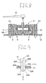
- the inclined edges 33A and 33B forming the two engagement protrusions 34A and 34B are brought into elastic contact with the back-side hole edges of the attachment holes 25a and 25b as shown in Fig. 9.
- the engagement protrusions 34A and 34B brought into contact with the back-side hole edges of the attachment holes 25a and 25b by the elastic pressure of the flexible/elastic pieces 32A and 32B generate a force acting in the downward direction (Z).
- the lower surface of the electronic component 21 is brought into contact with the upper surface of the rigid circuit board 22 through the clips 23 without looseness so that the electronic component 21 is positioned on the rigid circuit board 22 stably.
- the clips 23 are designed to be bent in the V-shapes and to be engaged with the triangular attachment holes 25a and 25b formed in the rigid circuit board 22. Accordingly, not only does a force act in the Z-direction but also a force acts horizontally in a direction opposite to the X-direction and the Y-direction, as shown in Figs. 7A and 7B. Further, in this embodiment, a pair of clips 23 are disposed so that the ridge lines 29 thereof are located to face outside while the sides of the clips 23 opened in the V-shapes are opposed to each other. Accordingly, forces acting in the X-direction shown in Fig. 7A act in direction in which the clips 23 are opposite to each other. Thus, the movement 21 is supported and held also horizontally on the rigid circuit board 22 so that the movement 21 can be retained more firmly.
- the rigid circuit board 22 on which the electronic component 21 has been positioned thus has the lower surface immersed in molten solder in a flow soldering tank (not shown) .
- soldering is carried out between the connection terminals 9 and the terminal soldering lands 27 provided on the back surface (lower surface) of the rigid circuit board 22, and between the protrusion portions at the forward ends of the clips 23 and the clip soldering lands 28 provided on the back surface (lower surface) of the rigid circuit board 22.
- the fixation (attachment) of the electronic component 21 to the rigid circuit board 22 is ensured through the clips 23 fixed to the rigid circuit board 22.
- reference numerals 40 in Fig. 1 represent soldered portions which solder the connection terminal 9 with the terminal soldering land 27, or which solder the forward end of the clip 23 with the clip soldering land 28.
- the clips are inserted into the clip pass-through holes 24 formed in the electronic component 21, and the attachment holes formed in the rigid circuit board 22, so as to ensure the positioning between the electronic component 21 and the rigid circuit board 22. Further, the clips are fixed to the electronic component 21 and the rigid circuit board 22 by soldering so that the fixation between the electronic component 21 and the rigid circuit board 22 is maintained. Accordingly, the work (step) of fastening attachment screws in the conventional art can be omitted. Thus, the workability in attachment of the electronic component to the rigid circuit board is improved on a large scale.
- each of the clips 23 used in this embodiment is designed to have a pair of flexible/elastic pieces 32A and 32B which are provided with inclined edges 33A and 33B in the forward ends of the flexible/elastic pieces 32A and 32B respectively. Accordingly, at the time of the engagement operation by the clips 23, the inclined edges 33A and 33B of the clips 23 are brought into elastic contact with the lower surface hole edges of the attachment holes 25a and 25b. As a result, the clips 23 are urged to bring the lower surface of the electronic component 21 into pressure contact with the upper surface of the rigid circuit board 22. Thus, by use of the clips 23, it is possible to ensure the positioning between the electronic component 21 and the rigid circuit board 22.
- the clips are inserted from above so that the rigid circuit board is attached to the lower surface side of the electronic component.
- the present invention is not limited to this embodiment.
- the attachment hole 25a and 25b may be formed above the electronic component 21, in which the soldering land and the printed pattern face upward. In such a case, the clips are inserted from below the electronic component 21.
- the attachment of the electronic component to the rigid circuit board can be ensured by the engagement force of the clips and the soldering between the clips and the lands provided on the rigid circuit board.
- the workability in attachment of the electronic component to the rigid circuit board is improved on a large scale.
- fixation and positioning between the rigid circuit board and the electronic component can be achieved by one touch.
- the clips and the rigid circuit board are fixed by soldering.
- the connection among the clips, the electronic component and the circuit board can be ensured so that the workability in attachment of the electronic component to the rigid circuit board becomes superior.
- the movement and electronic components such as an IC and resistor can be flow-soldered at the same time by the use of the metal clips of the invention.
Landscapes
- Engineering & Computer Science (AREA)
- Physics & Mathematics (AREA)
- General Physics & Mathematics (AREA)
- Microelectronics & Electronic Packaging (AREA)
- Manufacturing & Machinery (AREA)
- Combinations Of Printed Boards (AREA)
Abstract
Description
Claims (21)
- An attachment structure comprising:a circuit board having a first surface and a second surface, the circuit board having an attachment hole;an electronic component disposed on the first surface of the circuit bard, the electronic component having a pass-through hole; anda clip for passing through the pass-through hole and the attachment hole,wherein the circuit board is soldered with the clip to fix and position the electronic component to the circuit board.
- The attachment structure as claimed in claim 1, wherein the clip has an engagement portion portion at a first end of the clip, the engagement portion being engaged with the clip entrance side hole edge of the pass-through hole of the electronic component.
- The attachment structure as claimed in claim 1, wherein the clip has an elastic engagement portion at a second end of the clip, the elastic engagement portion being engaged with the hole edge of the attachment hole of the circuit board.
- The attachment structure as claimed in claim 3, wherein the elastic engagement portion is engaged with the hole edge at the second surface of the circuit board.
- The attachment structure as claimed in claim 4, wherein the elastic engagement portion is elastically displaceable in the diameter direction of the attachment hole.
- The attachment structure as claimed in claim 1, wherein the circuit board has a wiring pattern on the second surface, and the clip is soldered on the second surface.
- The attachment structure as claimed in claim 6, wherein the circuit board includes a soldering land provided at the circumferential edge of the attachment hole on the second surface of the circuit board, and the clip is soldered at the soldering land.
- The attachment structure as claimed in claim 1, wherein the circuit board is rigid.
- The attachment structure as claim in claim 1, wherein the attachment hole comprises a plurality of attachment holes formed in the circuit board, and the soldering land comprises a plurality of soldering lands provided at the circumferential edge of each of the attachment holes on the second surface of the circuit board.
- The attachment structure as claimed in claim 1, wherein the clip is made of metal.
- The attachment structure as claimed in claim 1, wherein the clip has two bent pieces formed by being bent in a V-shape along with a center line of the clip.
- The attachment structure as claimed in claim 11, wherein the clip defines a slit along with the centerline of clip to have two flexible pieces in the two bent pieces, respectively.
- The attachment structure as claimed in claim 1, wherein the clip has a press-fitting protrusion inserted into the path-through hole and press-fitted with the inner surface of the path-through hole of the electronic component.
- The attachment structure as claimed in claim 1, wherein the elastic engagement portion has a slope portion engaged with the hole edge of the attachment hole.
- A clip used in attachment of an electronic component to a circuit board, the clip for passing through a pass-through hole of the electronic component and an attachment hole of the circuit board, wherein the circuit board is soldered with the clip to fix and position the electronic component to the circuit board, the clip comprising:an engagement portion portion at a first end of the clip, the engagement portion being engaged with the clip entrance side hole edge of the pass-through hole of the electronic component;an elastic engagement portion at a second end of the clip, the elastic engagement portion being engaged with the hole edge of the attachment hole of the circuit board.
- The clip as claimed in claim 15, wherein the elastic engagement portion is elastically displacable in the diameter direction of the attachment hole.
- The clip as claimed in claim 15, wherein the clip is made of metal.
- The clip as claimed in claim 15, further comprising two bent pieces formed by being bent in a V-shape along with a center line of the clip.
- The clip as claimed in claim 15, further comprising a slit along with the centerline of clip to have two flexible pieces in the two bent pieces, respectively.
- The clip as claimed in claim 15, further comprising a press-fitting protrusion to be inserted into the path-through hole of the electronic component and press-fitted with the inner surface of the path-through hole of the electronic component.
- The clip as claimed in claim 15, wherein the elastic engagement portion has a slope portion engaged with the hole edge of the attachment hole.
Applications Claiming Priority (2)
| Application Number | Priority Date | Filing Date | Title |
|---|---|---|---|
| JP2000143635 | 2000-05-16 | ||
| JP2000143635 | 2000-05-16 |
Publications (2)
| Publication Number | Publication Date |
|---|---|
| EP1156710A2 true EP1156710A2 (en) | 2001-11-21 |
| EP1156710A3 EP1156710A3 (en) | 2004-06-16 |
Family
ID=18650426
Family Applications (1)
| Application Number | Title | Priority Date | Filing Date |
|---|---|---|---|
| EP01111765A Withdrawn EP1156710A3 (en) | 2000-05-16 | 2001-05-15 | Attachment structure of electronic component to circuit board and clip used in attachment of the electronic component |
Country Status (2)
| Country | Link |
|---|---|
| US (1) | US6490164B2 (en) |
| EP (1) | EP1156710A3 (en) |
Families Citing this family (4)
| Publication number | Priority date | Publication date | Assignee | Title |
|---|---|---|---|---|
| JP4751469B2 (en) * | 2009-12-04 | 2011-08-17 | 株式会社東芝 | Electronics |
| US20120269599A1 (en) * | 2011-04-20 | 2012-10-25 | Shayan Malek | Threaded structures with solder management features |
| JP1578442S (en) * | 2016-10-06 | 2017-06-05 | ||
| JP1577870S (en) * | 2016-10-06 | 2017-06-05 |
Family Cites Families (8)
| Publication number | Priority date | Publication date | Assignee | Title |
|---|---|---|---|---|
| FR2353970A1 (en) * | 1976-06-03 | 1977-12-30 | Chauchat Jean | Thin panel mounting for rectangular electronic components - uses sprung clip gripping component and having arrow head ends passing through circuit board |
| FR2580892B1 (en) * | 1985-04-23 | 1988-07-15 | Alsthom Cgee | METHOD FOR ATTACHING A CONNECTOR TO THE SUBSTRATE OF A PRINTED CIRCUIT BY A PIONE FOR ATTACHING THIS CONNECTOR TO THE SUBSTRATE |
| MY107281A (en) * | 1989-11-02 | 1995-10-31 | Whitaker Corp | Retaining device for electrical connectors. |
| US5241453A (en) * | 1991-11-18 | 1993-08-31 | The Whitaker Corporation | EMI shielding device |
| JPH07312473A (en) * | 1994-05-18 | 1995-11-28 | Toshiba Fa Syst Eng Kk | Wiring board unit and method of manufacturing wiring board unit |
| US5580203A (en) * | 1994-12-21 | 1996-12-03 | General Instrument Corporation Of Delaware | Resilient snap fitting retainer for printed circuit board mounting or the like |
| US6201697B1 (en) * | 1999-02-16 | 2001-03-13 | Chip Coolers, Inc. | Heat sink assembly with cam lock |
| US6219244B1 (en) * | 2000-03-28 | 2001-04-17 | Yang-Shiau Chen | Securing fixture for a heat sink for a CPU |
-
2001
- 2001-05-15 US US09/854,478 patent/US6490164B2/en not_active Expired - Fee Related
- 2001-05-15 EP EP01111765A patent/EP1156710A3/en not_active Withdrawn
Also Published As
| Publication number | Publication date |
|---|---|
| EP1156710A3 (en) | 2004-06-16 |
| US6490164B2 (en) | 2002-12-03 |
| US20010043464A1 (en) | 2001-11-22 |
Similar Documents
| Publication | Publication Date | Title |
|---|---|---|
| US6396001B1 (en) | Printed circuit board and method of making the same | |
| JPH0411349Y2 (en) | ||
| KR101504696B1 (en) | Contact device for fastening to a circuit board, method for fastening a contact device to a circuit board, and circuit board | |
| JP4697163B2 (en) | Electronic equipment | |
| US20060216970A1 (en) | Electrical connector terminal and method of producing same | |
| JPH08203487A (en) | Battery terminal for small electronic devices and its holding structure | |
| US6280205B1 (en) | Surface-mounted type connector and method for producing circuit device including the same | |
| US6490164B2 (en) | Attachment structure of electronic component to circuit board and clip used in attachment of the electronic component | |
| EP1211921A2 (en) | Part for soldering to a printed wiring board | |
| US6510060B2 (en) | Electrical subassembly having a holding device and an electrical component fastened thereto | |
| US6163461A (en) | Terminal mounting structure for a printed circuit board | |
| JP2004039742A (en) | Temporary fixing parts | |
| KR980007880A (en) | Electrical conductor | |
| JPH0710973U (en) | Mounting structure of integrated circuit board | |
| US20240413570A1 (en) | Contact-making arrangement, electronics assembly and method for assembling an electronics assembly | |
| CN108023014B (en) | Electronic component | |
| JP2008282958A (en) | Electrical connection terminal for connection hole and locking structure of electronic component provided with the same | |
| US7222543B2 (en) | Modular encoder, method of producing a modular encoder, and system for measuring angular movement | |
| JPS60254785A (en) | Spacer for electronic element | |
| US20250385024A1 (en) | Wire holding structure and electronic device | |
| EP4475344A1 (en) | Connector and electronic assembly | |
| JPS62278776A (en) | Plating connector for electric or electronic element | |
| JP2537787B2 (en) | Power supply | |
| JPS5926289Y2 (en) | Printed circuit board inspection jig | |
| JP2005228716A (en) | Socket for electronic parts |
Legal Events
| Date | Code | Title | Description |
|---|---|---|---|
| PUAI | Public reference made under article 153(3) epc to a published international application that has entered the european phase |
Free format text: ORIGINAL CODE: 0009012 |
|
| AK | Designated contracting states |
Kind code of ref document: A2 Designated state(s): AT BE CH CY DE DK ES FI FR GB GR IE IT LI LU MC NL PT SE TR |
|
| AX | Request for extension of the european patent |
Free format text: AL;LT;LV;MK;RO;SI |
|
| PUAL | Search report despatched |
Free format text: ORIGINAL CODE: 0009013 |
|
| AK | Designated contracting states |
Kind code of ref document: A3 Designated state(s): AT BE CH CY DE DK ES FI FR GB GR IE IT LI LU MC NL PT SE TR |
|
| AX | Request for extension of the european patent |
Extension state: AL LT LV MK RO SI |
|
| 17P | Request for examination filed |
Effective date: 20041206 |
|
| AKX | Designation fees paid |
Designated state(s): DE FR GB |
|
| 17Q | First examination report despatched |
Effective date: 20080521 |
|
| STAA | Information on the status of an ep patent application or granted ep patent |
Free format text: STATUS: THE APPLICATION IS DEEMED TO BE WITHDRAWN |
|
| 18D | Application deemed to be withdrawn |
Effective date: 20081002 |