EP1156490A1 - Semiconductor integrated circuit, ink cartridge having this semiconductor integrated circuit, and ink jet recording device mounted with this ink cartridge - Google Patents
Semiconductor integrated circuit, ink cartridge having this semiconductor integrated circuit, and ink jet recording device mounted with this ink cartridge Download PDFInfo
- Publication number
- EP1156490A1 EP1156490A1 EP00964674A EP00964674A EP1156490A1 EP 1156490 A1 EP1156490 A1 EP 1156490A1 EP 00964674 A EP00964674 A EP 00964674A EP 00964674 A EP00964674 A EP 00964674A EP 1156490 A1 EP1156490 A1 EP 1156490A1
- Authority
- EP
- European Patent Office
- Prior art keywords
- signal line
- writing
- semiconductor integrated
- integrated circuit
- input
- Prior art date
- Legal status (The legal status is an assumption and is not a legal conclusion. Google has not performed a legal analysis and makes no representation as to the accuracy of the status listed.)
- Withdrawn
Links
Images






Classifications
-
- G—PHYSICS
- G11—INFORMATION STORAGE
- G11C—STATIC STORES
- G11C17/00—Read-only memories programmable only once; Semi-permanent stores, e.g. manually-replaceable information cards
-
- B—PERFORMING OPERATIONS; TRANSPORTING
- B41—PRINTING; LINING MACHINES; TYPEWRITERS; STAMPS
- B41J—TYPEWRITERS; SELECTIVE PRINTING MECHANISMS, i.e. MECHANISMS PRINTING OTHERWISE THAN FROM A FORME; CORRECTION OF TYPOGRAPHICAL ERRORS
- B41J2/00—Typewriters or selective printing mechanisms characterised by the printing or marking process for which they are designed
- B41J2/005—Typewriters or selective printing mechanisms characterised by the printing or marking process for which they are designed characterised by bringing liquid or particles selectively into contact with a printing material
- B41J2/01—Ink jet
- B41J2/17—Ink jet characterised by ink handling
- B41J2/175—Ink supply systems ; Circuit parts therefor
- B41J2/17503—Ink cartridges
- B41J2/17553—Outer structure
-
- B—PERFORMING OPERATIONS; TRANSPORTING
- B41—PRINTING; LINING MACHINES; TYPEWRITERS; STAMPS
- B41J—TYPEWRITERS; SELECTIVE PRINTING MECHANISMS, i.e. MECHANISMS PRINTING OTHERWISE THAN FROM A FORME; CORRECTION OF TYPOGRAPHICAL ERRORS
- B41J2/00—Typewriters or selective printing mechanisms characterised by the printing or marking process for which they are designed
- B41J2/005—Typewriters or selective printing mechanisms characterised by the printing or marking process for which they are designed characterised by bringing liquid or particles selectively into contact with a printing material
- B41J2/01—Ink jet
- B41J2/17—Ink jet characterised by ink handling
- B41J2/175—Ink supply systems ; Circuit parts therefor
- B41J2/17503—Ink cartridges
- B41J2/1752—Mounting within the printer
- B41J2/17523—Ink connection
-
- B—PERFORMING OPERATIONS; TRANSPORTING
- B41—PRINTING; LINING MACHINES; TYPEWRITERS; STAMPS
- B41J—TYPEWRITERS; SELECTIVE PRINTING MECHANISMS, i.e. MECHANISMS PRINTING OTHERWISE THAN FROM A FORME; CORRECTION OF TYPOGRAPHICAL ERRORS
- B41J2/00—Typewriters or selective printing mechanisms characterised by the printing or marking process for which they are designed
- B41J2/005—Typewriters or selective printing mechanisms characterised by the printing or marking process for which they are designed characterised by bringing liquid or particles selectively into contact with a printing material
- B41J2/01—Ink jet
- B41J2/17—Ink jet characterised by ink handling
- B41J2/175—Ink supply systems ; Circuit parts therefor
- B41J2/17503—Ink cartridges
- B41J2/17543—Cartridge presence detection or type identification
- B41J2/17546—Cartridge presence detection or type identification electronically
-
- G—PHYSICS
- G11—INFORMATION STORAGE
- G11C—STATIC STORES
- G11C7/00—Arrangements for writing information into, or reading information out from, a digital store
- G11C7/22—Read-write [R-W] timing or clocking circuits; Read-write [R-W] control signal generators or management
Definitions
- the present invention relates to a semiconductor integrated circuit, an ink cartridge having the semiconductor integrated circuit, and an inkjet recording device having the ink-cartridge attached, more particularly, to a semiconductor integrated circuit having a non-volatile memory built in and using boosted voltage for data writing, an ink cartridge having the semiconductor integrated circuit, and an inkjet recording device having the ink cartridge attached.
- such a semiconductor integrated circuit performs a write operation by using voltage boosted by an internal booster circuit when writing data to a built-in, non-volatile memory.
- charges integrated in a signal line charged at the time of writing is discharged before shifting to the next writing operation.
- the discharging is performed by a discharge circuit within the semiconductor integrated circuit.
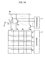
- Fig. 13 is a circuit diagram showing a discharge circuit in a conventional semiconductor integrated circuit. As shown in Fig. 14, the discharge circuit discharges charges integrated in a parasitic capacity Cx associated with a signal line to a memory cell array 5.
- the parasitic capacity Cx is charged in the following manner:
- An address counter 2 performs a count operation in response to an input of a write signal WR so that an address decoder whose input is the count value operates.
- the address decoder 103 includes a column decoder 4 and a row decoder 3 for specifying a column and a row of memory cells forming a memory cell array 5, respectively.
- the memory cell array 5 includes a plurality of memory cells arranged in n rows by m columns.
- Each of outputs of the column decoder 4, that is the decoded result, is input to respective gate terminals of transistors Tr1, Tr2,... and Trm which are switching elements.
- the source terminal of each transistor is connected to a data wire DW while the drain terminal is connected to a signal line corresponding to a respective column of memory cells in the memory cell array 5. Therefore, by turning any one of transistors Tr1, Tr2,...and Trm to the ON status with the output of the column decoder 4, a signal line corresponding to a respective column is charged by voltage of the data wire DW through the respective transistor.
- charges are integrated in a parasitic capacity of the signal line corresponding to the column specified by the column decoder 4. For example, when the transistor Tr1 is turned ON, charges are integrated in the parasitic capacity of the signal line including a node A.
- the input/output control circuit 8 includes an internal booster circuit 107 for boosting the voltage of a power supply V DD in response to an input of the write signal WR, an inverter for generating an inverted signal of the write signal WR, a switching transistor 106 to whose gate terminal is supplied with the output of the inverter 105, that is the inverted signal of the write signal WR, and a buffer 108 having a boosted output V PP as a power supply and supplying voltage corresponding to a value of a data input I/O to the data wire DW.
- the write signal WR is at high level when writing to a memory cell while the transistor 106 is in the OFF condition.
- the power supply V DD is supplied to the internal booster circuit 107, resulting in a higher potential (15 volt, for example) of the boosted output V PP .
- the potential is supplied to the buffer 108 as a power supply.
- voltage corresponding to a value of the data input I/O is supplied from the buffer 108 to the data wire DW.
- a signal wire corresponding to the respective column is charged by the voltage of the data wire DW through the transistor.
- the condition where the signal line is charged the condition where charges are integrated
- data is written in each one of memory cells within the memory cell array 5 by the sequential changes in the outputs of the row decoder 3.
- the write signal WR is at the low level, and the transistor 106 is turned ON.
- the power supply V DD is not supplied to the internal booster circuit 107, which turns the boosted output V PP to the low potential (5 volt, for example).
- the output of the buffer 108 to which the potential is supplied as the power supply is turned to the low level regardless of the value of the data input I/O. Therefore, the above-described integrated charges are discharged through the data wire DW to which the output of the buffer 108 is supplied. For example, the charges integrated in the parasitic capacity Cx at node A shown are discharged toward ground applied to the buffer 108.
- the transistor Tr1 when writing to the X1 column of memory cells, the transistor Tr1 is turned ON by the column decoder 4, first of all, and the parasitic capacity Cx at node A is charged. In the charged condition, writing is performed by the row decoder 3 in the sequence of row Y1, row Y2...to row Yn. When the writing is completed at row Yn, the parasitic capacity Cx is discharged as described above. After the discharging, the transistor Tr2 corresponding to a next column X2 is turned ON by the column decoder 4, and the next parasitic capacity Cx is charged. In the charged condition, writing is performed by the row decoder 3 in the sequence of row Y1, row Y2...to row Yn.
- Charging and discharging are repeatedly performed on the other signal lines in similar manner. Through this operation, each 1 bit is specified in order from column X1 and row y1 to column Xm and row Yn, and then writing is performed on all bits included in the memory cell array 5.
- a purpose of the present invention is to provide a semiconductor integrated circuit having a discharge circuit, which can surely discharge, an ink cartridge using it, and an inkjet recording device having the cartridge.
- a semiconductor integrated circuit includes a charge unit for charging a signal line corresponding to each 1 row in response to an input of a writing instruction for each bit of a memory cell arranged in n rows by m columns (where n and m are natural numbers and so forth) and charging a signal line corresponding to a next row after writing on all bits for one column is completed.
- the semiconductor integrated circuit performs writing on each 1 bit sequentially in each of bits for 1 column corresponding to the signal line charged by the charge unit.
- the semiconductor integrated circuit includes a delay unit for delaying an input of the writing instruction to the charge unit for at least a time equivalent to a discharge time for the signal line.
- Another semiconductor integrated circuit includes a charge unit for charging a signal line corresponding to each 1 row in response to an input of a writing instruction for each bit of a memory cell arranged in n rows by m columns and charging a signal line corresponding to a next row after writing on all bits for one column is completed.
- the semiconductor integrated circuit performs writing on each 1 bit sequentially in each of bits for 1 column corresponding to the signal line charged by the charge unit.
- the semiconductor integrated circuit includes a suppressing unit for suppressing a change in address indicating a cell to be written within a predetermined time after completing the writing for 1 bit.
- the suppressing unit may be a delay circuit for delaying an input of the writing instruction to the charge unit for at least a time equivalent to a discharge time for the signal line.
- Another semiconductor integrated circuit includes a charge unit for charging a signal line corresponding to each 1 row in response to an input of a writing instruction for each bit of a memory cell arranged in n rows by m columns and charging a signal line corresponding to a next row after writing on all bits for one column is completed.
- the semiconductor integrated circuit performing writing on each 1 bit sequentially in each of bits for 1 column corresponding to the signal line charged by the charge unit.
- the semiconductor integrated circuit includes a delay unit for differentiating timing for completing writing for 1 bit and timing for changing an address indicating a cell to be written for a time equivalent to a time for charging at least the signal line.
- the above-described charge unit comprises a counter for starting an count operation in response to an input of the writing instruction, a column decoder for decoding a count value of the counter, a switching element for charging the signal line by connecting a predetermined power supply to the signal line after turned ON depending on a decoding result by the decoder, and a row decoder for specifying each 1 bit sequentially for 1 row of bits corresponding to the signal line charged when the switching element is turned ON.
- An ink cartridge according to the present invention has the above-described semiconductor integrated circuit, for storing at least a remained amount of ink on the memory cell.
- An inkjet recording device has the above-described ink cartridge for printing desired image information by using ink supplied from the ink cartridge.
- Fig. 1 is a circuit diagram showing the structure of an example of a discharge circuit within a semiconductor integrated circuit according to the present invention.
- the discharge circuit shown in the figure is different from the conventional circuit shown in Fig. 13, and a delay circuit 10 is inserted before the address counter 2. Further, an AND gate 109 is provided instead of buffer 108.
- input of a write signal WR to the address counter 2 can be delayed by the delay circuit 10. That is, by delaying the update timing of an address after writing, it is arranged to perform discharge from a column selecting transistor through the AND gate 109. More specifically, the discharge is performed through a transistor in the output stage of the AND gate 109.
- the discharge time can get a margin by delaying the address updating timing for a predetermined amount of time with respect to the transition timing of the write signal.
- the discharge speed depends on the driving capability (equivalent resistance), and the delay time can be calculated as the product of an equivalent resistance R and a capacity Cx, that is, a time constant. Further, in order to reduce the size of the circuit as much as possible, it is convenient to keep the insertion of the delay circuit 10 at one point. Thus, in this embodiment, it is provided at a position before the address counter 2 (input side).
- Fig. 2 is a functional block diagram for describing the internal structure of a semiconductor integrated circuit using the discharge circuit shown in Fig. 1.
- semiconductor integrated circuit 1 includes an address counter 2 for performing an count operation, a row decoder 3 and a column decoder 4 for decoding a count value in the address counter 2 in order to create an address, the memory cell array 5 for storing data, a write/read control circuit 6 for controlling a latch circuit 7 and a buffer B depending on writing into or reading out of the memory cell array 5, the latch circuit 7 controlled by the write/read control circuit 6 to assume a latch status or a through status, the input/output control circuit 8 for controlling input and output of data to the memory cell array 5, AND gates G1 to G3, and the delay circuit 10 for delaying write signals. Further, the semiconductor integrated circuit 1 is provided with external terminals P1 to P6.
- the count value of the address counter 2 is initialized to a predetermined value based on the inverted signal of a chip-select input signal CS input to the external terminal P1. Further, the address counter 2 creates updated address data based on a signal input from the AND gate G1. The created address data is input to the row decoder 3 and the column decoder 4.
- the column decoder 4 selects the column including the desired memory cell in the memory cell array 5 based on address data input from the address counter 2.
- the row decoder 3 selects the row including the desired memory cell in the memory cell array 5 based on the address data input from the address counter 2.
- the memory cell array 5 is formed by arranging a plurality of memory cells in a matrix. Each memory cell in an addressed row is turned to an ON status by a select signal from the row decoder 3, while a select signal from the column decoder 4 enables information stored in the memory cell to be read and written. In this case, it is assumed that the memory cell array 5 is formed by non-volatile memory cells.
- the write/read control circuit 6 determines whether writing or reading is performed on the memory cell array 5 based on the chip-select control signal CS input to the external terminal P1 and signals output from an AND gate G2 or G3.
- the output of the AND gate G2 is write signal WR.
- the latch circuit 7 outputs read data of the memory cell array 5, which is output from the input/output control circuit 8, to an external terminal P6 after keeping it for a predetermined period of time based on a control signal from the write/read control circuit 6.
- the latch circuit 7 performs either a latch operation or a through operation depending on the output of the write/read control circuit 6.
- the latch circuit 7 performs the latch operation when the output of the write/read control circuit 6 is at the low level, whereas the latch circuit 7 performs the through operation when the output of the write/read control circuit 6 is at the high level.
- the latch operation is an operation for maintaining the output status.
- the through operation is an operation for sending out the input signal as an output signal as it is.
- the input/output control circuit 8 writes, into the memory cell array 5, data input to the external terminal P6, or conversely, outputs read-out data to the external terminal P6 through the latch circuit 7.
- the input/output control circuit 8 is operated by the write signal WR.
- the write signal WR is input to the address counter 2 after being delayed by the delay circuit 10.
- the delay time of the delay circuit 10 is a time substantially equal to the time for discharging charges accumulated on the above-described parasitic capacity Cx. According to the structure above, data writing is performed on the memory cell array 5.
- the written data is, for example, a remaining amount of ink. By writing the amount of remaining ink, the remaining amount of ink can be always monitored.
- the AND gate G1 outputs, to the address counter 2 and the AND gate G2 or G3, a signal which is the conjunction of the chip-select control signal CS input via the external terminal P1 and a clock input signal CK input via the external terminal P2.
- the AND gate G2 outputs, to the write/read control circuit 6, a signal which is the conjunction of the output signal from the AND gate G1 and a write/read input signal W/R from the external terminal P3.
- the AND gate G3 outputs, to the write/read control circuit 6, a signal which is the conjunction of the output signal from the AND gate G1 and the inverted signal of the write/read input signal W/R from the external terminal P3.
- the external terminal P1 is a terminal for inputting the chip-select input signal CS, that is a control signal STB for selecting a specific device when a plurality of devices exist at the same time, for initializing the address counter 2, and for shifting the operation mode. That is, the external terminal P1 in this embodiment is a terminal used both as a control terminal for initializing an address counter and as a control terminal for shifting the operation mode.
- the external terminal P2 is a terminal for inputting the clock input signal CK that is a reference for the semiconductor integrated circuit 1 to operate.
- the external terminal P3 is a terminal for inputting the write/read input signal W/R for specifying an access operation on the memory cell array 5 built in the semiconductor integrated circuit 1.
- the external terminals P4 and P5 are input terminals for applying operational voltage at a high potential voltage level V DD and at a low potential voltage level V SS for the semiconductor integrated circuit 1 to operate.
- the external terminal P6 is an input/output terminal for inputting data to be actually written into the memory cell array 5 built in the semiconductor integrated circuit 1 and/or for outputting data read out from the memory cell array 5.
- Fig. 3 is a timing chart for describing a readout operation on the semiconductor integrated circuit.
- Fig.2 shows the chip-select control signal CS, the write/read input signal W/R, the clock CLOCK, the count values of the address counter 2, and the input/output signals I/O at the external terminal P6 in Fig. 2.
- "L" is applied to the external terminal P1, first of all, to initialize the address counter 2.
- "H” is applied to the external terminal P1, and clock pulses for an intended readout start address are input via the external terminal P2.
- "L” for specifying the readout is applied as a write/read input signal W/R to the external terminal P3.
- the address corresponding to data to be read is output in a period when the clock-input signal CK is turned to "L". During the period when the clock input signal CK is "H”, the data is maintained since it is latched within the latch circuit 7 at the leading edge. At the trailing edge, the address is incremented, and data for the next address is output from the external terminal P6.
- Fig. 4 is a timing chart for describing a write operation on the semiconductor integrated circuit, for example.
- Fig. 4 shows the chip-select control signal CS, the write/read input signal W/R, the clock CLOCK, the count values of the address counter 2, and the input/output signals I/O at the external terminal P6.
- "L" is applied to the external terminal P1 in a condition where the write/read input signal W/R is "L” in order to initialize the address counter 2.
- "H" is applied to the external terminal P1, and clock pulses for an intended write start address are input via the external terminal P2.
- "H" for specifying the write is applied as the write/read input signal W/R to the external terminal P3.
- the stand-by signal STB for the operation mode shifting is turned to "L", and the operation mode of the semiconductor integrated circuit 1 is shifted to the stand-by mode.
- the operation mode of the semiconductor integrated circuit 1 is shifted to the stand-by mode, operation of parts where current flows steadily is terminated to achieve a reduction of the current consumption.
- the sense amplifier provided within the input/output control circuit 8 for example, always needs current flow. Therefore, in order to suppress power consumption in the present circuit in the stand-by mode, the source voltage to supplied to the input/output control circuit 8 is turned to OFF.
- the address counter 2 is initialized and the semiconductor integrated circuit 1 is shifted to the stand-by mode. Since these instructions are controlled by inputs to the external terminal P1, that is a dual-usage terminal, the memory initialization function and the function for shifting to the stand-by mode are provided, achieving a reduction of the number of external terminals. Further, the control terminal for the memory initialization and the control terminal for operation mode control are combined to one dual-usage terminal, which makes the control easier.
- the functions for the circuit block initialization and the operation mode shifting may be arranged such that the address counter 2 is initialized and the semiconductor integrated circuit 1 is shifted to the stand-by mode when the logical operation between the input to the external terminal P1 and the input to other terminals is in the unselected condition.
- Fig. 5 is a timing chart showing timing for address changes for write signals in the conventional circuit and the present circuit, respectively.
- voltage of the data wire DW is changed synchronously with the timing of leading and trailing edges of the write signals WR.
- the voltage alternates between 0 volt and 15 volt.
- the delay circuit 10 since the delay circuit 10 is not provided, the content at an address ADBS1 is changed synchronously with the trailing edge of the voltage waveform of the data wire DW.
- the address is changed before discharge of integrated charges in the parasitic capacity is completed, and wrong writing may be performed.
- the delay circuit 10 since the delay circuit 10 is provided in the present circuit, the content of an address ADRS2 is changed with a small delay compared to the case of the address ADRS1.
- the delay time is defined as a time enough for completing the discharge of charges integrated in the parasitic capacity, the address is changed after the completion of the discharge. Therefore, in the present circuit, wrong writing is not caused. In other words, by suppressing a change in address for a predetermined period of time, the wrong writing can be prevented.
- a charging/discharging waveform in the conventional circuit and a charging/discharging waveform in the present circuit are shown.
- charges integrated in the parasitic capacity are discharged slowly in a node A of the conventional circuit, as shown in the figure. Therefore, the address is changed before the completion of the discharge, and wrong writing may occur.
- the address change is suppressed for a predetermined period of time.
- the time for discharging charges accumulated in the parasitic capacity can be reserved, and since the address is changed after the discharge is completed, wrong writing does not occur.
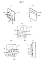
- Figs. 7(a) to 7(e) are diagrams showing a circuit substrate on which the semiconductor integrated circuit according to this embodiment is provided. As shown in Fig.7(a), contacts 12 are formed on a surface side of a circuit substrate 11. These contacts 12 are connected to the above-described external terminals P1 to P6. Further, as shown in Fig. 7(b), the semiconductor integrated circuit 1 is implemented or mounted on the back side of the circuit substrate 11.
- the circuit substrate 11 is in a substantially rectangular plate form.
- the circuit substrate 11 is provided with a notch portion 11 a and a hole portion 11 b. They are used for positioning the circuit substrate 11 when mounted on an ink-cartridge described below.
- a recess 12a may be provided on the surface of each of the contacts 12 provided on the circuit substrate 11. Providing the recess 12a, as shown in Fig. 7(e) improves the electric connection condition with a contact 29 provided on the ink cartridge described below.
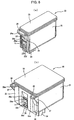
- Figs. 8(a) and (b) are diagrams for showing the circuit substrate shown in Fig. 7attached to an ink cartridge.
- Fig. 8(a) shows a case where the circuit substrate 11 is mounted on a black ink cartridge 20 accommodating black ink.
- the black ink cartridge 20 accommodates, in a container 21 formed as a substantially rectangular parallelepiped, a porous body, not shown, impregnated with black ink, and the top surface is sealed by a lid body 23.
- an ink supplying outlet 24 is formed at a position facing to an ink supplying needle when attached to a holder.
- an overhang portion 26 associated with a projection of a lever of the body is formed integrally at an upper edge of a vertical wall 25 at the side of the ink supplying outlet.
- the overhang portions 26 are formed on both sides of the wall 25 separately, and each has a rib 26a.
- a triangular rib 27 is formed between a bottom surface and the wall 25.
- the circuit substrate 11 is attached to the side where the ink supplying outlet of the horizontal wall 25 is formed.
- the circuit substrate 11 has a plurality of contacts on a surface facing the contacts of the body and has a memory element on the back surface.
- projections 25a and 25b and overhang portions 25c and 25d are formed on the horizontal wall 25 in order to position the circuit substrate 11.
- Fig. 8(b) shows a case where the circuit substrate 11 is attached to a color ink cartridge accommodating color ink.
- the color ink cartridge 30 accommodates, in a container 31 formed as a substantially rectangular parallelepiped, a porous body, not shown, impregnated with ink and sealed with a lid body 33 on the upper surface.
- Five ink accommodating portions accommodating five colors of color ink separately and respectively are sectionally formed inside of the container 31.
- an ink supplying outlet 34 is formed for each ink color at a position facing a respective ink supplying needle when attached to the holder.
- overhang portions 36 associated with a projection of a lever of the body is formed integrally at an upper edge of a vertical wall 35 at the side of the ink supplying outlet.
- the overhang portions 36 are formed on the both side of the wall 35 separately, and each has a rib 36a.
- a triangular rib 37 is formed between a bottom surface and the wall 35.
- the container 31 has a recess 39 in order to prevent a mis-insertion.
- a recess 38 is formed at a side of the horizontal wall 35 where an ink supplying outlet is formed such that it is positioned at the center of each cartridge 30 in the width direction, and the circuit substrate 11 is attached here.
- the circuit substrate 11 has a plurality of contacts on a surface facing to the contacts of the body and has a memory element on the back surface.
- projections 35a and 35b and overhang portions 35c and 35d are formed on the horizontal wall 35 in order to position the circuit substrate 11.
- Fig. 9 is a diagram showing an overview of an inkjet printer (inkjet recording device) to which an ink cartridge shown in Fig. 8 is attached.
- a holder 44 for accommodating each of the black ink cartridge 30 shown in Fig. 8(a) and the color ink cartridge 30 shown in Fig. 8(b) is formed in a carriage 43 connected to a driving motor 42 through a timing belt 41.
- a recording head 45 for receiving the supply of ink from each of the ink cartridges 20 and 30 is provided at a bottom surface position on the carriage 43.
- Ink supply needles 46 and 47 communicating with recording head 45 are provided vertically on the bottom surface of the carriage 43 such that they are positioned at the inner part of the device, that is on the side of the timing belt 41.
- Fig. 10 is a diagram showing the construction of the carriage shown in Fig. 9.
- levers 51 and 52 are mounted rotatably with respect to axes 49 and 50 as fulcrums at the upper edge of a vertical wall 48 closely facing to the ink supply needles 46 and 47 among vertical walls forming the holder 44.
- the wall 53 positioned on the side of free edges of the levers 51 and 52 has a slope portion where the bottom surface side is cut diagonally. Further, contact mechanisms 54 and 55 are provided on the vertical wall 48. The contact mechanisms 54 and 55 are connected to the above-described contacts provided on the circuit substrate 11 in a condition where the ink-cartridge is attached. Thus, ink-cartridge recording can be performed by using ink within the ink cartridge.
- a base platform 56 is mounted on the vertical wall 48 of the holder 44. Then, a circuit substrate 57 is mounted on the back surface of the base platform 56. The circuit substrate 57 is electrically connected with the contact mechanisms 54 and 55, resulting in that the circuit substrate 11 and the circuit substrate 57 provided in the ink cartridge are electrically connected.
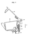
- Fig. 11 is a diagram showing the condition before the ink cartridge is attached to the holder
- Figs.12(a) to (c) are diagrams showing conditions where the ink cartridge is attached to the holder.
- Fig. 12(a) when the lever 51 is closed in a condition where the ink cartridge 20 is inserted to the holder 44, the ink cartridge 20 is pressed gradually in a direction of an arrow Y.
- the condition shown in Fig. 12(a) turns to the condition shown in Fig. 12(c), and the ink supply needle 46 is inserted into of the ink cartridge 20.
- Ink is supplied from the ink cartridge 20 in a condition where the ink supply needle 46 is inserted into of the ink cartridge 20 and the ink cartridge 20 is attached to the holder 44 completely, that is, in the condition shown in Fig. 12(c).
- an inkjet printer can read and write data freely to/from the semiconductor integrated circuit 1. More specifically, when the power supply of the printer is ON, "L” is applied to the external terminal P1, while “H” is applied when a read or write operation needs to be performed. It can simplify the logic and contribute to the reduction of the chip size.
- the remaining amount of ink cartridge can be always monitored.
Landscapes
- Read Only Memory (AREA)
- Ink Jet (AREA)
Abstract
Description
- Fig. 1
- is a circuit diagram showing one example of a discharge circuit within a semiconductor integrated circuit according to the present invention;
- Fig. 2
- is a functional block diagram for describing the internal construction of a semiconductor integrated circuit using the discharge circuit in Fig. 1;
- Fig. 3
- is a timing chart for describing a read-out operation on the semiconductor integration
- Fig. 4
- is a timing chart for describing a write-in operation on the semiconductor integrated
- Fig. 5
- is a timing chart showing an operation of each of the parts in Fig. 1;
- Fig. 6
- is a waveform diagram showing the state of charging/discharging of a parasitic capacity;
- Fig. 7
- is a diagram showing a circuit substrate on which the semiconductor integrated circuit shown in Fig. 1 is mounted;
- Fig. 8
- is a diagram showing the condition where the circuit substrate shown in Fig. 7 is mounted on an ink cartridge;
- Fig. 9
- is a diagram showing an overview of an inkjet printer to which the ink cartridge shown in Fig. 8 is attached;
- Fig. 10
- is a diagram showing the construction of a carriage shown in Fig. 9.
- Fig. 11
- is a diagram showing the condition before an ink cartridge is attached to a holder;
- Fig. 12
- is a diagram showing the condition where an ink cartridge is attached to a holder;
- Fig. 13
- is a block diagram showing one example of a conventional discharge circuit; and
- Fig. 14
- is a diagram for describing an operational example of the discharge circuit shown in Fig. 13.
Claims (7)
- A semiconductor integrated circuit, comprising charge means for charging a signal line corresponding to each 1 row in response to an input of a writing instruction for each bit of a memory cell arranged in n rows by m columns (where n and m are natural numbers and so forth) and charging a signal line corresponding to a next row after writing on all bits for one column is completed, the semiconductor integrated circuit performing writing on each 1 bit sequentially in each of bits for 1 column corresponding to the signal line charged by said charge means, and delay means for delaying an input of said writing instruction to said charge means for at least a time equivalent to a discharge time for said signal line.
- A semiconductor integrated circuit, comprising charge means for charging a signal line corresponding to each 1 row in response to an input of a writing instruction for each bit of a memory cell arranged in n rows by m columns and charging a signal line corresponding to a next row after writing on all bits for one column is completed, the semiconductor integrated circuit performing writing on each 1 bit sequentially in each of bits for 1 column corresponding to the signal line charged by said charge means, and suppressing means for suppressing a change in the address specifying a cell to be written within a predetermined time after completing the writing for 1 bit.
- A semiconductor integrated circuit according to claim 2, wherein said suppressing means is a delay circuit for delaying an input of said writing instruction to said charge means for at least a time equivalent to a discharge time for said signal line.
- A semiconductor integrated circuit, comprising charge means for charging a signal line corresponding to each 1 row in response to an input of a writing instruction for each bit of a memory cell arranged in n rows by m columns and charging a signal line corresponding to a next row after writing on all bits for one column is completed, the semiconductor integrated circuit performing writing on each 1 bit sequentially in each of bits for 1 column corresponding to the signal line charged by said charge means, and delay means for making different the timing for completing writing for 1 bit and the timing for changing the address specifying a cell to be written for a time equivalent to a time for charging at least said signal line.
- A semiconductor integrated circuit according to any one of claims 1 to 4, wherein said charge means comprises a counter for starting an count operation in response to an input of said writing instruction, a column decoder for decoding the count value of said counter, a switching element for charging said signal line by connecting a predetermined power supply to said signal line after being turned ON depending on the decoding result by said decoder, and a row decoder for specifying each 1 bit sequentially for 1 row of bits corresponding to the signal line charged when said switching element is turned ON.
- An ink cartridge having the semiconductor integrated circuit according to any one of claims 1 to 5, for storing at least a remaining amount of ink on said memory cell.
- An inkjet recording device having an ink cartridge according to claim 6 for printing desired image information by using ink supplied from the ink cartridge.
Applications Claiming Priority (3)
| Application Number | Priority Date | Filing Date | Title |
|---|---|---|---|
| JP28324599 | 1999-10-04 | ||
| JP28324599 | 1999-10-04 | ||
| PCT/JP2000/006935 WO2001026115A1 (en) | 1999-10-04 | 2000-10-04 | Semiconductor integrated circuit, ink cartridge having this semiconductor integrated circuit, and ink jet recording device mounted with this ink cartridge |
Publications (2)
| Publication Number | Publication Date |
|---|---|
| EP1156490A1 true EP1156490A1 (en) | 2001-11-21 |
| EP1156490A4 EP1156490A4 (en) | 2002-10-31 |
Family
ID=17662977
Family Applications (1)
| Application Number | Title | Priority Date | Filing Date |
|---|---|---|---|
| EP20000964674 Withdrawn EP1156490A4 (en) | 1999-10-04 | 2000-10-04 | INTEGRATED SEMICONDUCTOR CIRCUIT, INK CARTRIDGE COMPRISING THIS INTEGRATED SEMICONDUCTOR CIRCUIT, AND INK JET RECORDING DEVICE WITH THIS INK CARTRIDGE |
Country Status (7)
| Country | Link |
|---|---|
| US (1) | US6487123B1 (en) |
| EP (1) | EP1156490A4 (en) |
| JP (1) | JP4469531B2 (en) |
| KR (1) | KR20010080651A (en) |
| CN (1) | CN1338106A (en) |
| TW (1) | TW536706B (en) |
| WO (1) | WO2001026115A1 (en) |
Cited By (2)
| Publication number | Priority date | Publication date | Assignee | Title |
|---|---|---|---|---|
| FR2843480A1 (en) * | 2002-08-12 | 2004-02-13 | Seiko Epson Corp | CARTRIDGE AND RECORDING APPARATUS |
| US10259230B2 (en) | 2005-12-26 | 2019-04-16 | Seiko Epson Corporation | Printing material container, and board mounted on printing material container |
Families Citing this family (4)
| Publication number | Priority date | Publication date | Assignee | Title |
|---|---|---|---|---|
| DE10225953A1 (en) * | 2002-06-11 | 2003-12-24 | Schunk Kohlenstofftechnik Gmbh | Method for producing a carbon body having a honeycomb structure |
| JP2005092963A (en) * | 2003-09-16 | 2005-04-07 | Renesas Technology Corp | Nonvolatile memory |
| PT3710262T (en) | 2019-02-06 | 2021-12-31 | Hewlett Packard Development Co | Accessing registers of fluid ejection devices |
| US11351775B2 (en) * | 2019-02-06 | 2022-06-07 | Hewlett-Packard Development Company, L.P. | Integrated circuits including customization bits |
Family Cites Families (16)
| Publication number | Priority date | Publication date | Assignee | Title |
|---|---|---|---|---|
| JPS61271688A (en) * | 1985-05-27 | 1986-12-01 | Matsushita Electric Ind Co Ltd | Bipolar memory |
| JPH0715799B2 (en) * | 1987-06-30 | 1995-02-22 | 日本電気株式会社 | Semiconductor memory device |
| US5229963A (en) * | 1988-09-21 | 1993-07-20 | Kabushiki Kaisha Toshiba | Semiconductor nonvolatile memory device for controlling the potentials on bit lines |
| JPH0814996B2 (en) * | 1989-06-27 | 1996-02-14 | 株式会社東芝 | Semiconductor memory device |
| US5732035A (en) * | 1990-06-14 | 1998-03-24 | Creative Integrated Systems, Inc. | Very large scale integrated planar read only memory |
| KR930006622B1 (en) * | 1990-09-04 | 1993-07-21 | 삼성전자 주식회사 | Semiconductor memory |
| JPH05301349A (en) | 1992-04-24 | 1993-11-16 | Canon Inc | Printer |
| JP2839995B2 (en) * | 1992-10-14 | 1998-12-24 | キヤノン株式会社 | Recording device |
| JPH06162784A (en) * | 1992-11-17 | 1994-06-10 | Oki Micro Design Miyazaki:Kk | Semiconductor integrated circuit device |
| JP3526894B2 (en) * | 1993-01-12 | 2004-05-17 | 株式会社ルネサステクノロジ | Nonvolatile semiconductor memory device |
| KR970017662A (en) * | 1995-09-04 | 1997-04-30 | 김광호 | Data Collision Avoidance Circuit in SRAM |
| JPH09153288A (en) * | 1995-11-30 | 1997-06-10 | Mitsubishi Electric Corp | Semiconductor memory device |
| JPH09265791A (en) * | 1996-03-28 | 1997-10-07 | Nec Corp | Semiconductor memory |
| JPH1069793A (en) * | 1996-08-29 | 1998-03-10 | Nec Kyushu Ltd | Semiconductor memory device |
| JP3497770B2 (en) * | 1999-05-20 | 2004-02-16 | 株式会社 沖マイクロデザイン | Semiconductor storage device |
| JP3599317B2 (en) * | 1999-05-25 | 2004-12-08 | シャープ株式会社 | Semiconductor memory |
-
2000
- 2000-10-04 JP JP2001528990A patent/JP4469531B2/en not_active Expired - Lifetime
- 2000-10-04 US US09/857,451 patent/US6487123B1/en not_active Expired - Fee Related
- 2000-10-04 WO PCT/JP2000/006935 patent/WO2001026115A1/en not_active Ceased
- 2000-10-04 TW TW089120689A patent/TW536706B/en not_active IP Right Cessation
- 2000-10-04 EP EP20000964674 patent/EP1156490A4/en not_active Withdrawn
- 2000-10-04 CN CN00803047A patent/CN1338106A/en active Pending
- 2000-10-04 KR KR1020017006842A patent/KR20010080651A/en not_active Ceased
Cited By (11)
| Publication number | Priority date | Publication date | Assignee | Title |
|---|---|---|---|---|
| FR2843480A1 (en) * | 2002-08-12 | 2004-02-13 | Seiko Epson Corp | CARTRIDGE AND RECORDING APPARATUS |
| EP1389528A1 (en) * | 2002-08-12 | 2004-02-18 | Seiko Epson Corporation | Cartridge and recording apparatus |
| GB2393937B (en) * | 2002-08-12 | 2005-03-16 | Seiko Epson Corp | Cartridge and recording apparatus |
| US6984012B2 (en) | 2002-08-12 | 2006-01-10 | Seiko Epson Corporation | Cartridge and recording apparatus |
| AU2003231707B2 (en) * | 2002-08-12 | 2007-06-07 | Seiko Epson Corporation | Cartridge and Recording Apparatus |
| US10259230B2 (en) | 2005-12-26 | 2019-04-16 | Seiko Epson Corporation | Printing material container, and board mounted on printing material container |
| US10625510B2 (en) | 2005-12-26 | 2020-04-21 | Seiko Epson Corporation | Printing material container, and board mounted on printing material container |
| US10836173B2 (en) | 2005-12-26 | 2020-11-17 | Seiko Epson Corporation | Printing material container, and board mounted on printing material container |
| US11279138B2 (en) | 2005-12-26 | 2022-03-22 | Seiko Epson Corporation | Printing material container, and board mounted on printing material container |
| US11667126B2 (en) | 2005-12-26 | 2023-06-06 | Seiko Epson Corporation | Printing material container, and board mounted on printing material container |
| US11945231B2 (en) | 2005-12-26 | 2024-04-02 | Seiko Epson Corporation | Printing material container, and board mounted on printing material container |
Also Published As
| Publication number | Publication date |
|---|---|
| TW536706B (en) | 2003-06-11 |
| WO2001026115A1 (en) | 2001-04-12 |
| EP1156490A4 (en) | 2002-10-31 |
| KR20010080651A (en) | 2001-08-22 |
| US6487123B1 (en) | 2002-11-26 |
| JP4469531B2 (en) | 2010-05-26 |
| CN1338106A (en) | 2002-02-27 |
Similar Documents
| Publication | Publication Date | Title |
|---|---|---|
| US6655768B1 (en) | Semiconductor integrated circuit, ink cartridge, and inkjet recording device | |
| CN100383894C (en) | Integrated circuit and method of operating an integrated circuit | |
| US20020034101A1 (en) | Nonvolatile semiconductor storage device capable of correctly reading selected memory cell and read method therefor | |
| US6594185B1 (en) | Write-inhibit circuit, semiconductor integrated circuit using the same, ink cartridge including the semiconductor integrated circuit, and ink-jet recording apparatus | |
| EP1156490A1 (en) | Semiconductor integrated circuit, ink cartridge having this semiconductor integrated circuit, and ink jet recording device mounted with this ink cartridge | |
| US11370223B2 (en) | Accessing memory units in a memory bank | |
| JPWO2001026116A1 (en) | Write-protect circuit, semiconductor integrated circuit using the same, ink cartridge having the semiconductor integrated circuit, and ink-jet recording apparatus | |
| JPWO2001026115A1 (en) | Semiconductor integrated circuit, ink cartridge having the semiconductor integrated circuit, and ink jet recording device equipped with the ink cartridge | |
| US7337282B2 (en) | Memory system and process for controlling a memory component to achieve different kinds of memory characteristics on one and the same memory component | |
| JP3582471B2 (en) | Semiconductor integrated circuit, ink cartridge having this semiconductor integrated circuit, and ink jet recording apparatus equipped with this ink cartridge | |
| EP1063653B1 (en) | Nonvolatile memory device, in particular of flash type | |
| CN1862705B (en) | Nonvolatile semiconductor memory and method of writing data into the memory | |
| JP2988382B2 (en) | Semiconductor storage device | |
| US6940755B2 (en) | Semiconductor with an improved read device and operational mode associated therewith | |
| JPH07307095A (en) | Electrically erasable semiconductor memory provided with counter |
Legal Events
| Date | Code | Title | Description |
|---|---|---|---|
| PUAI | Public reference made under article 153(3) epc to a published international application that has entered the european phase |
Free format text: ORIGINAL CODE: 0009012 |
|
| 17P | Request for examination filed |
Effective date: 20010704 |
|
| AK | Designated contracting states |
Kind code of ref document: A1 Designated state(s): AT BE CH CY DE DK ES FI FR GB GR IE IT LI LU MC NL PT SE |
|
| AX | Request for extension of the european patent |
Free format text: AL;LT;LV;MK;RO;SI |
|
| A4 | Supplementary search report drawn up and despatched | ||
| AK | Designated contracting states |
Kind code of ref document: A4 Designated state(s): AT BE CH CY DE DK ES FI FR GB GR IE IT LI LU MC NL PT SE |
|
| RIC1 | Information provided on ipc code assigned before grant |
Free format text: 7G 11C 17/00 A, 7B 41J 2/175 B, 7G 11C 7/22 B, 7G 11C 16/32 B |
|
| A4 | Supplementary search report drawn up and despatched |
Effective date: 20021031 |
|
| 17Q | First examination report despatched |
Effective date: 20030212 |
|
| STAA | Information on the status of an ep patent application or granted ep patent |
Free format text: STATUS: THE APPLICATION IS DEEMED TO BE WITHDRAWN |
|
| 18D | Application deemed to be withdrawn |
Effective date: 20030822 |
|
| RBV | Designated contracting states (corrected) |
Designated state(s): DE ES FR GB IT |