EP1156311A1 - Photodetector array and optical branching filter using the array - Google Patents
Photodetector array and optical branching filter using the array Download PDFInfo
- Publication number
- EP1156311A1 EP1156311A1 EP00964677A EP00964677A EP1156311A1 EP 1156311 A1 EP1156311 A1 EP 1156311A1 EP 00964677 A EP00964677 A EP 00964677A EP 00964677 A EP00964677 A EP 00964677A EP 1156311 A1 EP1156311 A1 EP 1156311A1
- Authority
- EP
- European Patent Office
- Prior art keywords
- light
- receiving element
- receiving
- element array
- elements
- Prior art date
- Legal status (The legal status is an assumption and is not a legal conclusion. Google has not performed a legal analysis and makes no representation as to the accuracy of the status listed.)
- Withdrawn
Links
- 230000003287 optical effect Effects 0.000 title description 11
- 238000012544 monitoring process Methods 0.000 claims abstract description 75
- 239000000758 substrate Substances 0.000 claims description 8
- 238000000034 method Methods 0.000 claims description 3
- 239000004065 semiconductor Substances 0.000 claims 14
- 239000000463 material Substances 0.000 claims 1
- 230000003247 decreasing effect Effects 0.000 description 9
- 230000003595 spectral effect Effects 0.000 description 8
- 238000001228 spectrum Methods 0.000 description 6
- 238000009792 diffusion process Methods 0.000 description 5
- 239000000835 fiber Substances 0.000 description 5
- 239000002184 metal Substances 0.000 description 4
- 239000013307 optical fiber Substances 0.000 description 4
- 229910000530 Gallium indium arsenide Inorganic materials 0.000 description 3
- 238000004891 communication Methods 0.000 description 3
- 230000005856 abnormality Effects 0.000 description 2
- 230000005540 biological transmission Effects 0.000 description 2
- 239000000969 carrier Substances 0.000 description 2
- 239000006185 dispersion Substances 0.000 description 2
- 230000000694 effects Effects 0.000 description 2
- 238000003491 array Methods 0.000 description 1
- 230000008878 coupling Effects 0.000 description 1
- 238000010168 coupling process Methods 0.000 description 1
- 238000005859 coupling reaction Methods 0.000 description 1
- 230000031700 light absorption Effects 0.000 description 1
- 238000000926 separation method Methods 0.000 description 1
Images






Classifications
-
- G—PHYSICS
- G01—MEASURING; TESTING
- G01J—MEASUREMENT OF INTENSITY, VELOCITY, SPECTRAL CONTENT, POLARISATION, PHASE OR PULSE CHARACTERISTICS OF INFRARED, VISIBLE OR ULTRAVIOLET LIGHT; COLORIMETRY; RADIATION PYROMETRY
- G01J3/00—Spectrometry; Spectrophotometry; Monochromators; Measuring colours
- G01J3/28—Investigating the spectrum
- G01J3/30—Measuring the intensity of spectral lines directly on the spectrum itself
- G01J3/36—Investigating two or more bands of a spectrum by separate detectors
-
- G—PHYSICS
- G01—MEASURING; TESTING
- G01J—MEASUREMENT OF INTENSITY, VELOCITY, SPECTRAL CONTENT, POLARISATION, PHASE OR PULSE CHARACTERISTICS OF INFRARED, VISIBLE OR ULTRAVIOLET LIGHT; COLORIMETRY; RADIATION PYROMETRY
- G01J3/00—Spectrometry; Spectrophotometry; Monochromators; Measuring colours
- G01J3/28—Investigating the spectrum
- G01J3/2803—Investigating the spectrum using photoelectric array detector
-
- H—ELECTRICITY
- H04—ELECTRIC COMMUNICATION TECHNIQUE
- H04B—TRANSMISSION
- H04B10/00—Transmission systems employing electromagnetic waves other than radio-waves, e.g. infrared, visible or ultraviolet light, or employing corpuscular radiation, e.g. quantum communication
- H04B10/07—Arrangements for monitoring or testing transmission systems; Arrangements for fault measurement of transmission systems
- H04B10/075—Arrangements for monitoring or testing transmission systems; Arrangements for fault measurement of transmission systems using an in-service signal
- H04B10/079—Arrangements for monitoring or testing transmission systems; Arrangements for fault measurement of transmission systems using an in-service signal using measurements of the data signal
- H04B10/0795—Performance monitoring; Measurement of transmission parameters
- H04B10/07953—Monitoring or measuring OSNR, BER or Q
-
- H—ELECTRICITY
- H10—SEMICONDUCTOR DEVICES; ELECTRIC SOLID-STATE DEVICES NOT OTHERWISE PROVIDED FOR
- H10F—INORGANIC SEMICONDUCTOR DEVICES SENSITIVE TO INFRARED RADIATION, LIGHT, ELECTROMAGNETIC RADIATION OF SHORTER WAVELENGTH OR CORPUSCULAR RADIATION
- H10F30/00—Individual radiation-sensitive semiconductor devices in which radiation controls the flow of current through the devices, e.g. photodetectors
- H10F30/20—Individual radiation-sensitive semiconductor devices in which radiation controls the flow of current through the devices, e.g. photodetectors the devices having potential barriers, e.g. phototransistors
- H10F30/21—Individual radiation-sensitive semiconductor devices in which radiation controls the flow of current through the devices, e.g. photodetectors the devices having potential barriers, e.g. phototransistors the devices being sensitive to infrared, visible or ultraviolet radiation
- H10F30/22—Individual radiation-sensitive semiconductor devices in which radiation controls the flow of current through the devices, e.g. photodetectors the devices having potential barriers, e.g. phototransistors the devices being sensitive to infrared, visible or ultraviolet radiation the devices having only one potential barrier, e.g. photodiodes
- H10F30/223—Individual radiation-sensitive semiconductor devices in which radiation controls the flow of current through the devices, e.g. photodetectors the devices having potential barriers, e.g. phototransistors the devices being sensitive to infrared, visible or ultraviolet radiation the devices having only one potential barrier, e.g. photodiodes the potential barrier being a PIN barrier
-
- H—ELECTRICITY
- H10—SEMICONDUCTOR DEVICES; ELECTRIC SOLID-STATE DEVICES NOT OTHERWISE PROVIDED FOR
- H10F—INORGANIC SEMICONDUCTOR DEVICES SENSITIVE TO INFRARED RADIATION, LIGHT, ELECTROMAGNETIC RADIATION OF SHORTER WAVELENGTH OR CORPUSCULAR RADIATION
- H10F39/00—Integrated devices, or assemblies of multiple devices, comprising at least one element covered by group H10F30/00, e.g. radiation detectors comprising photodiode arrays
- H10F39/10—Integrated devices
- H10F39/107—Integrated devices having multiple elements covered by H10F30/00 in a repetitive configuration, e.g. radiation detectors comprising photodiode arrays
-
- G—PHYSICS
- G02—OPTICS
- G02B—OPTICAL ELEMENTS, SYSTEMS OR APPARATUS
- G02B6/00—Light guides; Structural details of arrangements comprising light guides and other optical elements, e.g. couplings
- G02B6/24—Coupling light guides
- G02B6/26—Optical coupling means
- G02B6/28—Optical coupling means having data bus means, i.e. plural waveguides interconnected and providing an inherently bidirectional system by mixing and splitting signals
- G02B6/293—Optical coupling means having data bus means, i.e. plural waveguides interconnected and providing an inherently bidirectional system by mixing and splitting signals with wavelength selective means
- G02B6/29304—Optical coupling means having data bus means, i.e. plural waveguides interconnected and providing an inherently bidirectional system by mixing and splitting signals with wavelength selective means operating by diffraction, e.g. grating
- G02B6/29305—Optical coupling means having data bus means, i.e. plural waveguides interconnected and providing an inherently bidirectional system by mixing and splitting signals with wavelength selective means operating by diffraction, e.g. grating as bulk element, i.e. free space arrangement external to a light guide
- G02B6/29307—Optical coupling means having data bus means, i.e. plural waveguides interconnected and providing an inherently bidirectional system by mixing and splitting signals with wavelength selective means operating by diffraction, e.g. grating as bulk element, i.e. free space arrangement external to a light guide components assembled in or forming a solid transparent unitary block, e.g. for facilitating component alignment
-
- G—PHYSICS
- G02—OPTICS
- G02B—OPTICAL ELEMENTS, SYSTEMS OR APPARATUS
- G02B6/00—Light guides; Structural details of arrangements comprising light guides and other optical elements, e.g. couplings
- G02B6/24—Coupling light guides
- G02B6/26—Optical coupling means
- G02B6/28—Optical coupling means having data bus means, i.e. plural waveguides interconnected and providing an inherently bidirectional system by mixing and splitting signals
- G02B6/293—Optical coupling means having data bus means, i.e. plural waveguides interconnected and providing an inherently bidirectional system by mixing and splitting signals with wavelength selective means
- G02B6/29304—Optical coupling means having data bus means, i.e. plural waveguides interconnected and providing an inherently bidirectional system by mixing and splitting signals with wavelength selective means operating by diffraction, e.g. grating
- G02B6/29305—Optical coupling means having data bus means, i.e. plural waveguides interconnected and providing an inherently bidirectional system by mixing and splitting signals with wavelength selective means operating by diffraction, e.g. grating as bulk element, i.e. free space arrangement external to a light guide
- G02B6/2931—Diffractive element operating in reflection
Definitions
- the present invention relates to an optical demultiplexer for monitoring the spectrum of wavelength multiplexed light, and further relates to a light-receiving element array used in a photodetector of the optical demultiplexer.
- an optical demultiplexer is used as a device for demultiplexing the received wavelength multiplexed light beam every wavelength into a plurality of light beams each thereof having one wavelength, and monitoring the spectrum of each of the demultiplexed light beams.
- the spectrum of each light beam may be detected when each light-receiving element in the array is arranged correspondingly with respect to each light beam.
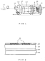
- the optical demultiplexer comprises components such as an input optical fiber 2, a collimator lens 4, a diffraction grating 6, and a photodetector 8. These components are accommodated in three tubular members which are fitted to each other.
- the input optical fiber 2 consisted of a single core is fixedly coupled to a window 12 for fixing the fiber by means of a fiber coupling member 14, the window 12 being an end face of a transparent tube 10 for accommodating the fiber.
- the collimator lens 4 are fixed to an end of an intermediate tube 16.
- the diffraction grating 6 is fixed to an window 20, the window 20 being an end face of a tube 18 for accommodating the diffraction grating.
- the tubes 10 and 18 are fitted to both ends of the intermediate tube 16 so as to be movable in the direction of light axis and rotatable around the light axis for active alignment.
- the light beam from the input optical fiber 2 is guided into the optical demultiplexer. At this time, the light beam is diverged due to the numerical aperture of the fiber 2.
- the divergent beam reaches to the collimator lens 4 and is converged into parallel light beam by the collimator lens.
- the parallel light beam reaches to the diffraction grating 6 and is demodulated (or isolated) into a plurality light beams every wavelength by the wavelength dispersion characteristic of the diffraction grating 6.
- the demodulated light beams are converted into convergent light beams, respectively, by the collimator lens 4. These convergent light beams impinge upon the window 12 which is positioned at a focal point of the collimator lens, and are arranged in one line on the window.
- the photodetection for each light beam may be possible, when the photodetector 8 is secured to the window 20 in such a manner that each light beam impinges correspondingly upon each light-receiving element of the photodet
- a diffusion-type or mesa-type of light-receiving element array for the device.
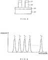
- the structure of a diffusion-type light-receiving element array is shown in Fig.2.
- An n-type InP layer 24, an i-type InGaAs layer (i.e., a light-absorbing layer) 26, and an n-type InP layer (i.e., a window layer) 28 are stacked in this order on an n-type InP substrate 22.
- Zn is diffused into the n-type InP layer 28 to form p-type regions 30 in order to fabricate pin-photodiodes.
- One pin-photodiode constructs one light-emitting element.
- the diffusion is isotropic so that Zn diffusion also proceeds in a lateral direction.
- this diffusion-type light-receiving element array therefore, it is limited to decrease the interval of elements, e.g., the limit value is about 50 ⁇ m.
- a mesa-type light-emitting element array is shown in Fig.3.
- An n-type InP layer 24, an i-type InGaAs layer 26, and a p-type InP layer 27 are stacked in this order on an n-type InP substrate 22. Both the InGaAs layer 26 and InP layer 27 are etched away to isolate the elements in order to fabricate pin-photodiodes.
- One pin-photodiode constructs one light-receiving element.
- the mesa-type light-emitting element array has no limitation for the interval of elements, so that the array pitch of the elements may be further decreased.
- the expansion of spectral width and the shift of wavelength may be occurred, principally in a fiber amplifier of the optical communication system, the spread of spectral width and the shift of wavelength being referred to as noise hereinafter.
- noise the spread of spectral width and the shift of wavelength being referred to as noise hereinafter.
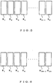
- the following problem is caused. That is, when N-channel light is monitored, in which light beams L 1 , L 2 , L 3 , ⁇ each having a narrower spectral width are multiplexed as shown in Fig.4, the strict separation between a signal and a noise in each channel is impossible for the case that light-receiving elements R 1 , R 2 , R 3 , ⁇ , R N for monitoring signals are simply arranged in one line as shown in Fig.5.
- the light-receiving element array consisting of light-receiving elements R 1 , R 2 , R 3 , ⁇ arrayed in one line as described with reference to Fig.5 may be used, but the alignment between the demultiplexed light beams L 1 , L 2 , L 3 , ⁇ and the light-receiving elements R 1 , R 2 , R 3 , ⁇ is very difficult.
- the carriers caused in one light-receiving element by light absorption are laterally diffused and are transferred to the adjacent light-emitting elements. Therefore, a current flows in the light-emitting elements to which light is not incident upon, resulting in a crosstalk. As a result, the characteristic of the light-emitting element array may be deteriorated.
- a first aspect of the present invention provides a light demultiplexer in which a signal and a noise in each channel may be distinctly separated, and a light-receiving element array used for a photodetector of the light demultiplexer.
- the strength of a signal in one channel is monitored by one light-receiving element for monitoring a signal, and at the same time, a noise is monitored by at least one light-receiving element for monitoring a noise which is adjacent to said one light-receiving element for monitoring a signal.
- N-channel of signals and noises may be detected by means of about 2N light-receiving elements arrayed in a straight line.
- the light-receiving elements for monitoring signals and the light-receiving elements for monitoring noises are alternately arrayed. A signal and noise in each wavelength are detected by adjacent light-receiving elements to monitor the demultiplexed light beams. According to this, if the output from the element for monitoring a signal is decreased and the output from the elements for monitoring a noise is increased, then it is appreciated that any abnormality is caused for the spectrum of demultiplexed light beam. As examples of the abnormality, the peak position of spectrum is shifted to a high wavelength or low wavelength side, the spectral width of spectrum is spread, and the like are estimated.
- the output from the element for monitoring a signal is not varied and the output from the element for monitoring a noise is increased, then it is appreciated that the noise in a corresponding channel is increased.
- the shift of the spectral peak and the variation of a noise may be monitored by alternately arraying the element for monitoring a signal and the element for monitoring a noise.
- a second aspect of the present invention provides a light demultiplexer in which the alignment between demultiplexed light beams and light-receiving elements may be precisely implemented as well as the resolution of a light demultiplexer may be improved, and a light-receiving element array used for a photodetector of the light demultiplexer. Furthermore, a method for aligning light-receiving elements and demultiplexed light beams.
- one demultiplexed light beam is not received only by one light-receiving element but a plurality of light-receiving elements to compare the output signals from these elements, so that the position of demultiplexed light beams may be aligned with respect to the plurality of the elements.
- first light-receiving elements arrayed in a predetermined pitch and in the same direction as that of the arrangement of the demultiplexed light beams and a plurality of second light-receiving elements arrayed in the same pitch as the predetermined pitch and in the same direction as that of the arrangement of the demultiplexed light beams are arrayed with one-half pitch shifted in an array direction.
- the output signals from three light-receiving elements which are adjacent to each other in a direction perpendicular to the array direction of the first and second light-receiving elements are used, and the center of a demultiplexed light beam is aligned to the contact point of the three adjacent elements.
- the alignment between a light beam and a light-receiving element may be precisely implemented. Also, the resolution of the light demultiplexer may be improved such as two times by the arrangement of the light-receiving element array.
- a third aspect of the present invention provides a light demultiplexer in which a crosstalk between adjacent light-receiving elements may be decreased, and a light-receiving element array used for a photodetector of the light demultiplexer.
- a light-receiving element array for receiving light beams demultiplexed every wavelength from a wavelength multiplexed light beam and arranged in a straight line comprises a plurality of light-receiving elements for monitoring signals, and a plurality of electrode shorted light-receiving elements, wherein the light-receiving elements for monitoring signals and the electrode shorted light-receiving elements are alternately arrayed in a straight line the direction thereof is the same as that of the arrangement of the demultiplexed light beams.
- a crosstalk between the light-receiving elements may be decreased.
- the crosstalk may be effectively decreased by providing a light shielding film on the light-receiving surface of the electrode shorted light-receiving element. Also, it may be prevented the light-receiving element array becomes large in order to decrease a crosstalk by making the element area of the electrode shorted light-receiving element smaller than that of the light-receiving element for monitoring a signal.
- the present embodiment is directed to a light demultiplexer in which a signal and a noise in the wavelength multiplexed light are distinctly separated, and a light-receiving element array used for a photodetector of the light demultiplexer.
- the structure of a light demultiplexer according to the present embodiment is substantially the same as that shown in Fig.1 except a photodetector.
- a light-emitting element array according to the present embodiment is used as the photodetector 8.
- An example of the light-receiving element array is shown in Fig.6.
- N channels N is an integer of 2 or more
- odd-numbered light-receiving elements for monitoring signals R 1 , R 3 , ⁇ , R 2N-1 and even-numbered light-receiving elements R 2 , R 4 , ⁇ , R 2N for monitoring noises are alternately arrayed.
- the total number of light-receiving elements is two times the number of demultiplexed light beams, i.e. 2N.
- the element for monitoring a signal monitors the strength of a signal
- the element for monitoring a noise monitors the strength of a noise.
- the signal For a first channel of demultiplexed light beam, the signal is monitored by the element R 1 , and the noise by the element R 2 .
- the signal For a second channel of demultiplexed light beams, the signal is monitored by the element R 3 , and the noise by the elements R 2 , R 4 .
- the signal For a last channel of demultiplexed light beam, the signal is monitored by the element R 2N-1 , and the noise by the elements R 2N-2 , R 2N .
- the diffusion-type light-receiving element array as described with reference to Fig.2 may be used by way of example.
- Zn diffusion laterally proceeds in the element, so that the interval of elements may not be narrower than 50 ⁇ m, i.e. there is a limitation for the interval of elements.
- Fig.7 shows a plan view of a chip 30 formed by the diffusion-type light-receiving element array.
- the elements for monitoring signals R 1 , R 3 , ⁇ , R 2N-1 and the elements for monitoring noises R 2 , R 4 , ⁇ , R 2N are connected to corresponding bonding pads 36 through a wiring 34, respectively.
- the interval p 1 of elements is required to be larger than 50 ⁇ m.
- the mesa-type light-receiving as described in Fig.3 may also be used for a light-receiving element array.
- the mesa-type light-receiving element array may prevent the limitation of the interval of elements due to the lateral diffusion, which is the problem caused in the structure of the diffusion-type one as described above.
- a high-density light-receiving element array such as 25 ⁇ m or 10 ⁇ m interval, may be provided.
- Fig.8 shows a plan view of a chip 32 formed by the mesa-type light-receiving element array.
- the interval of elements may be small such as 10 ⁇ m.
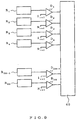
- Fig.9 shows a circuitry for detecting N channels of signal and noises which have been separated.
- This detecting circuitry comprises signal monitoring differential amplifiers D 1 , D 3 , ⁇ , D 2N-1 to one input terminal thereof the element for monitoring a signal is connected, noise monitoring differential amplifiers D 2 , D 4 , ⁇ , D 2N to one input terminal thereof the element for monitoring a noise is connected, and a signal/noise monitoring output circuit 40.
- a reference level I ref is connected to the other input terminal of the signal monitoring differential amplifiers D 1 , D 3 , ⁇ , D 2N-1
- a reference level N ref is connected to the other input terminal of the noise monitoring differential amplifiers D 2 , D 4 , ⁇ , D 2N .
- the signals and noises are monitored based on those reference levels.
- the wavelength multiplexed light beam from the input optical fiber 2 is converted into a parallel light beam by the collimator lens, and the parallel light beam reaches to the diffraction grating 6.
- the parallel light beam is separated every wavelength into a plurality of demultiplexed beams based on the wavelength dispersion characteristic of the diffraction grating 6.
- the demultiplexed light beams are converted into convergent light beams, respectively, by the collimator lens 4. These convergent light beams impinge upon the photodetector 16 which is positioned at a focal point of the collimator lens 4.
- Fig.10 shows that all of the demultiplexed light beams impinge upon the light-receiving elements for monitoring the signals without causing the spread of spectral width and the shift of wavelength.
- each differential amplifier in Fig.9 does not output a signal, so that the signal/noise monitoring output circuit 40 does not detect the spread of spectral width and the shift of wavelength.
- Fig.11 shows that the peak wavelength of the demultiplexed light beam L 1 is shifted from the normal value.
- the detecting output of the light-receiving element R 1 for monitoring a signal is decreased, and the detecting output of the light-receiving element R 2 for monitoring a noise is increased.
- the differential amplifier D 1 subtracts the reference level I ref from the signal output of the element R 1 to output it as a signal. Also, the differential amplifier D 2 subtracts the reference level N ref from the noise output of the element R 2 to output it as a noise.
- the signal/noise monitoring output circuit 40 may detect the shift of the peak position of the demultiplexed light beam L 1 , i.e. the shift of wavelength from the outputs of the differential amplifier D 1 , D 2 .
- the odd-numbered elements are ones for monitoring signals and the even-numbered elements are ones for monitoring noises, but it is also possible that the even-numbered elements are ones for monitoring signals and the odd-numbered elements are ones for monitoring noises.
- the array including 2N elements is illustrated for simplicity in Fig.6, but it may be possible to use only 2N elements in the array including more than 2N elements.
- (2N+1) elements are used to arrange the elements for monitoring noises at both ends of the light-receiving element array, then it is preferably performed to monitor noises at first and last channels.
- an additional element for monitoring a noise is necessarily arranged on the left side of the element R 1 for monitoring a signal, so that a noise monitoring for the first channel of demultiplexed light beam L 1 may be implemented by means of the additional element and element R 2 for monitoring noises.
- the noises between channels may be monitored by (N-1) elements for monitoring noises, so that light-receiving element array may be structured by (2N-1) elements.
- the present embodiment is directed to a light demultiplexer in which the alignment between demultiplexed light beams and light-receiving elements may be precisely implemented as well as the resolution thereof may be improved, and a light-receiving element array used for a photodetector of the light demultiplexer.
- a light demultiplexer is substantially the same as that shown in Fig.1 except a photodetector.
- a light-emitting element array according to the present embodiment is used.
- the light-receiving element array will now be described with reference to Fig.12.
- a light-receiving array chip 48 constructed by two rows of element arrays is illustrated.
- One row of elements are designated by odd-numbered elements R 1 , R 3 , R 5 , R 7 , R 9 , ⁇ , the other row of elements by even-numbered elements R 2 , R 4 , R 6 , R 8 , ⁇ .
- the array pitch in one row of elements is the same as that of the other row of elements, and these two rows of elements are arrayed with one-half pitch shifted.
- the elements R 1 , R 3 , R 5 , R 7 , R 9 , ⁇ in one row are connected to boding pads 40 arranged opposing to the elements, through a wiring 42, respectively, and the elements R 2 , R 4 , R 6 , R 8 , ⁇ in the other row are connected to bonding pads 44 arranged opposing to the elements through a wiring 46, respectively.
- boding pads are arrayed in one row on one side of the two rows of elements, i.e. near the side edge of the light-receiving element array chip.
- Fig.13 shows the light-receiving element array consisting of two rows elements and the demultiplexed light beams (only the light beams L 1 , L 2 and L N are designated in the figure).
- each of the demultiplexed light beams impinges upon three light-receiving elements which are adjacent to each other in a direction perpendicular to an array direction of the two rows of elements.
- the output signals (current or voltage) from these three adjacent elements are monitored.
- the demultiplexed light beam L 1 are monitored by the elements R 2 R 3 , R 4 and the light beam L 2 by the element R 6 , R 7 , R 8 .
- the alignment of the demultiplexed light beams with respect to the light-receiving element array may be implemented at a high precision. For example, in order to align the center of the light beam L 1 is aligned with respect to a contact point S of three adjacent elements R 2 , R 3 and R 4 , respective amounts of light detected by the elements R 2 and R 4 are caused to be the same, and the sum of the amounts of light detected by the elements R 2 and R 4 is caused to be identical with the amount of light detected by the element R 3 .
- the center point of the demultiplexed light beam L 2 is designated to be shifted from the contact point S of the elements R 6 , R 7 , R 8 .
- the respective amounts of light detected by the elements R 6 and R 8 are different, and the sum of amounts of light detected by the elements R 6 and R 8 is the same as the amount of light detected by the element R 7 , so that it is appreciated that the light beam L 2 is shifted in an array direction of elements with respect to the contact point S .
- the resolution of the light-receiving element array may be improved, when the light-receiving' element array of the present embodiment is used.
- Figs.14 and 15 are the drawings for explanation of the improvement of the resolution.
- the demultiplexed light beams L 1 , L 2 , ⁇ , L N each light beam having a width of 10 ⁇ m in an array direction of elements are caused to impinge upon the light-receiving element array in the pitch equal to one-half of an array pitch of elements, in such a manner that the center point of each light beam is caused to be positioned substantially at the contact point S of three elements which are adjacent to each other. Consequently, it is appreciated that the resolution thereof may be two times compared to the conventional array consisting of one row of light-receiving elements.
- the demultiplexed light beam L 1 having a width of 10 ⁇ m in an array direction of elements is positioned at the center portion of overlap area between the element R 2 and R 3 , if the position of light beam L 1 is shifted more than 5 ⁇ m in an array direction, then the element R 1 or R 4 which is adjacent to the element R 2 and R 3 may detect the light beam L 1 . Therefore, the resolution may be obtained, which is the same as that in the light-receiving element array consisting of one row of elements. That is, it is appreciated that the resolution may also be increased such as two times in the arrangement of the light beams in Fig.15.
- the present embodiment is directed to a light demultiplexer in which a crosstalk between adjacent light-receiving elements may be decreased, and a light-receiving element array used for a photodetector of the light demultiplexer.
- Fig.16 is a plan view of a light-receiving element array chip 50.
- a light-receiving element for monitoring a signal and a light-receiving element in which a p-type electrode and an n-type electrode thereof are shorted (hereinafter, referred to as an electrode shorted light-receiving element) are alternately arranged in turn from the left side.
- the light-receiving element for monitoring a signal R 1 the electrode shorted light-receiving element R 2 , the light-receiving element for monitoring a signal R 3 , the electrode shorted light-receiving element R 4 , the light-receiving element for monitoring a signal R 5 , and the electrode shorted light-receiving element R 6 are shown in turn from the left side.
- p-type electrodes are provided on the p-type regions 30, respectively, and a common n-type electrode (not shown) is provided on the bottom surface of the n-type InP substrate 22.
- the common n-type electrode is usually grounded. Therefore, the element in which the p-type electrode is grounded is the electrode shorted element.
- p-type electrodes are provided on the p-type InP layers 27, respectively, and a common n-type electrode (not shown) is provided on the bottom surface of the n-type InP substrate 22.
- Fig.17 shows the structure of a mesa-type light-receiving element provided with p-type electrodes 23 and an n-type electrode 25.
- Reference numeral 29 designates an insulting film.
- An n-type electrode may also be provided on the n-type InP layer 24 every light-receiving element. These n-type electrodes are usually grounded. Therefore, the light-receiving element in which the p-type electrode is grounded is an electrode shorted light-receiving element.
- the p-type electrodes of the light-receiving elements for monitoring signals R 1 , R 3 , R 5 , ⁇ are connected to bonding pads 52 through a wiring 54, respectively.
- the common n-type electrode is connected to a bonding pad (not shown) which is grounded as described hereinafter.
- Bonding pads 56 of the electrode shorted light-receiving elements R 2 , R 4 , R 6 , ⁇ are commonly connected to the ground as described hereinafter.
- N is an integer of 2 or more demultiplexed light beams by light-receiving elements
- 2N is an integer of 2 or more demultiplexed light beams by light-receiving elements
- the same effect may be obtained in all the cases that the number of light-receiving elements is 2N, (2N+1) or (2N-1).
- the elements on both sides of the light-receiving element array are the electrode shorted light-receiving elements.
- the element on one side of the array is the electrode shorted light-receiving element.
- (2N-1 the elements on both sides of the array are the light-receiving elements for monitoring signals.
- the light-receiving element array chip 50 described above is in effect mounted in a package.
- the bonding pads 52 of the light-receiving elements are connected to the leads of the package, respectively, the bonding pad (not shown) connected to the common n-type electrode is connected to one lead for grounding of the package, and the bonding pads 56 of the electrode shorted light-receiving elements are commonly connected to one or a few leads for grounding of the package.
- the signal detecting circuitry is connected, and such connection is implemented for forming the short circuit of electrodes on a printed circuit board.
- a part of these connections may be in advance built in the light-receiving element array chip.
- An example of such light-receiving element array chip is shown in Fig.18.
- a metal wiring pattern 70 is provided for commonly connecting the p-type electrodes of all the electrode shorted light-receiving elements in place of providing the bonding pads for the electrode shorted light-receiving elements.
- the metal wiring pattern 70 is connected to one lead for grounding in the package.
- both the light-receiving element for monitoring a signal and the electrode shorted light-receiving element have the same form, so that the size of a chip becomes large.
- the width in an array direction of the electrode shorted elements R 2 , R 4 , R 6 , ⁇ is caused to be smaller than that of the elements for monitoring signals R 1 , R 3 , R 5 , ⁇ to make the array pitch of the light-receiving elements small.
- the metal wiring pattern 70 shown in Fig.18 may be used in place of providing the boding pads 56 for the electrode shorted light-receiving elements.
- the carrier diffused from the element for monitoring a signal is captured by the electrode shorted element, so that the carrier may not reach to the adjacent element for monitoring a signal. Therefore, a crosstalk may be largely decreased.
- the light-receiving element array is the mesa-type light-receiving element array
- a crosstalk is not caused because there is the electrode shorted light-receiving element between the light-receiving elements for monitoring signals.
- the carrier is generated. It is undesirable that the carrier is diffused into the light-receiving element for monitoring a signal to cause an undesirable current.
- the undesirable current is a factor of varying locally the temperature of the light-receiving element. Therefore, it is desirable that the light-receiving surface of the electrode shorted element is shielded for light in advance.
- the light shielding is carried out as shown in Fig.20 by covering the light-receiving surfaces of the electrode shorted light-receiving elements R 2 , R 4 , R 6 , ⁇ with the light shielding layers 82, 84, 86, ⁇ .
- the electrode shorted light-receiving elements may also be connected together by the metal wiring pattern 70 as shown in Fig.18, and may also have a smaller light-receiving surface as shown in Fig.19.
- the light demultiplexers may be provided, such as (1) the light demultiplexer in which a signal and a noise in each channel may be distinctly separated, (2) the light demultiplexer in which the alignment between demultiplexed light beams and light-receiving elements may be precisely implemented as well as the resolution of a light demultiplexer may be improved, and (3) the light demultiplexer in which a crosstalk between adjacent light-receiving elements may be decreased.
Landscapes
- Physics & Mathematics (AREA)
- Spectroscopy & Molecular Physics (AREA)
- General Physics & Mathematics (AREA)
- Electromagnetism (AREA)
- Engineering & Computer Science (AREA)
- Computer Networks & Wireless Communication (AREA)
- Signal Processing (AREA)
- Optical Communication System (AREA)
- Light Receiving Elements (AREA)
- Optical Couplings Of Light Guides (AREA)
Abstract
A light demultiplexer in which a signal and a noise in
each channel may be distinctly separated is provided. The
light demultiplexer comprises a light-receiving element array
for receiving light beams demultiplexed every wavelength from
a wavelength multiplexed light beam and arranged in a
straight line. The light-receiving element array includes a
plurality of light-receiving elements for monitoring signals,
and a plurality of light-receiving elements for monitoring
noises. The light-receiving elements for monitoring signals
and the light-receiving elements for monitoring noise are
alternately arrayed in a straight line the direction thereof
is the same as that of the arrangement of the demultiplexed
light beams.
Description
- The present invention relates to an optical demultiplexer for monitoring the spectrum of wavelength multiplexed light, and further relates to a light-receiving element array used in a photodetector of the optical demultiplexer.
- In an optical communication system based on a wavelength multiplexed transmission, for example, an optical demultiplexer is used as a device for demultiplexing the received wavelength multiplexed light beam every wavelength into a plurality of light beams each thereof having one wavelength, and monitoring the spectrum of each of the demultiplexed light beams. The spectrum of each light beam may be detected when each light-receiving element in the array is arranged correspondingly with respect to each light beam.
- An example of an optical demultiplexer will now be described with reference to Fig.1. The optical demultiplexer comprises components such as an input
optical fiber 2, acollimator lens 4, a diffraction grating 6, and aphotodetector 8. These components are accommodated in three tubular members which are fitted to each other. The inputoptical fiber 2 consisted of a single core is fixedly coupled to awindow 12 for fixing the fiber by means of afiber coupling member 14, thewindow 12 being an end face of atransparent tube 10 for accommodating the fiber. Thecollimator lens 4 are fixed to an end of anintermediate tube 16. The diffraction grating 6 is fixed to anwindow 20, thewindow 20 being an end face of atube 18 for accommodating the diffraction grating. In this optical demultiplexer, thetubes intermediate tube 16 so as to be movable in the direction of light axis and rotatable around the light axis for active alignment. - The light beam from the input
optical fiber 2 is guided into the optical demultiplexer. At this time, the light beam is diverged due to the numerical aperture of thefiber 2. The divergent beam reaches to thecollimator lens 4 and is converged into parallel light beam by the collimator lens. The parallel light beam reaches to the diffraction grating 6 and is demodulated (or isolated) into a plurality light beams every wavelength by the wavelength dispersion characteristic of the diffraction grating 6. The demodulated light beams are converted into convergent light beams, respectively, by thecollimator lens 4. These convergent light beams impinge upon thewindow 12 which is positioned at a focal point of the collimator lens, and are arranged in one line on the window. The photodetection for each light beam may be possible, when thephotodetector 8 is secured to thewindow 20 in such a manner that each light beam impinges correspondingly upon each light-receiving element of thephotodetector 8. - There are two types, i.e. a diffusion-type or mesa-type of light-receiving element array for the device. The structure of a diffusion-type light-receiving element array is shown in Fig.2. An n-
type InP layer 24, an i-type InGaAs layer (i.e., a light-absorbing layer) 26, and an n-type InP layer (i.e., a window layer) 28 are stacked in this order on an n-type InP substrate 22. Zn is diffused into the n-type InP layer 28 to form p-type regions 30 in order to fabricate pin-photodiodes. One pin-photodiode constructs one light-emitting element. - The diffusion is isotropic so that Zn diffusion also proceeds in a lateral direction. In this diffusion-type light-receiving element array, therefore, it is limited to decrease the interval of elements, e.g., the limit value is about 50µm.
- The structure of a mesa-type light-emitting element array is shown in Fig.3. An n-
type InP layer 24, an i-type InGaAs layer 26, and a p-type InP layer 27 are stacked in this order on an n-type InP substrate 22. Both the InGaAslayer 26 andInP layer 27 are etched away to isolate the elements in order to fabricate pin-photodiodes. One pin-photodiode constructs one light-receiving element. The mesa-type light-emitting element array has no limitation for the interval of elements, so that the array pitch of the elements may be further decreased. - In the optical communication system based on the wavelength multiplexed transmission, the expansion of spectral width and the shift of wavelength may be occurred, principally in a fiber amplifier of the optical communication system, the spread of spectral width and the shift of wavelength being referred to as noise hereinafter. When such noise is occurred, the following problem is caused. That is, when N-channel light is monitored, in which light beams L1, L2, L3, ··· each having a narrower spectral width are multiplexed as shown in Fig.4, the strict separation between a signal and a noise in each channel is impossible for the case that light-receiving elements R1, R2, R3, ···, RN for monitoring signals are simply arranged in one line as shown in Fig.5.
- In the case of no occurrence of noise, the light-receiving element array consisting of light-receiving elements R1, R2, R3, ··· arrayed in one line as described with reference to Fig.5 may be used, but the alignment between the demultiplexed light beams L1, L2, L3, ··· and the light-receiving elements R1, R2, R3, ··· is very difficult.
- In the case that a diffusion-type light-receiving element array is used for a photodetector, the carriers caused in one light-receiving element by light absorption are laterally diffused and are transferred to the adjacent light-emitting elements. Therefore, a current flows in the light-emitting elements to which light is not incident upon, resulting in a crosstalk. As a result, the characteristic of the light-emitting element array may be deteriorated. In the case of a mesa-type light-emitting element array, while there is no crosstalk due to the lateral diffusion of carriers like the diffusion-type one, a crosstalk may easily be occurred when a part of light impinged upon one light-receiving element is incident upon the side wall of the adjacent light-receiving element.
- A first aspect of the present invention provides a light demultiplexer in which a signal and a noise in each channel may be distinctly separated, and a light-receiving element array used for a photodetector of the light demultiplexer.
- In order to distinctly separate a signal and a noise in each channel, the strength of a signal in one channel (or one wavelength) is monitored by one light-receiving element for monitoring a signal, and at the same time, a noise is monitored by at least one light-receiving element for monitoring a noise which is adjacent to said one light-receiving element for monitoring a signal. In this manner, N-channel of signals and noises may be detected by means of about 2N light-receiving elements arrayed in a straight line.
- The light-receiving elements for monitoring signals and the light-receiving elements for monitoring noises are alternately arrayed. A signal and noise in each wavelength are detected by adjacent light-receiving elements to monitor the demultiplexed light beams. According to this, if the output from the element for monitoring a signal is decreased and the output from the elements for monitoring a noise is increased, then it is appreciated that any abnormality is caused for the spectrum of demultiplexed light beam. As examples of the abnormality, the peak position of spectrum is shifted to a high wavelength or low wavelength side, the spectral width of spectrum is spread, and the like are estimated. If the output from the element for monitoring a signal is not varied and the output from the element for monitoring a noise is increased, then it is appreciated that the noise in a corresponding channel is increased. In this manner, the shift of the spectral peak and the variation of a noise may be monitored by alternately arraying the element for monitoring a signal and the element for monitoring a noise.
- A second aspect of the present invention provides a light demultiplexer in which the alignment between demultiplexed light beams and light-receiving elements may be precisely implemented as well as the resolution of a light demultiplexer may be improved, and a light-receiving element array used for a photodetector of the light demultiplexer. Furthermore, a method for aligning light-receiving elements and demultiplexed light beams.
- According to the present invention, one demultiplexed light beam is not received only by one light-receiving element but a plurality of light-receiving elements to compare the output signals from these elements, so that the position of demultiplexed light beams may be aligned with respect to the plurality of the elements.
- For that purpose, first light-receiving elements arrayed in a predetermined pitch and in the same direction as that of the arrangement of the demultiplexed light beams, and a plurality of second light-receiving elements arrayed in the same pitch as the predetermined pitch and in the same direction as that of the arrangement of the demultiplexed light beams are arrayed with one-half pitch shifted in an array direction. Also, the output signals from three light-receiving elements which are adjacent to each other in a direction perpendicular to the array direction of the first and second light-receiving elements are used, and the center of a demultiplexed light beam is aligned to the contact point of the three adjacent elements.
- According to the present invention, the alignment between a light beam and a light-receiving element may be precisely implemented. Also, the resolution of the light demultiplexer may be improved such as two times by the arrangement of the light-receiving element array.
- A third aspect of the present invention provides a light demultiplexer in which a crosstalk between adjacent light-receiving elements may be decreased, and a light-receiving element array used for a photodetector of the light demultiplexer.
- According to the present invention, a light-receiving element array for receiving light beams demultiplexed every wavelength from a wavelength multiplexed light beam and arranged in a straight line comprises a plurality of light-receiving elements for monitoring signals, and a plurality of electrode shorted light-receiving elements, wherein the light-receiving elements for monitoring signals and the electrode shorted light-receiving elements are alternately arrayed in a straight line the direction thereof is the same as that of the arrangement of the demultiplexed light beams. As a result, a crosstalk between the light-receiving elements may be decreased.
- In order to implement the structure described above in the light-receiving element array, all of the n-type electrodes of the light-receiving elements are commonly connected, the p-type electrodes of the light-receiving elements are commonly connected every other element and are shorted to the common n-type electrodes. Furthermore, the crosstalk may be effectively decreased by providing a light shielding film on the light-receiving surface of the electrode shorted light-receiving element. Also, it may be prevented the light-receiving element array becomes large in order to decrease a crosstalk by making the element area of the electrode shorted light-receiving element smaller than that of the light-receiving element for monitoring a signal.
-
- Fig.1 is a schematic perspective view illustrating the structure of a light demultiplexer.
- Fig.2 is a cross-sectional view of a diffusion-type light-receiving element array.
- Fig.3 is a cross-sectional view of a mesa-type light-receiving element array.
- Fig.4 is a schematic view illustrating a signal light consisting of multiplexed N channels of light.
- Fig.5 is a schematic view illustrating a light-receiving element array for monitoring N channels of demultiplexed light.
- Fig.6 is a plan view of a light-receiving element array of the first embodiment according to the present invention.
- Fig.7 is a plan view of a diffusion-type light-receiving element array chip.
- Fig.8 is a plan view of a mesa-type light-receiving element array chip.
- Fig.9 is a schematic view illustrating a circuitry for detecting N channels of signal and noises which are separated.
- Fig.10 is a schematic view illustrating that all the demultiplexed light beams impinge upon the light-receiving element for monitoring signals without occurring the spread of spectral width and the shift of wavelength.
- Fig.11 is a schematic view illustrating that the peak wavelength of the demultiplexed light beam L1 is shifted from the normal value.
- Fig.12 is a plan view of a light-receiving element array of the second embodiment according to the present invention.
- Fig.13 is a schematic view illustrating the alignment between the light-receiving elements and the demultiplexed light beams.
- Fig.14 is a schematic view illustrating the improvement for the resolution of the light-receiving element array.
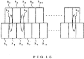
- Fig.15 is a schematic view illustrating the improvement for the resolution of the light-receiving element array.
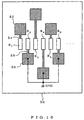
- Fig.16 is a plan view of one chip of a light-receiving element array of the third embodiment according to the present invention.
- Fig.17 is a cross-sectional view of a mesa-type light-receiving element array provided with electrodes.
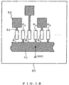
- Fig.18 is a plan view of another chip of a light-receiving element array of the third embodiment according to the present invention.
- Fig.19 is a plan view of another chip of a light-receiving element array of the third embodiment according to the present invention.
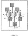
- Fig.20 is a plan view of another chip of a light-receiving element array of the third embodiment according to the present invention.
-
- The present embodiment is directed to a light demultiplexer in which a signal and a noise in the wavelength multiplexed light are distinctly separated, and a light-receiving element array used for a photodetector of the light demultiplexer.
- The structure of a light demultiplexer according to the present embodiment is substantially the same as that shown in Fig.1 except a photodetector. As the
photodetector 8, a light-emitting element array according to the present embodiment is used. An example of the light-receiving element array is shown in Fig.6. For monitoring N channels (N is an integer of 2 or more) of demultiplexed light beams, odd-numbered light-receiving elements for monitoring signals R1, R3, ···, R2N-1 and even-numbered light-receiving elements R2, R4, ···, R2N for monitoring noises are alternately arrayed. The total number of light-receiving elements is two times the number of demultiplexed light beams, i.e. 2N. According to this light-receiving element array, the element for monitoring a signal monitors the strength of a signal and the element for monitoring a noise monitors the strength of a noise. - For a first channel of demultiplexed light beam, the signal is monitored by the element R1, and the noise by the element R2. For a second channel of demultiplexed light beams, the signal is monitored by the element R3, and the noise by the elements R2, R4. For a last channel of demultiplexed light beam, the signal is monitored by the element R2N-1, and the noise by the elements R2N-2, R2N.
- For this light-receiving element array, the diffusion-type light-receiving element array as described with reference to Fig.2 may be used by way of example. As described above, Zn diffusion laterally proceeds in the element, so that the interval of elements may not be narrower than 50 µm, i.e. there is a limitation for the interval of elements.
- Fig.7 shows a plan view of a
chip 30 formed by the diffusion-type light-receiving element array. The elements for monitoring signals R1, R3, ···, R2N-1 and the elements for monitoring noises R2, R4, ···, R2N are connected tocorresponding bonding pads 36 through awiring 34, respectively. As described above, the interval p1 of elements is required to be larger than 50µm. - The mesa-type light-receiving as described in Fig.3 may also be used for a light-receiving element array. The mesa-type light-receiving element array may prevent the limitation of the interval of elements due to the lateral diffusion, which is the problem caused in the structure of the diffusion-type one as described above. As a result, a high-density light-receiving element array, such as 25µm or 10µm interval, may be provided.
- Fig.8 shows a plan view of a
chip 32 formed by the mesa-type light-receiving element array. As described above, the interval of elements may be small such as 10µ m. - Fig.9 shows a circuitry for detecting N channels of signal and noises which have been separated. This detecting circuitry comprises signal monitoring differential amplifiers D1, D3, ···, D2N-1 to one input terminal thereof the element for monitoring a signal is connected, noise monitoring differential amplifiers D2, D4, ···, D2N to one input terminal thereof the element for monitoring a noise is connected, and a signal/noise
monitoring output circuit 40. A reference level Iref is connected to the other input terminal of the signal monitoring differential amplifiers D1, D3, ···, D2N-1, and a reference level Nref is connected to the other input terminal of the noise monitoring differential amplifiers D2, D4, ···, D2N. The signals and noises are monitored based on those reference levels. - The operation of the light demultiplexer of the present invention will now be described with reference to Fig.1. The wavelength multiplexed light beam from the input
optical fiber 2 is converted into a parallel light beam by the collimator lens, and the parallel light beam reaches to thediffraction grating 6. The parallel light beam is separated every wavelength into a plurality of demultiplexed beams based on the wavelength dispersion characteristic of thediffraction grating 6. The demultiplexed light beams are converted into convergent light beams, respectively, by thecollimator lens 4. These convergent light beams impinge upon thephotodetector 16 which is positioned at a focal point of thecollimator lens 4. Fig.10 shows that all of the demultiplexed light beams impinge upon the light-receiving elements for monitoring the signals without causing the spread of spectral width and the shift of wavelength. In this case, each differential amplifier in Fig.9 does not output a signal, so that the signal/noisemonitoring output circuit 40 does not detect the spread of spectral width and the shift of wavelength. - On the contrary, Fig.11 shows that the peak wavelength of the demultiplexed light beam L1 is shifted from the normal value. As apparent from the shift condition of the demultiplexed light beam L1 shown in Fig.11, the detecting output of the light-receiving element R1 for monitoring a signal is decreased, and the detecting output of the light-receiving element R2 for monitoring a noise is increased.
- The differential amplifier D1 subtracts the reference level Iref from the signal output of the element R1 to output it as a signal. Also, the differential amplifier D2 subtracts the reference level Nref from the noise output of the element R2 to output it as a noise. The signal/noise
monitoring output circuit 40 may detect the shift of the peak position of the demultiplexed light beam L1, i.e. the shift of wavelength from the outputs of the differential amplifier D1, D2. - In the light-receiving element array shown in Fig.6, the odd-numbered elements are ones for monitoring signals and the even-numbered elements are ones for monitoring noises, but it is also possible that the even-numbered elements are ones for monitoring signals and the odd-numbered elements are ones for monitoring noises.
- Also, the array including 2N elements is illustrated for simplicity in Fig.6, but it may be possible to use only 2N elements in the array including more than 2N elements.
- Also, if (2N+1) elements are used to arrange the elements for monitoring noises at both ends of the light-receiving element array, then it is preferably performed to monitor noises at first and last channels. According to this, an additional element for monitoring a noise is necessarily arranged on the left side of the element R1 for monitoring a signal, so that a noise monitoring for the first channel of demultiplexed light beam L1 may be implemented by means of the additional element and element R2 for monitoring noises.
- In the case that noises between channels is desired to be monitored, the noises between channels may be monitored by (N-1) elements for monitoring noises, so that light-receiving element array may be structured by (2N-1) elements.
- The present embodiment is directed to a light demultiplexer in which the alignment between demultiplexed light beams and light-receiving elements may be precisely implemented as well as the resolution thereof may be improved, and a light-receiving element array used for a photodetector of the light demultiplexer.
- The structure of a light demultiplexer according to the present embodiment is substantially the same as that shown in Fig.1 except a photodetector. As the
photodetector 8, a light-emitting element array according to the present embodiment is used. The light-receiving element array will now be described with reference to Fig.12. In the figure, a light-receivingarray chip 48 constructed by two rows of element arrays is illustrated. One row of elements are designated by odd-numbered elements R1, R3, R5, R7, R9, ···, the other row of elements by even-numbered elements R2, R4, R6, R8, ···. The array pitch in one row of elements is the same as that of the other row of elements, and these two rows of elements are arrayed with one-half pitch shifted. - The elements R1, R3, R5, R7, R9, ··· in one row are connected to boding
pads 40 arranged opposing to the elements, through awiring 42, respectively, and the elements R2, R4, R6, R8, ··· in the other row are connected tobonding pads 44 arranged opposing to the elements through awiring 46, respectively. - The arrangement of boding pads is illustrated above by way of example, so it may be possible that all of the bonding pads are arrayed in one row on one side of the two rows of elements, i.e. near the side edge of the light-receiving element array chip.
- Next, the alignment between the two rows of light-receiving elements arrayed with one-half pitch shifted and the demultiplexed light beams will be described. Fig.13 shows the light-receiving element array consisting of two rows elements and the demultiplexed light beams (only the light beams L1, L2 and LN are designated in the figure). As apparent from the figure, each of the demultiplexed light beams impinges upon three light-receiving elements which are adjacent to each other in a direction perpendicular to an array direction of the two rows of elements. The output signals (current or voltage) from these three adjacent elements are monitored. In the light-receiving element array shown in Fig.13, the demultiplexed light beam L1 are monitored by the elements R2 R3, R4 and the light beam L2 by the element R6, R7, R8.
- According to the monitoring by means of three light-receiving elements which are adjacent to each other, the alignment of the demultiplexed light beams with respect to the light-receiving element array may be implemented at a high precision. For example, in order to align the center of the light beam L1 is aligned with respect to a contact point S of three adjacent elements R2, R3 and R4, respective amounts of light detected by the elements R2 and R4 are caused to be the same, and the sum of the amounts of light detected by the elements R2 and R4 is caused to be identical with the amount of light detected by the element R3. In Fig.13, the center point of the demultiplexed light beam L2 is designated to be shifted from the contact point S of the elements R6, R7, R8. According to this demultiplexed light beam L2, the respective amounts of light detected by the elements R6 and R8 are different, and the sum of amounts of light detected by the elements R6 and R8 is the same as the amount of light detected by the element R7, so that it is appreciated that the light beam L2 is shifted in an array direction of elements with respect to the contact point S.
- Furthermore, the resolution of the light-receiving element array may be improved, when the light-receiving' element array of the present embodiment is used. Figs.14 and 15 are the drawings for explanation of the improvement of the resolution. When two rows of light-receiving elements (the elements in each row are arrayed in 40 µm pitch, for example) are arrayed with one-half pitch shifted as shown in these figures, the overlap in an array direction between the element in one row and the element in the other row becomes 20µm.
- Therefore, the demultiplexed light beams L1, L2, ···, LN each light beam having a width of 10 µm in an array direction of elements are caused to impinge upon the light-receiving element array in the pitch equal to one-half of an array pitch of elements, in such a manner that the center point of each light beam is caused to be positioned substantially at the contact point S of three elements which are adjacent to each other. Consequently, it is appreciated that the resolution thereof may be two times compared to the conventional array consisting of one row of light-receiving elements.
- On the other hand, in the light-receiving element array in Fig.15 which is the same as that in Fig.14, when the demultiplexed light beam L1 having a width of 10 µm in an array direction of elements is positioned at the center portion of overlap area between the element R2 and R3, if the position of light beam L1 is shifted more than 5 µm in an array direction, then the element R1 or R4 which is adjacent to the element R2 and R3 may detect the light beam L1. Therefore, the resolution may be obtained, which is the same as that in the light-receiving element array consisting of one row of elements. That is, it is appreciated that the resolution may also be increased such as two times in the arrangement of the light beams in Fig.15.
- The present embodiment is directed to a light demultiplexer in which a crosstalk between adjacent light-receiving elements may be decreased, and a light-receiving element array used for a photodetector of the light demultiplexer.
- Fig.16 is a plan view of a light-receiving
element array chip 50. In the chip, a light-receiving element for monitoring a signal and a light-receiving element in which a p-type electrode and an n-type electrode thereof are shorted (hereinafter, referred to as an electrode shorted light-receiving element) are alternately arranged in turn from the left side. In the figure, the light-receiving element for monitoring a signal R1, the electrode shorted light-receiving element R2, the light-receiving element for monitoring a signal R3, the electrode shorted light-receiving element R4, the light-receiving element for monitoring a signal R5, and the electrode shorted light-receiving element R6 are shown in turn from the left side. - In the diffusion-type light-receiving element array shown in Fig.2, p-type electrodes (not shown) are provided on the p-
type regions 30, respectively, and a common n-type electrode (not shown) is provided on the bottom surface of the n-type InP substrate 22. The common n-type electrode is usually grounded. Therefore, the element in which the p-type electrode is grounded is the electrode shorted element. - In the mesa-type light-receiving element array in Fig.3, p-type electrodes (not shown) are provided on the p-type InP layers 27, respectively, and a common n-type electrode (not shown) is provided on the bottom surface of the n-
type InP substrate 22. Fig.17 shows the structure of a mesa-type light-receiving element provided with p-type electrodes 23 and an n-type electrode 25.Reference numeral 29 designates an insulting film. An n-type electrode may also be provided on the n-type InP layer 24 every light-receiving element. These n-type electrodes are usually grounded. Therefore, the light-receiving element in which the p-type electrode is grounded is an electrode shorted light-receiving element. - Returning to Fig.16, the p-type electrodes of the light-receiving elements for monitoring signals R1, R3, R5, ··· are connected to
bonding pads 52 through awiring 54, respectively. The common n-type electrode is connected to a bonding pad (not shown) which is grounded as described hereinafter.Bonding pads 56 of the electrode shorted light-receiving elements R2, R4, R6, ··· are commonly connected to the ground as described hereinafter. - In order to monitor N (N is an integer of 2 or more) demultiplexed light beams by light-receiving elements, about 2N light-receiving elements are required in this embodiment. The same effect may be obtained in all the cases that the number of light-receiving elements is 2N, (2N+1) or (2N-1). In the case of (2N+1), the elements on both sides of the light-receiving element array are the electrode shorted light-receiving elements. In the case of 2N, the element on one side of the array is the electrode shorted light-receiving element. In the case of (2N-1), the elements on both sides of the array are the light-receiving elements for monitoring signals.
- The light-receiving
element array chip 50 described above is in effect mounted in a package. Thebonding pads 52 of the light-receiving elements are connected to the leads of the package, respectively, the bonding pad (not shown) connected to the common n-type electrode is connected to one lead for grounding of the package, and thebonding pads 56 of the electrode shorted light-receiving elements are commonly connected to one or a few leads for grounding of the package. With respect to these leads, the signal detecting circuitry is connected, and such connection is implemented for forming the short circuit of electrodes on a printed circuit board. - A part of these connections may be in advance built in the light-receiving element array chip. An example of such light-receiving element array chip is shown in Fig.18. According to the light-receiving
element array chip 60 in the figure, ametal wiring pattern 70 is provided for commonly connecting the p-type electrodes of all the electrode shorted light-receiving elements in place of providing the bonding pads for the electrode shorted light-receiving elements. Themetal wiring pattern 70 is connected to one lead for grounding in the package. - In the light-receiving element array chips as shown in Figs.16 and 18, both the light-receiving element for monitoring a signal and the electrode shorted light-receiving element have the same form, so that the size of a chip becomes large. In order to make the size small, as shown in Fig.19, the width in an array direction of the electrode shorted elements R2, R4, R6, ··· is caused to be smaller than that of the elements for monitoring signals R1, R3, R5, ··· to make the array pitch of the light-receiving elements small. Also in this case, the
metal wiring pattern 70 shown in Fig.18 may be used in place of providing the bodingpads 56 for the electrode shorted light-receiving elements. - In the case that the light-receiving element array illustrated in Figs.16, 18 and 19 is the diffusion-type light-receiving element array, the carrier diffused from the element for monitoring a signal is captured by the electrode shorted element, so that the carrier may not reach to the adjacent element for monitoring a signal. Therefore, a crosstalk may be largely decreased.
- In the case that the light-receiving element array is the mesa-type light-receiving element array, if light. impinges upon the electrode shorted light-receiving element, a crosstalk is not caused because there is the electrode shorted light-receiving element between the light-receiving elements for monitoring signals.
- In the embodiments illustrated in Figs.16, 18 and 19, if light impinges upon the electrode shorted light-receiving element, then the carrier is generated. It is undesirable that the carrier is diffused into the light-receiving element for monitoring a signal to cause an undesirable current. The undesirable current is a factor of varying locally the temperature of the light-receiving element. Therefore, it is desirable that the light-receiving surface of the electrode shorted element is shielded for light in advance. The light shielding is carried out as shown in Fig.20 by covering the light-receiving surfaces of the electrode shorted light-receiving elements R2, R4, R6, ··· with the light shielding layers 82, 84, 86, ···. The electrode shorted light-receiving elements may also be connected together by the
metal wiring pattern 70 as shown in Fig.18, and may also have a smaller light-receiving surface as shown in Fig.19. - When the light-receiving element array according to the present invention is used, the light demultiplexers may be provided, such as (1) the light demultiplexer in which a signal and a noise in each channel may be distinctly separated, (2) the light demultiplexer in which the alignment between demultiplexed light beams and light-receiving elements may be precisely implemented as well as the resolution of a light demultiplexer may be improved, and (3) the light demultiplexer in which a crosstalk between adjacent light-receiving elements may be decreased.
Claims (16)
- A light-receiving element array for receiving light beams demultiplexed every wavelength from a wavelength multiplexed light beam and arranged in a straight line, comprising :a plurality of light-receiving elements for monitoring signals, anda plurality of light-receiving elements for monitoring noises,wherein the light-receiving elements for monitoring signals and the light-receiving elements for monitoring noise are alternately arrayed in a straight line the direction thereof is the same as that of the arrangement of the demultiplexed light beams.
- The light-receiving element array according to claim 1, wherein the light-receiving elements for monitoring signals and the light-receiving elements for monitoring noise are consisting of pin-photodiodes, respectively.
- A light demultiplexer, comprising:a light-receiving element array according to claim 1 or 2 for receiving light beams demultiplexed every wavelength from a wavelength multiplexed light beam and arranged in a straight line,wherein the signals and noises are separated to be monitored by the light-receiving element array.
- A light-receiving element array for receiving light beams demultiplexed every wavelength from a wavelength multiplexed light beam and arranged in a straight line, comprising :a first row of light-receiving elements arrayed in a predetermined pitch and in the same direction as that of the arrangement of the demultiplexed light beams, anda second row of light-receiving elements arrayed in the same pitch as the predetermined pitch and in the same direction as that of the arrangement of the demultiplexed light beams,wherein the first and second rows of light-receiving elements are arrayed with one-half pitch shifted in an array direction.
- The light-receiving element array according to claim 4, wherein the light-receiving elements are consisting of pin-photodiodes, respectively.
- A light demultiplexer, comprising:a light-receiving element array according to claim 4 or 5 for receiving light beams demultiplexed every wavelength from a wavelength multiplexed light beam and arranged in a straight line,wherein the demultiplexed light beams are monitored by the light-receiving element array.
- A method for aligning light-receiving element and demodulated light beams in a light demultiplexer including a light-receiving element array according to claim 4 or 5 for receiving light beams demultiplexed every wavelength from a wavelength multiplexed light beam and arranged in a straight line, the demultiplexed light beams being monitored by the light-receiving element array, said method comprising :a step of aligning the light-receiving element and the demodulated light beams by using output signals from three light-receiving elements which are adjacent to each other in a direction perpendicular to the array direction of the first and second rows of light-receiving elements.
- A light-receiving element array for receiving light beams demultiplexed every wavelength from a wavelength multiplexed light beam and arranged in a straight line, comprising :a plurality of light-receiving elements for monitoring signals, anda plurality of electrode shorted light-receiving elements,wherein the light-receiving elements for monitoring signals and the electrode shorted light-receiving elements are alternately arrayed in a straight line the direction thereof is the same as that of the arrangement of the demultiplexed light beams.
- The light-receiving element array according to claim 8, wherein the light-receiving elements for monitoring signals and the electrode shorted light-receiving elements are consisting of pin-photodiodes, respectively.
- The light-receiving element array according to claim 9, wherein the pin-photodiode comprising :an n-type semiconductor layer, an i-type semiconductor layer and a n-type semiconductor layer stacked in this order on a n-type semiconductor substrate,a p-type region which is formed by diffusing partially p-type material into the n-type semiconductor layer which is an uppermost layer,a p-type electrode provided on the p-type region, anda common n-type electrode provided on a bottom surface of the n-type semiconductor substrate.
- The light-receiving element array according to claim 9, wherein the pin-photodiode comprises :an n-type semiconductor layer, an i-type semiconductor layer and a p-type semiconductor layer stacked in this order on a n-type semiconductor substrate, the p-type and i-type semiconductor layers are isolated by an isolating trench from the adjacent p-type and i-type semiconductor layers,a p-type electrode provided on the p-type semiconductor layer, anda common n-type electrode provide on a bottom surface of the n-type semiconductor substrate.
- The light-receiving element array according to claim 10 or 11, wherein the p-type electrode of the electrode shorted light-receiving element is shorted to the common n-type electrode.
- The light-receiving element array according to claim 10 or 11, wherein the p-type electrode of the electrode shorted light-receiving element is connected to one common metallic wiring which is shorted to the common n-type electrode.
- The light-receiving element array according to claim 8 or 9, wherein the element area of the electrode shorted light-receiving element is smaller than that of the light-receiving element for monitoring a signal.
- The light-receiving element array according to claim 8 or 9, wherein the light-receiving surface of the electrode shorted light-receiving element is provided with a light shielding film.
- A light demultiplexer, comprising:a light-receiving element array according to claim 8 or 9 for receiving light beams demultiplexed every wavelength from a wavelength multiplexed light beam and arranged in a straight line, andwherein the demultiplexed light beams are monitored by the light-receiving element array.
Applications Claiming Priority (7)
| Application Number | Priority Date | Filing Date | Title |
|---|---|---|---|
| JP28776499 | 1999-10-08 | ||
| JP28776499A JP3683445B2 (en) | 1999-10-08 | 1999-10-08 | Optical demultiplexer |
| JP32200499A JP2001141566A (en) | 1999-11-12 | 1999-11-12 | Optical demultiplexer and photodetector array |
| JP32200499 | 1999-11-12 | ||
| JP2000001928 | 2000-01-07 | ||
| JP2000001928 | 2000-01-07 | ||
| PCT/JP2000/006938 WO2001027573A1 (en) | 1999-10-08 | 2000-10-05 | Photodetector array and optical branching filter using the array |
Publications (1)
| Publication Number | Publication Date |
|---|---|
| EP1156311A1 true EP1156311A1 (en) | 2001-11-21 |
Family
ID=27337380
Family Applications (1)
| Application Number | Title | Priority Date | Filing Date |
|---|---|---|---|
| EP00964677A Withdrawn EP1156311A1 (en) | 1999-10-08 | 2000-10-05 | Photodetector array and optical branching filter using the array |
Country Status (6)
| Country | Link |
|---|---|
| US (1) | US7062178B1 (en) |
| EP (1) | EP1156311A1 (en) |
| CN (1) | CN1327532A (en) |
| CA (1) | CA2354267A1 (en) |
| TW (1) | TW477076B (en) |
| WO (1) | WO2001027573A1 (en) |
Cited By (3)
| Publication number | Priority date | Publication date | Assignee | Title |
|---|---|---|---|---|
| US7113282B2 (en) | 2003-12-19 | 2006-09-26 | 3M Innonative Properties Company | Multiplexing rotary spectrometer |
| EP1731887A1 (en) * | 2005-06-09 | 2006-12-13 | Yokogawa Electric Corporation | Photodiode array |
| EP1178535A3 (en) * | 2000-08-02 | 2008-07-16 | Nippon Sheet Glass Co., Ltd. | Photodetector array and optical communication monitoring |
Families Citing this family (3)
| Publication number | Priority date | Publication date | Assignee | Title |
|---|---|---|---|---|
| CN101694453B (en) * | 2009-09-29 | 2011-07-20 | 深圳市蓝韵实业有限公司 | Anti-crosstalk biochemistry analyzer detector device |
| JP5971843B2 (en) | 2011-05-18 | 2016-08-17 | 日本オクラロ株式会社 | Array type light receiving device, optical receiving module, and optical transceiver |
| JP2012244061A (en) * | 2011-05-23 | 2012-12-10 | Mitsubishi Electric Corp | Semiconductor photodetector |
Family Cites Families (10)
| Publication number | Priority date | Publication date | Assignee | Title |
|---|---|---|---|---|
| GB862212A (en) * | 1956-06-08 | 1961-03-08 | Renault | Improvements in or relating to apparatus for the direct analysis of spectral lines |
| US3535537A (en) * | 1968-04-09 | 1970-10-20 | Us Navy | Optical line splitter having light conducting strips with fused input end and flared output ends |
| US4146332A (en) | 1977-04-19 | 1979-03-27 | The United States Of America As Represented By The Secretary Of The Navy | Spectrometer with electronic readout |
| JP3067880B2 (en) * | 1991-01-12 | 2000-07-24 | キヤノン株式会社 | Photodetector having diffraction grating |
| JP3230565B2 (en) * | 1996-02-07 | 2001-11-19 | 横河電機株式会社 | Optical spectrum analyzer |
| JP3720112B2 (en) * | 1996-03-18 | 2005-11-24 | 富士通株式会社 | System and optical power control apparatus to which wavelength division multiplexing is applied |
| KR100312224B1 (en) * | 1998-07-02 | 2001-12-20 | 윤종용 | Optical signal-to-noise ratio measuring device in wavelength division multiplexing optical transmitter |
| US6580536B1 (en) * | 1999-01-14 | 2003-06-17 | Lucent Technologies Inc. | Power and wavelength management for mixed-rate optical data systems |
| JP3642209B2 (en) * | 1999-01-22 | 2005-04-27 | 横河電機株式会社 | Optical spectrum monitor |
| US6420985B1 (en) * | 1999-04-20 | 2002-07-16 | Ensco Inc. | Photonic wide-band analog to digital converter and method |
-
2000
- 2000-10-05 CN CN00802203A patent/CN1327532A/en active Pending
- 2000-10-05 US US09/857,634 patent/US7062178B1/en not_active Expired - Fee Related
- 2000-10-05 WO PCT/JP2000/006938 patent/WO2001027573A1/en not_active Ceased
- 2000-10-05 CA CA002354267A patent/CA2354267A1/en not_active Abandoned
- 2000-10-05 EP EP00964677A patent/EP1156311A1/en not_active Withdrawn
- 2000-10-06 TW TW089120867A patent/TW477076B/en not_active IP Right Cessation
Non-Patent Citations (1)
| Title |
|---|
| See references of WO0127573A1 * |
Cited By (3)
| Publication number | Priority date | Publication date | Assignee | Title |
|---|---|---|---|---|
| EP1178535A3 (en) * | 2000-08-02 | 2008-07-16 | Nippon Sheet Glass Co., Ltd. | Photodetector array and optical communication monitoring |
| US7113282B2 (en) | 2003-12-19 | 2006-09-26 | 3M Innonative Properties Company | Multiplexing rotary spectrometer |
| EP1731887A1 (en) * | 2005-06-09 | 2006-12-13 | Yokogawa Electric Corporation | Photodiode array |
Also Published As
| Publication number | Publication date |
|---|---|
| CA2354267A1 (en) | 2001-04-19 |
| WO2001027573A1 (en) | 2001-04-19 |
| TW477076B (en) | 2002-02-21 |
| CN1327532A (en) | 2001-12-19 |
| US7062178B1 (en) | 2006-06-13 |
Similar Documents
| Publication | Publication Date | Title |
|---|---|---|
| US6690002B2 (en) | Photodetector array and optical communication monitor module using the same | |
| US6373606B1 (en) | Optical demultiplexer | |
| US7332751B2 (en) | Rear-illuminated-type photodiode array | |
| US5206920A (en) | Integrated optical arrangement for demultiplexing a plurality of different wavelength channels and the method of manufacture | |
| KR101075626B1 (en) | Photodetector | |
| EP1182705A1 (en) | Light-receiving element array and light-receiving element array chip | |
| US6828541B2 (en) | Light receiving element array having isolated pin photodiodes | |
| US6949770B2 (en) | Photodiode array and optical receiver device including the same | |
| US7062178B1 (en) | Photodetector array and optical branching filter using the array | |
| US20120292731A1 (en) | Light-receiving device allay, optical receiver module, and optical transceiver | |
| CN101075849B (en) | Multi-channel Optical Receiver Module | |
| EP1133082A1 (en) | Optical monitoring system | |
| US7372124B2 (en) | Light-receiving element and photodetector using the same | |
| JP2004303878A (en) | Photodetector array | |
| JP3683445B2 (en) | Optical demultiplexer | |
| US6424760B1 (en) | Optical multiplexer/demultiplexer | |
| WO2004017428A1 (en) | Wavelength-demultiplexer with integrated monolithic photodiodes | |
| JP2020141065A (en) | Manufacturing method of photoelectric conversion element, optical subassembly and photoelectric conversion element | |
| JP2700262B2 (en) | Light detection method | |
| KR20200137959A (en) | Multi-color photo detector and method for fabricating the same by integrating with read-out circuit | |
| JPS63164279A (en) | Photodetector | |
| WO2002086570A1 (en) | Optical demultiplexer |
Legal Events
| Date | Code | Title | Description |
|---|---|---|---|
| PUAI | Public reference made under article 153(3) epc to a published international application that has entered the european phase |
Free format text: ORIGINAL CODE: 0009012 |
|
| AK | Designated contracting states |
Kind code of ref document: A1 Designated state(s): AT BE CH CY DE DK ES FI FR GB GR IE IT LI LU MC NL PT SE |
|
| AX | Request for extension of the european patent |
Free format text: AL;LT;LV;MK;RO;SI |
|
| 17P | Request for examination filed |
Effective date: 20010921 |
|
| STAA | Information on the status of an ep patent application or granted ep patent |
Free format text: STATUS: THE APPLICATION HAS BEEN WITHDRAWN |
|
| 18W | Application withdrawn |
Effective date: 20030922 |