EP1155778B1 - Polishing apparatus - Google Patents
Polishing apparatus Download PDFInfo
- Publication number
- EP1155778B1 EP1155778B1 EP01111685A EP01111685A EP1155778B1 EP 1155778 B1 EP1155778 B1 EP 1155778B1 EP 01111685 A EP01111685 A EP 01111685A EP 01111685 A EP01111685 A EP 01111685A EP 1155778 B1 EP1155778 B1 EP 1155778B1
- Authority
- EP
- European Patent Office
- Prior art keywords
- polishing
- wafer
- semiconductor wafer
- top ring
- cleaning
- Prior art date
- Legal status (The legal status is an assumption and is not a legal conclusion. Google has not performed a legal analysis and makes no representation as to the accuracy of the status listed.)
- Expired - Lifetime
Links
Images























Classifications
-
- H—ELECTRICITY
- H10—SEMICONDUCTOR DEVICES; ELECTRIC SOLID-STATE DEVICES NOT OTHERWISE PROVIDED FOR
- H10P—GENERIC PROCESSES OR APPARATUS FOR THE MANUFACTURE OR TREATMENT OF DEVICES COVERED BY CLASS H10
- H10P72/00—Handling or holding of wafers, substrates or devices during manufacture or treatment thereof
- H10P72/04—Apparatus for manufacture or treatment
- H10P72/0451—Apparatus for manufacturing or treating in a plurality of work-stations
- H10P72/0468—Apparatus for manufacturing or treating in a plurality of work-stations comprising a chamber adapted to a particular process
- H10P72/0472—Apparatus for manufacturing or treating in a plurality of work-stations comprising a chamber adapted to a particular process comprising at least one polishing chamber
-
- B—PERFORMING OPERATIONS; TRANSPORTING
- B24—GRINDING; POLISHING
- B24B—MACHINES, DEVICES, OR PROCESSES FOR GRINDING OR POLISHING; DRESSING OR CONDITIONING OF ABRADING SURFACES; FEEDING OF GRINDING, POLISHING, OR LAPPING AGENTS
- B24B37/00—Lapping machines or devices; Accessories
- B24B37/34—Accessories
- B24B37/345—Feeding, loading or unloading work specially adapted to lapping
-
- B—PERFORMING OPERATIONS; TRANSPORTING
- B24—GRINDING; POLISHING
- B24B—MACHINES, DEVICES, OR PROCESSES FOR GRINDING OR POLISHING; DRESSING OR CONDITIONING OF ABRADING SURFACES; FEEDING OF GRINDING, POLISHING, OR LAPPING AGENTS
- B24B41/00—Component parts such as frames, beds, carriages, headstocks
- B24B41/06—Work supports, e.g. adjustable steadies
- B24B41/061—Work supports, e.g. adjustable steadies axially supporting turning workpieces, e.g. magnetically, pneumatically
-
- H—ELECTRICITY
- H10—SEMICONDUCTOR DEVICES; ELECTRIC SOLID-STATE DEVICES NOT OTHERWISE PROVIDED FOR
- H10P—GENERIC PROCESSES OR APPARATUS FOR THE MANUFACTURE OR TREATMENT OF DEVICES COVERED BY CLASS H10
- H10P72/00—Handling or holding of wafers, substrates or devices during manufacture or treatment thereof
- H10P72/30—Handling or holding of wafers, substrates or devices during manufacture or treatment thereof for conveying, e.g. between different workstations
- H10P72/33—Handling or holding of wafers, substrates or devices during manufacture or treatment thereof for conveying, e.g. between different workstations into and out of processing chamber
- H10P72/3304—Handling or holding of wafers, substrates or devices during manufacture or treatment thereof for conveying, e.g. between different workstations into and out of processing chamber characterised by movements or sequence of movements of transfer devices
-
- H—ELECTRICITY
- H10—SEMICONDUCTOR DEVICES; ELECTRIC SOLID-STATE DEVICES NOT OTHERWISE PROVIDED FOR
- H10P—GENERIC PROCESSES OR APPARATUS FOR THE MANUFACTURE OR TREATMENT OF DEVICES COVERED BY CLASS H10
- H10P72/00—Handling or holding of wafers, substrates or devices during manufacture or treatment thereof
- H10P72/70—Handling or holding of wafers, substrates or devices during manufacture or treatment thereof for supporting or gripping
- H10P72/76—Handling or holding of wafers, substrates or devices during manufacture or treatment thereof for supporting or gripping using mechanical means, e.g. clamps or pinches
- H10P72/7604—Handling or holding of wafers, substrates or devices during manufacture or treatment thereof for supporting or gripping using mechanical means, e.g. clamps or pinches the wafers being placed on a susceptor, stage or support
- H10P72/7626—Handling or holding of wafers, substrates or devices during manufacture or treatment thereof for supporting or gripping using mechanical means, e.g. clamps or pinches the wafers being placed on a susceptor, stage or support characterised by the construction of the shaft
Definitions
- the present invention relates to a polishing apparatus for polishing a workpiece such as a semiconductor wafer to a flat mirror finish, and more particularly to a multi-head type polishing apparatus having a plurality of top rings for holding workpieces with respect to a single polishing table.
- One customary way of planarizing the surface of the semiconductor wafer is to polish the semiconductor wafer by a chemical mechanical polishing (CMP) process.
- CMP chemical mechanical polishing
- a multi-head type polishing apparatus which has a plurality of top rings for holding semiconductor wafers with respect to a single polishing table and can polish a plurality of semiconductor wafers simultaneously.
- semiconductor wafers are mounted on the respective top rings, and then all of the semiconductor wafers held by the top rings are simultaneously pressed against a polishing surface of the polishing table and polished. After polishing of the semiconductor wafers is conducted for a predetermined time, all of the top rings holding the semiconductor wafers are raised from the polishing table, and then all of the semiconductor wafers which have been polished are removed from the top rings. Thereafter, new semiconductor wafers are mounted on the top rings.
- the conventional multi-head type polishing apparatus is a dedicated polishing apparatus for conducting only polishing of semiconductor wafers, and hence the semiconductor wafers which have been polished are transported to a next cleaning process by a movable container in which they are immersed in water to keep them from drying during transportation.
- a movable container in which they are immersed in water to keep them from drying during transportation.
- the cleanliness of a clean room tends to be impaired, and the polished semiconductor wafers need to be transported by an operator or a manually operated transportation means.
- a large installation space is required for two kinds of apparatuses comprising the polishing apparatus and the cleaning apparatus that is used to carry out the subsequent cleaning process.
- a multi-head type polishing apparatus which performs both a polishing process and a cleaning process therein and is of a dry-in and dry-out type for introducing semiconductor wafers therein in a dry condition and removing polished and cleaned semiconductor wafers therefrom in a dry condition.
- U.S. Patent 5,329,732 shows a polishing apparatus having a multi-head comprising a polishing table, a plurality of top rings (carriers) attached to a polishing assembly, a rotary transporter (index table) and a plurality of pushers for transferring workpieces between said index table and said carriers.
- the polishing assembly as a whole is moved along a linear rail from a position above the polishing table to a position above the index table. After transfer of the substrates the polishing assembly is again moved as a whole back to a position above the polishing table.
- each wafer carrier is oscillated by a polish arm attached to the polishing assembly.
- a polishing apparatus having a multi-head, comprising: a polishing table having a polishing surface; a plurality of top rings for holding workpieces and pressing the workpieces against the polishing surface; a carousel for supporting the top rings and indexing the top rings; a rotary transporter disposed in a position which can be accessed by the top rings and having a plurality of portions positioned on a predetermined circumference from a center of rotation of the rotary transporter for holding the workpieces, the rotary transporter having an indexing function for indexing the plurality of portions; and a pusher for transferring the workpieces between the rotary transporter and the top rings, wherein each of said top rings is connected to said carousel through a swing arm, and is angularly movable by said swing arm to a polishing position on said polishing table and a loading and unloading position on said rotary transporter.
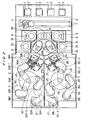
- FIG. 1 shows a layout of various components of a polishing apparatus.
- a polishing apparatus comprises four load-unload stages 2 each for placing a wafer cassette 1 which accommodates a plurality of semiconductor wafers.
- the load-unload stage 2 may have a mechanism for raising and lowering the wafer cassette 1.
- a transfer robot 4 having two hands is provided on rails 3 so that the transfer robot 4 can move along the rails 3 and access the respective wafer cassettes 1 on the respective load-unload stages 2.
- the transfer robot 4 has two hands which are located in a vertically spaced relationship, and the lower hand is used only for taking out a semiconductor wafer from the wafer cassette 1 and the upper hand is used only for returning the semiconductor wafer to the wafer cassette 1.
- This arrangement allows that a clean semiconductor wafer which has been cleaned is placed at an upper side and is not contaminated.
- the lower hand is a vacuum attraction-type hand for holding a semiconductor wafer under vacuum
- the upper hand is a recess support-type hand for supporting a peripheral edge of a semiconductor wafer by a recess formed on the hand.
- the vacuum attraction-type hand can hold a semiconductor wafer and transport the semiconductor wafer even if the semiconductor wafer is not located at a normal position in the wafer cassette due to a slight displacement, and the recess support-type hand can transport a semiconductor wafer while keeping the semiconductor wafer clean because dust is not collected unlike the vacuum attraction-type hand.
- Two cleaning apparatuses 5 and 6 are disposed at the opposite side of the wafer cassettes 1 with respect to the rails 3 of the transfer robot 4.
- the cleaning apparatuses 5 and 6 are disposed at positions that can be accessed by the hands of the transfer robot 4.
- a wafer station 90 having multi-stage wafer supports (wafer trays) in a vertical direction.
- the cleaning apparatuses 5 and 6 have a spin-dry mechanism for drying a semiconductor wafer by spinning the semiconductor wafer at a high speed, and hence the two-stage cleaning or three-stage cleaning of the semiconductor wafer can be conducted without replacing any cleaning module.
- An area B in which the cleaning apparatuses 5 and 6 and the wafer station 90 are disposed and an area A in which the wafer cassettes 1 and the transfer robot 4 are disposed are partitioned by a partition wall 14 so that the cleanliness of the area B and the area A can be separated.
- the partition wall 14 has an opening for allowing semiconductor wafers to pass therethrough, and a shutter 11 is provided at the opening of the partition wall 14.
- a transfer robot 20 having two hands is disposed at a position where the transfer robot 20 can access the cleaning apparatus 5 and the wafer station 90, and a transfer robot 21 having two hands is disposed at a position where the transfer robot 21 can access the cleaning apparatus 6 and the wafer station 90.
- the transfer robot 20 and the transfer robot 21 have the respective two hands which are located in a vertically spaced relationship.
- the respective upper hands of the transfer robot 20 and the transfer robot 21 are used for transporting a semiconductor wafer which has been cleaned to the cleaning apparatuses or wafer trays of the wafer station 90, and the respective lower hands of the transfer robot 20 and the transfer robot 21 are used for transporting a semiconductor wafer which has not cleaned or a semiconductor wafer to be polished. Since the lower hand is used to transfer a semiconductor wafer to or from a reversing device, the upper hand is not contaminated by drops of a rinsing water which fall from an upper wall of the reversing device.
- a cleaning apparatus 22 is disposed at a position adjacent to the cleaning apparatus 5 and accessible by the hands of the transfer robot 20, and another cleaning apparatus 23 is disposed at a position adjacent to the cleaning apparatus 6 and accessible by the hands of the transfer robot 21.
- All the cleaning apparatuses 5, 6, 22 and 23, the wafer station 90, and the transfer robots 20 and 21 are placed in the area B.
- the pressure in the area B is adjusted so as to be lower than the pressure in the area A.
- Each of the cleaning apparatuses 22 and 23 is capable of cleaning both surfaces of a semiconductor wafer.
- the polishing apparatus has a housing 100 for enclosing various components therein.
- the interior of the housing 100 is partitioned into a plurality of compartments or chambers (including the areas A and B) by partitions 14, 15, 16, 24 and 25.
- a polishing chamber separated from the area B by the partition wall 24 is formed, and is further divided into two areas C and D by the partition wall 25.
- An abrasive liquid nozzle (not shown) for supplying an abrasive liquid to the polishing table 34L and a dresser 38L for dressing the polishing table 34L are disposed in the area C.
- An abrasive liquid nozzle (not shown) for supplying an abrasive liquid to the polishing table 34R and a dresser 38R for dressing the polishing table 34R are disposed in the area D.
- a dresser 39L for dressing the polishing table 35L is disposed in the area C, and a dresser 39R for dressing the polishing table 35R is disposed in the area D.
- the polishing units disposed on the left and right sides are disposed in line symmetry with respect to the partition wall 25.
- the both polishing units have the respective three top rings 32L and 32R which hold the semiconductor wafers and polish them.
- a reversing device 28L for reversing a semiconductor wafer
- a reversing device 28R for reversing a semiconductor wafer.
- the partition wall 24 between the area B and the areas C, D has two openings each for allowing semiconductor wafers to pass therethrough, one of which is used for transferring the semiconductor wafer to or from the reversing device 28L and the other of which is used for transferring the semiconductor wafer to or from the reversing device 28R.
- Shutters 26L and 26R are provided at the respective openings of the partition wall 24.
- the reversing devices 28L and 28R have a chuck mechanism for chucking a semiconductor wafer, a reversing mechanism for reversing a semiconductor wafer, and a semiconductor wafer detecting sensor for detecting whether the chuck mechanism chucks a semiconductor wafer or not, respectively.
- the transfer robot 20 transfers a semiconductor wafer to the reversing device 28L, and the transfer robot 21 transfers a semiconductor wafer to the reversing device 28R.
- a rotary transporter 27L is disposed in the area C for transferring semiconductor wafers between the reversing device 28L and the three top ring 32L supported by the carousel 36L.
- the rotary transporter 27L has four stages for placing a semiconductor wafer at angularly equal intervals, and can hold a plurality of semiconductor wafers thereon at the same time.
- the semiconductor wafer which has been transported to the reversing device 28L is transferred to the rotary transporter 27L by actuating a lifter 29L disposed below the rotary transporter 27L when the center of the stage of the rotary transporter 27L is aligned with the center of the semiconductor wafer held by the reversing device 28L.
- the semiconductor wafer placed on the stage of the rotary transporter 27L is transported to a position above a pusher 30L by the indexing motion of the rotary transporter 27L.
- the top ring 32L is located at a position above the rotary transporter 27L (loading and unloading position) beforehand by a swing motion thereof.
- the semiconductor wafer is transferred from the rotary transporter 27L to the top ring 32L by actuating the pusher 30L disposed below the rotary transporter 27L when the center of the top ring 32L is aligned with the center of the semiconductor wafer placed on the stage of the rotary transporter 27L.
- the semiconductor wafers are sequentially loaded on the three top rings 32L supported by the carousel 36L.
- the semiconductor wafer transferred to the top ring 32L is held under vacuum by a vacuum attraction mechanism of the top ring 32L, and transported to the polishing table 34L. Thereafter, the semiconductor wafer is polished by a polishing surface comprising a polishing cloth or a grinding stone (or a fixed abrasive plate) attached on the polishing table 34L.
- the second polishing tables 35L is disposed at a position that can be accessed by the top rings 32L when the top ring 32L is located at an accessible position to the second polishing table 35L. With this arrangement, a primary polishing of the semiconductor wafer can be conducted by the polishing table 34L, and then a secondary polishing of the semiconductor wafer can be conducted by the second polishing table 35L. In this case, a buffing polishing of the semiconductor wafer can be conducted by the second polishing table 35L.
- a rotary transporter 27R is disposed in the area D for transferring semiconductor wafers between the reversing device 28R and the three top ring 32R supported by the carousel 36R.
- the rotary transporter 27R has four stages for placing a semiconductor wafer at angularly equal intervals, and can hold a plurality of semiconductor wafers thereon at the same time.
- the semiconductor wafer which has been transported to the reversing device 28R is transferred to the rotary transporter 27R by actuating a lifter 29R disposed below the rotary transporter 27R when the center of the stage of the rotary transporter 27R is aligned with the center of the semiconductor wafer held by the reversing device 28R.
- the semiconductor wafer placed on the stage of the rotary transporter 27R is transported to a position above a pusher 30R by the indexing motion of the rotary transporter 27R.
- the top ring 32R is located at a position above the rotary transporter 27R (loading and unloading position) beforehand by a swing motion thereof.
- the semiconductor wafer is transferred from the rotary transporter 27R to the top ring 32R by actuating the pusher 30R disposed below the rotary transporter 27R when the center of the top ring 32R is aligned with the center of the semiconductor wafer placed on the stage of the rotary transporter 27R.
- the semiconductor wafers are sequentially loaded on the three top rings 32R supported by the carousel 36R.
- the semiconductor wafer transferred to the top ring 32R is held under vacuum by a vacuum attraction mechanism of the top ring 32R, and transported to the polishing table 34R. Thereafter, the semiconductor wafer is polished by a polishing surface comprising a polishing cloth or a grinding stone (or a fixed abrasive plate) attached on the polishing table 34R.
- the second polishing tables 35R is disposed at a position that can be accessed by the top rings 32R when the top ring 32R is located at an accessible position to the second polishing table 35R. With this arrangement, a primary polishing of the semiconductor wafer can be conducted by the polishing table 34R, and then a secondary polishing of the semiconductor wafer can be conducted by the second polishing table 35R. In this case, a buffing polishing of the semiconductor wafer can be conducted by the second polishing table 35R.
- a cleaning liquid is supplied from cleaning liquid nozzles (not shown) disposed adjacent to the polishing table 34L or 34R to the lower and side surfaces of the semiconductor wafer held by the top ring 32L or 32R at a position where the top ring 32L or 32R is spaced from the polishing table 34L or 34R. Because the semiconductor wafer is rinsed before moving to the second polishing table 35L or 35R, the transfer of contamination between the polishing tables is prevented to thus avoid cross contamination of the polishing tables.
- the dressing process is a process for recovering the polishing surface of the polishing table which has been degraded by polishing of the semiconductor wafers. This process is also called conditioning or rectification.
- the semiconductor wafer which has been polished is transferred from the top ring 32L to the pusher 30L, and then transferred from the pusher 30L to the rotary transporter 27L by lowering the pusher 30L. Thereafter, the semiconductor wafer is transported to a position below the reversing device 28L by the indexing motion of the rotary transporter 27L, and then returned to the reversing device 28L by raising the lifter 29L.
- the semiconductor wafer which has been polished is transferred from the top ring 32R to the pusher 30R, and then transferred from the pusher 30R to the rotary transporter 27R by lowering the pusher 30R. Thereafter, the semiconductor wafer is transported to a position below the reversing device 28R by the indexing motion of the rotary transporter 27R, and then returned to the reversing device 28R by raising the lifter 29R.
- the semiconductor wafer returned to the reversing device 28L or 28R by the above operation is rinsed by pure water or chemicals supplied from rinsing nozzles. Further, the semiconductor wafer holding surface of the top ring 32L or 32R from which the semiconductor wafer has been removed is also cleaned by pure water or chemicals supplied from top ring cleaning nozzles, and in some cases, the semiconductor wafer holding surface of the top ring 32L or 32R is rinsed for preventing the semiconductor wafer holding surface from being dried.
- Pusher cleaning nozzles are provided on the partition wall to clean each of the pushers.
- the semiconductor wafer may be rinsed with chemicals in such a state that the semiconductor wafer is held by the top ring under vacuum. Furthermore, the semiconductor wafer may be rinsed with chemicals in such a state that the semiconductor wafer is held by the rotary transporter 27L or 27R above the pusher. The lifter may be cleaned by nozzles described below.
- FIG. 2 shows the polishing units on the left and right sides in which the three top rings 32L, 32R perform different operations.
- the top ring 32L-1 is located in the loading and unloading position
- the top ring 32L-2 is located in the overhanging position with respect to the polishing table 34L
- the top ring 32L-3 is located on the second polishing table 35L.
- the top ring 32R-1 accesses the loading and unloading position
- the top ring 32R-2 accesses the polishing table 35R
- the top ring 32R-3 is located away from the polishing table 34R.
- Other components or devices are in the same condition as those in FIG. 1.
- the dressers 38L and 38 R are supported by respective dresser heads 60.
- the dresser heads 60 are supported by respective swing shafts which are capable of positionally being fixed, and the dressers 38L and 38R are movable between respective standby positions and respective dressing positions on the respective polishing tables 34L and 34R.
- the dressers 39L and 39R are supported by respective dresser heads 61.
- the dresser heads 61 are supported by respective swing shafts which are capable of being positionally fixed, and the dressers 39L and 39R are movable between respective standby positions and respective dressing positions on the respective polishing tables 35L and 35R.
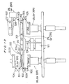
- FIGS. 3 through 5 show the relationship between multi-head type top rings 32L (or 32R) supported by the carousel 36L (or 36R) and the polishing table 34L (or 34R).
- FIG. 3 is a schematic side view and FIGS. 4 and 5 are schematic perspective views.
- the carousels 36L and 36R, the top rings 32L and 32R, and the polishing table 34L and 34R on the left and right sides have the same structure, and hence only the carousel 36L, the top rings 32L and the polishing table 34L on the left side will be described.
- the carousel 36L is supported by a support member 42 which is supported by a plurality of posts 41 (in FIG. 3, only one post is shown).
- the carousel 36L is supported from the support member 42 by a main shaft 43 which is rotatable.
- the main shaft 43 is coupled to a motor 44 fixed to the support member 42. Therefore, the carousel 36L is rotatable about a vertical axis O by rotating the main shaft 43.
- the carousel 36L supports three top ring swing arms 45 (in FIG. 3, only one swing arm is shown).
- Each of the top ring swing arms 45 has an L shaped structure.
- Each of the top ring swing arms 45 is coupled to a motor 48 through a decelerator 47.
- the top ring swing arm 45 By energizing the motor 48, the top ring swing arm 45 is swung with respect to the carousel 36L.
- the top ring swing arm 45 supports the top ring 32L at its forward end.
- the top ring 32L is coupled to an air cylinder (not shown) through a top ring shaft 46, and the top ring shaft 46 is coupled to a motor 51 through a timing belt 50. Therefore, the top ring 32L is vertically movable by the air cylinder (not shown), and rotatable about its own axis by the motor 51.
- FIGS. 4 and 5 show the relationship between the carousel 36L, the top ring swing arms 45 and the top rings 32 by removing the support member 42 and the posts 41.
- the carousel 36L comprises three heads h1, h2 and h3 which extend radially outwardly from the main shaft 43 at angularly equal intervals of 120° .
- the top ring swing arm 45 supported by each of the heads h1, h2 and h3 of the carousel 36L has an L shaped structure, and the base portion of the swing arm 45 is supported by the carousel 36L and the forward end of the swing arm 45 supports the top ring 32L.
- the rotary transporter 27L or 27R, the reversing device 28L or 28R, the lifter 29L or 29R, and the pusher 30L or 30R are shown.
- the reversing device 28L or 28R is located above the rotary transporter 27L or 27R
- the lifter 29L or 29R is located below the rotary transporter 27L or 27R
- the pusher 30L or 30R is located below the rotary transporter 27L or 27R.
- one of the top rings 32L is located above the rotary transporter 27L.
- the three top rings 32L are located on the polishing table 34L to polish three semiconductor wafers, simultaneously.
- the top ring swing arms 45 are swung radially inwardly so that the top ring swing arms 45 are located inside the carousel 36L.
- the top ring 32L-1 is located above the loading and unloading position where the top ring 32L-1 is located above the rotary transporter 27L, the top ring 32L-2 is in an overhanging position with respect to the polishing table 34L, and the top ring 32L-3 is located on the second polishing table 35L to perform a buffing polishing of the semiconductor wafer which has been polished on the polishing table 34L.
- the top ring swing arms 45 are swung so that the top ring swing arms 45 are radially outwardly opened from the carousel 36L.
- the top rings 32L are shown by adding reference numerals to distinguish the respective top rings.
- the support member 42 is securely supported by the three posts 41 vertically extending from a table base 52.
- a jack comprising a gear box composed of a worm gear, a servo motor and a ball screw is provided at each of the three posts 41.
- the three jacks are synchronously controlled, and simultaneously operated to raise the carousel 36L at the time of maintenance such as replacement of the polishing cloth attached to the polishing table 34L (or 34R).
- the support member 42 is supported by the three posts 41 vertically extending from the table base 52, and the support member 42 is stationary in such a state that a coupling projection provided on the top end of the post and a coupling recess provided on the bottom of the support member engage with each other. Further, in order to ensure the coupling of the coupling projection and the coupling recess, the motor of the jack is energized to generate torque which is then applied to the coupling, thus creating such a state like bolt tighting.
- pipes and wires are spirally arranged on the support member 42 so that the rotation of the carousel 36L (or 36R) does not cause breaking of wires or twisting of the pipes.
- the carousel 36L (or 36R) is supported by the motor 44 which has a firm bearing therein and is fixed to the support member 42.
- the carousel 36L is controlled so as to be rotatable only when the top ring swing arms 45 are located at the polishing position.
- the carousel 36L (or 36R) is held so as not to be rotated by an air brake housed therein. The air brake is released only when the carousel 36L (or 36R) is rotated.
- the carousel 36L is rotatable in clockwise and counterclockwise directions, and the rotation of the carousel 36L is limited to an angle of 240° .
- the motor 44 for rotating the carousel 36L is thin, and large in diameter as in the motor for rotating the polishing table, and is rotatable at a low speed.
- the main shaft 43 for supporting the carousel 36L is a hollow shaft for allowing pressurized fluid, electric power and control signals to be supplied to the carousel 36L and the top ring swing arms 45.
- Each of the top ring swing arms 45 is supported by the carousel 36L (or 35R) through a firm bearing, and is capable of swinging in a horizontal plane.
- the top ring swing arm 45 is capable of swinging, rotating and moving, in combination with rotating angle of the carousel, for thereby being located at the following positions: the polishing position on the polishing table 34L (or 34R); the overhanging position in which the semiconductor wafer projects from the outer periphery of the polishing table in order to allow the polished semiconductor wafer to be easily removed from the polishing pad; the buffing position in which the semiconductor wafer held by the top ring 32L (or 32R) is pressed against the polishing table 35L (or 35R); the loading and unloading position in which the semiconductor wafer is mounted on the top ring 32L (or 32R) or the semiconductor wafer is removed from the top ring 32L (or 32R); and the maintenance position in which the top ring 32L (or 32R) is detached from the top ring shaft (splin
- the swinging, rotating and moving of the top ring swing arm 45 is controlled by a servomotor 48 attached to the carousel 36L (or 36R) through a firm bearing.
- a sensor and a mechanical stopper are provided at a swing end of the swinging and rotating of the top ring swing arm 45.
- top ring swing arm 45 when the top ring swing arm 45 is located at the polishing position on the polishing table 34L (or 34R), a part of the top ring swing arm 45 is located inside the carousel 36L (or 36R), and further another part of the top ring swing arm 45 is brought in contact with a plate attached to the bottom surface of the carousel so that the top ring swing arm 45 is prevented from moving upwardly. Further, the upper surface of the top ring swing arm 45 is pressed against the plate by an air cylinder attached to the bottom surface of the carousel. With this arrangement, the top ring swing arm 45 is prevented from being elastically deformed upwardly for thereby keeping its posture stably.
- a guide plate 53 for guiding the top ring swing arm is provided on the bottom surface of the support member 42 so that the top ring swing arm 45 is not erroneously operated at positions other than the positions where the top ring swing arm 45 is allowed to be operated.
- a guide pole 56 is fixed to the upper surface of the top ring swing arm 45, and is fitted into a groove formed in the guide plate 53 (described later).
- the guide pole 56 is configured such that the guide pole 56 is not movable along a route other than the route which is predetermined on the guide plate 53.
- FIG. 6 is a plan view of the guide plate 53.
- the groove 54a is a groove for limiting the loading and unloading position
- a groove 54b is a groove for limiting the maintenance position
- the groove 54c is a groove for limiting the standby position
- the groove 54d is a groove for limiting the top ring replacement position
- the groove 54e is a groove for limiting the buffing position
- the groove 54f is a groove for limiting the maintenance position.
- the guide poles 56 vertically provided on the respective top ring swing arms 45 are fitted in these grooves 54a to 54f, and hence the movements of the respective top ring swing arms 45 are limited. Further, sensors are provided at essential positions of the routes defined by the guide plate 53, and hence if the respective top ring swing arms 45 tend to be moved beyond the predetermined routes, interlocking is worked by a control circuit.
- the semiconductor wafer transferred to the reversing device 28L by the transfer robot 20 is transferred to the rotary transporter 27L by actuating the lifter 29L disposed below the rotary transporter 27L when the center of the stage of the rotary transporter 27L is aligned with the center of the semiconductor wafer held by the reversing device 28L.
- the semiconductor wafer placed on the stage of the rotary transporter 27L is transported to a position below the top ring 32L by the indexing motion of the rotary transporter 27L.
- the top ring 32L is located at the loading and unloading position of the rotary transporter 27L by the swing motion of the top ring swing arm 45.
- the semiconductor wafer is transferred from the rotary transporter 27L to the top ring 32L by actuating the pusher 30L disposed below the rotary transporter 27L when the center of the top ring 32L is aligned with the center of the semiconductor wafer placed on the stage of the rotary transporter 27L.
- the semiconductor wafer is loaded on the three top rings 32L supported by the carousel 36L.
- the three semiconductor wafers are simultaneously polished by pressing the semiconductor wafers against the polishing table 34L.
- the semiconductor wafers are pressed against a polishing cloth or a grinding stone attached to the rotating polishing table 34L by the air cylinder (not shown).
- the abrasive liquid is supplied from the abrasive liquid nozzle, and the semiconductor wafer is polished in the presence of the abrasive liquid between the lower surface of the semiconductor wafer and the polishing surface.
- all of the semiconductor wafers are monitored by an optical sensor (described later) to detect a polished condition of the semiconductor wafers.
- the top ring 32L holds the semiconductor wafer under vacuum. Thereafter, the semiconductor wafer held by the top ring 32L is moved toward the outer periphery of the polishing table 34L by the swing motion of the top ring swing arm 45 while the semiconductor wafer contacts the polishing cloth on the polishing table. Finally, the semiconductor wafer projects from the outer periphery of the polishing table 34L in such a manner that the center of the semiconductor wafer is located on the polishing table 34L and near the periphery of the polishing table 34L as much as possible and about 40% of the surface of the semiconductor wafer projects from the polishing table 34L.
- the air cylinder (not shown) is actuated, and the top ring 32L holding the semiconductor wafer is raised.
- the surface tension between the slurry on the polishing cloth and the semiconductor wafer may be stronger than the attractive force of the top ring, tending to leave the semiconductor wafer on the polishing cloth.
- the semiconductor wafer is allowed to project from the polishing table and then the top ring 32L is raised. If more than 40 % of the surface area of the semiconductor wafer projects from the polishing table, then the top ring would be tilted, causing the semiconductor wafer to hit the edge of the polishing table and hence to crack. It is therefore preferable for the semiconductor wafer to project about 40 % of its surface area from the polishing table. In other words, it is essential that the center of the semiconductor wafer is located on the polishing table 34L.
- the sensor detects the completion of the lifting action of the air cylinder (not shown). Thereafter, the top ring 32L starts to be swung, and is moved to the position above the pusher 30L and transfers the semiconductor wafer to the pusher 30L. After the semiconductor wafer is removed from the top ring 32L, a cleaning liquid is supplied to the lower surface of the top ring 32L from a nozzle or nozzles located below the top ring 32L, and the wafer holding surface of the top ring 32L and surrounding regions are cleaned. The supply of the cleaning liquid may continue to prevent the top ring from drying until a subsequent semiconductor wafer is transferred to the top ring 32L.
- the cleaning liquid may be intermittently supplied to the top ring in view of the running cost.
- the polishing time may be divided into a plurality of steps, and the pressing force of the top ring, the rotational speed of the top ring and the holding method of the semiconductor wafer may be changed for each of the steps. Further, the kind, the amount, the concentration, the temperature, the supply timing, and like of the abrasive liquid used may be varied.
- FIGS. 7A and 7B show the reversing device
- FIG. 7A is a plan view of a reversing device
- FIG. 7B is a side elevational view, partly in cross section, of the reversing device. Since the reversing devices 28L and 28R are of an identical structure, only the reversing device 28L will be described below.
- the reversing device 28L has a pair of arcuate arms 230 supporting a plurality of (e.g., six) pins 231 fixed thereto which have grooves for clamping a semiconductor wafer therein.
- the arms 230 can be opened and closed in response to movement of a shaft 234 that can be pushed and pulled by an air cylinder 232 and a compression spring 233.
- a shaft 234 that can be pushed and pulled by an air cylinder 232 and a compression spring 233.
- the air cylinder 232 When the air cylinder 232 is extended, the arms 230 are opened thereby.
- the air cylinder 232 When the air cylinder 232 is contracted, the arms 230 are closed under the force of the compression spring 233.
- the shaft 234 and a tip end of the air cylinder 232 are spaced from each other by a distance, and the shaft 234 is pulled back until a stopper 235 contacts an end block 236 under the bias of the compression spring 233.
- the end block 236 is adjusted such that when a semiconductor wafer 101 is chucked, a clearance of 1 mm is created between the stopper 235 and the end block 236.
- the stopper 235 has a slit defined therein, and a transmission type light sensor 237 is positioned to detect light that has passed through the slit when the semiconductor wafer 101 is clamped by the arms 230. Therefore, when the semiconductor wafer 101 is not clamped or cannot be clamped properly, the transmission type light sensor 237 does not detect light. Therefore, the transmission type light sensor 237 is capable of recognizing whether the semiconductor wafer 101 is present or not in the reversing device 28.
- a slide mechanism for the shaft 234 and a pulley 238 are connected to each other, and the pulley 238 is coupled to a pulley 240 fixed to a shaft end of a stepping motor 239 through a belt 241.
- the stepping motor 239 When the stepping motor 239 is energized, the arms 230 are rotated about a horizontal axis.
- the shutters 26L and 26R are disposed between the reversing devices 28L and 28R and the transfer robots 20 and 21 for separating the polishing chambers with the reversing devices disposed therein from the cleaning chamber with the transfer robots disposed therein.
- the shutters 26L and 26R are opened, and the hands of the transfer robots 20 and 21 move in and out of the openings.
- the shutters 26L and 26R are closed, providing a water-proof mechanism for allowing the semiconductor wafers and the chuck fingers fixed to the arms to be cleaned.
- the transfer robot 20 and the lifter 29L can access the reversing device 28L and transfer the semiconductor wafer to the reversing device 28L.
- the transfer robot 21 and the lifter 29R can access the reversing device 28R and transfer the semiconductor wafer to the reversing device 28R.
- the reversing device 28L waits for the semiconductor wafer which is conveyed by the transfer robot 20 or the lifter 29L in such a state that the arms 230 are opened.
- the arms 230 are closed when the semiconductor wafer conveyed by the lower hand of the transfer robot 20 or the lifter 29L is positioned in the same vertical height as wafer holding grooves of pins 231 fixed to the arms 230 and the center of the semiconductor wafer is substantially positioned at the center of the pin arrangement on the arms 230 and after a signal indicative of completion of movement from the transfer robot 20 or the lifter 29L is generated.
- the hand of the transfer robot 20 is lowered to a certain height and is then retracted.
- the lifter 29L is lowered.
- the semiconductor wafer 101 is transferred from the transfer robot 20 or the lifter 29L to the reversing device 28L.
- the semiconductor wafer 101 transferred to the reversing device 28L is reversed by actuating the arms 230 with the stepping motor 239.
- the reversed semiconductor wafer 101 is kept in the same condition until the transfer robot 20 or the lifter 29L accesses the reversing device 28 to receive the semiconductor wafer therefrom.
- the reversing operation of the semiconductor wafer is carried out before and after polishing of the semiconductor wafer.
- the semiconductor wafer 101 is rinsed by a cleaning liquid during or after reversing of the semiconductor wafer.
- the cleaning liquid used to rinse the semiconductor wafer 101 comprises pure water or a chemical liquid, and is applied from spray nozzles at a required rate under a required pressure at an optimum angle for a desired period of time. The rinsing process enables a subsequent cleaning process to be conducted in a sufficient cleaning performance.
- the cleaning liquid While the semiconductor wafer 101 is waiting on the reversing device 28L, the cleaning liquid continues to be supplied to the semiconductor wafer 101. However, in view of the running cost, the cleaning liquid may be supplied intermittently to reduce its amount in use.
- the grooves for clamping the semiconductor wafer 101 and surrounding areas thereof may be cleaned by the cleaning liquid to prevent the semiconductor wafer 101 from being contaminated by members that will contact the semiconductor wafer 101.
- the three support portions 263 are disposed at positions where they are not aligned with the pins 231 for chucking the semiconductor wafer in the reversing device 28L. That is, the first peripheral edge of the semiconductor wafer held by the pins 231 does not correspond to the second peripheral edge of the semiconductor wafer held by the support portions 263 of the lifter 29L.
- the wafer support portions 263 of the lifter 29L which performs the transfer of the semiconductor wafer to the reversing device 28L or the rotary transporter 27L have respective support surfaces for supporting the semiconductor wafer thereon, and respective taper surfaces extending radially outwardly and upwardly from the support surfaces for centering the semiconductor wafer when the semiconductor wafer is placed on the support surfaces.
- the wafer support surfaces of the stage 260 is raised by actuation of the air cylinder 261 to a position where the semiconductor wafer is held by the reversing device 28L.
- a stopper 264 having a shock absorbing function is provided to stop raising of the stage 260.
- a stopper base 265 fixed to the shaft 262 contacts the stopper 264, further actuation of the air cylinder 261 is stopped, and the lifting of the stage 260 fixed to the shaft 262 is simultaneously stopped.
- the location of the stopper 264 the lifting height of the stage 260 can be adjusted to a transfer position of the semiconductor wafer between the lifter 29L and the reversing device 28L.
- Sensors 266 and 267 are provided on the air cylinder 261 to detect completion of lifting and lowering of the air cylinder 261, respectively.
- the lifter 29L constitutes a wafer transfer mechanism for transferring the semiconductor wafer between the reversing device 28L and the rotary transporter 27L.
- the semiconductor wafer to be polished is transferred from the transfer robot 20 to the reversing device 28L.
- the semiconductor wafer is reversed by the reversing device 28L to cause a pattern surface (the surface on which semiconductor device is formed) of the semiconductor wafer to face downward.
- the stage 260 of the lifter 29L is raised toward the semiconductor wafer held by the reversing device 28L and is stopped immediately below the semiconductor wafer.
- the reversing device 28L releases the semiconductor wafer by opening the arms 230 and the semiconductor wafer is placed on the stage 260 of the lifter 29L. Thereafter, the lifter 29L is lowered while holding the semiconductor wafer thereon. While the semiconductor wafer is lowered by the lifter 29L, the semiconductor wafer is transferred to the rotary transporter 27L. At this time, the semiconductor wafer is placed on the pins of the rotary transporter 27L. After the semiconductor wafer is transferred to the rotary transporter 27L, the lifter 29L continues to be operated to lower the stage 260, and then is stopped when the stage 260 is lowered by the stroke of the air cylinder 261.
- the semiconductor wafer which has been polished is transferred from the rotary transporter 27L to the reversing device 28L by the lifter 29L. That is, the semiconductor wafer which has been polished is transported by the rotary transporter 27L to the position above the lifter 29L. At this time, the stage 260 of the lifter 29L is located immediately below the rotary transporter 27L. After it is confirmed that the semiconductor wafer placed on the rotary transporter 27L is located at the position immediately above the stage 260 of the lifter 29L and the movement of the semiconductor wafer is stopped, the stage 260 of the lifter 29L starts to be raised. The stage 260 of the lifter 29L receives the semiconductor wafer from the rotary transporter 27 while the stage 260 is lifted.
- the stage 260 of the lifter 29L continues to be lifted.
- the reversing device 28L waits for the semiconductor wafer in such a state that the arms 230 are opened to be ready for cramping the semiconductor wafer.
- the lifting of the semiconductor wafer is stopped at the position where the semiconductor wafer is horizontally aligned with the wafer holding grooves of the pins 231 on the arms 230.
- the completion of lifting of the stage 260 in the lifter 29L is detected by the sensor 266 provided on the air cylinder 261, and the detecting signal by the sensor 266 is sent to a controller of the polishing apparatus to allow the controller to recognize the completion of lifting of the stage 260.
- the controller of the polishing apparatus receives the detecting signal, the reversing device 28L is operated to close the arms 230. By this operation, the semiconductor wafer is held by the reversing device 28L. After it is confirmed that the semiconductor wafer is held by the reversing device 28L, the stage 260 of the lifter 29L is lowered.
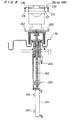
- FIGS. 9 and 10 show the rotary transporter
- FIG. 9 is a plan view of the rotary transporter
- FIG. 10 is a vertical cross-sectional view of the rotary transporter.
- the rotary transporters 27L and 27R have the same structure, and hence only the rotary transporter 27L will be described.
- the rotary transporter 27L for transporting the semiconductor wafer 101 has four wafer support stages 210 at angularly equal intervals of 90° , and each of the four wafer support stages 210 has six pins 201 standing on the stage for supporting the semiconductor wafer at six points.
- the semiconductor wafer can be supported by at least three pins, but in this embodiment, the six pins 201 are provided for supporting both of the semiconductor wafer having an orientation flat and the semiconductor wafer having a notch.
- a taper surface 202 having a taper angle of 15° to 25° from the perpendicular is formed at the forward end portion of the pin 201 to allow the semiconductor wafer to be centered when the semiconductor wafer is transferred.
- the wafer detecting sensors 200 are provided at positions spaced from the rotary transporter 27L.
- the sensor 200 is a photosensor comprising a light-emitting element 200a and a light-receiving element 200b, and is not moved with the stages of the rotary transporter 27L.
- the semiconductor wafer to be processed and the semiconductor wafer which has been processed are placed on each of the stages.
- Rinsing nozzles 501, 502, 503 and 504 for supplying a cleaning liquid to the semiconductor wafer are provided above or below the rotary transporter 27L and in the positions spaced from the rotary transporter 27L.
- the rinsing nozzles 501 to 504 are stationary and are not rotated with the stages. Pure water or ionic water is mainly used as a cleaning liquid.
- a separator 510 is provided on the rotary transporter 27L so as to separate the wafer support stages 210 from one another for preventing the slurry or the cleaning liquid used for cleaning the semiconductor wafer or the top ring from being scattered around.
- the rotary transporter 27L is coupled to a servomotor 511, and the semiconductor wafers on the rotary transporter 27L are transported by energizing the servomotor 511.
- a home position sensor 206 is provided on the lower portion of the rotary transporter 27L, and positioning of the wafer transfer position is controlled by the home position sensor 206 and the servomotor 511.
- the transfer positions which can be positioned are four positions at angular intervals of 90° with respect to the home position as a center.
- FIG. 9 shows the home position of the rotary transporter 27L.
- the rotary transporter 27L is rotated counterclockwise, and the stage 210 is located above the lifter 29.
- the rotary transporter 27R is rotated clockwise, and the stage 210 is located above the lifter 29.
- the semiconductor wafer 101 to be transferred to the top ring 32L is transferred to the reversing device 28L by the transfer robot 20.
- the semiconductor wafer 101 is held by the reversing device 28L, and then is reversed, i.e. turned upside down.
- the reversed semiconductor wafer 101 is received by the lifter 29L, and then lowered. While the semiconductor wafer 101 is lowered by the lifter 29L, the semiconductor wafer 101 is centered by the taper surfaces 202 of the pins 201 on the wafer support stage 210, and placed on the shoulder of the pins 201.
- the lifter 29L continues to be operated to cause the stage 260 to be lowered until the stage 260 does not interfere with the rotary transporter 27L even when the rotary transporter 27L is rotated. Thereafter, the rotary transporter 27L is rotated counterclockwise by an angle of 90 ° , and the semiconductor wafer 101 on the rotary transporter 27L is positioned above the pusher 30L. After positioning of the rotary transporter 27L is completed, the pusher 30L is operated to be raised, and the semiconductor wafer 101 is transferred to the top ring 32L located above the rotary transporter 27L.
- the semiconductor wafer 101 which has been polished by the top ring 32L is transferred to the wafer support stage 210 of the rotary transporter 27L located in advance below the top ring 32L by the pusher 30L.
- the semiconductor wafer 101 which has been received by the pusher 30L from the top ring 32L is placed on the shoulders of the pins 201 while the semiconductor wafer 101 is centered by the taper surfaces 202 of the pins 201.
- the semiconductor wafer 101 is placed on the wafer support stage 210, and the pusher 30L is lowered until the pusher 30L does not interfere with the rotary transporter 27L, and then the rotary transporter 27L is rotated couterclockwise by an angle of 90° to position the semiconductor wafer 101 above the lifter 29L.
- the lifter 29L is raised to receive the semiconductor wafer 101 from the wafer support stage 210 and to transfer the semiconductor wafer 101 to the reversing device 28L.
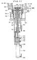
- FIG. 11, and FIGS. 12A through 12E show a pusher
- FIG. 11 is a vertical cross-sectional view of the pusher
- FIGS. 12A through 12E are views for explaining operation of the pusher.
- the pusher 30L and 30R have the same structure, and hence only the pusher 30L will be described.
- a guide stage 141 for holding the top ring is provided above a hollow shaft 140, and a spline shaft 142 is provided in the hollow shaft 140.
- a push stage 143 is provided above the spline shaft 142.
- An air cylinder 145 is coupled to the spline shaft 142 through a flexible joint 144. Two air cylinders are disposed vertically in series.
- the lower air cylinder 146 serves to lift and lower the guide stage 141 and the push stage 143, and lifts and lowers the hollow shaft 140 together with the air cylinder 145.
- the air cylinder 145 serves to lift and lower the push stage 143.
- a linear way 149 movable in directions of an X-axis and a Y-axis is provided to allow the top ring guide 148 to have an alignment mechanism.
- the guide stage 141 is fixed to the linear way 149, and the linear way 149 is fixed to the hollow shaft 140.
- the hollow shaft 140 is held by a bearing case 151 through a slide bush 150.
- the stroke of the air cylinder 146 is transmitted to the hollow shaft 140 through a compression spring 152.
- the push stage 143 is located above the guide stage 141, and a push rod 160 extending downwardly from the center of the push stage 143 passes through a slide bush 147 located at the center of the guide stage 141 to allow the push rod 160 to be centered.
- the push rod 160 contacts the upper end of the spline shaft 142.
- the push stage 143 is vertically moved by the air cylinder 145 through the spline shaft 142, so that the semiconductor wafer 101 is loaded on the top ring 32L.
- Compression springs 159 are provided at the peripheral portion of the push stage 143.
- top ring guides 148 are provided at the outer circumferential portion of the guide stage 141.
- Each of the top ring guides 148 has a two-step structure, the upper step 220 serves as a contact portion with the lower surface of the guide ring (retainer ring) 301, and the lower step 221 serves as a support portion for centering and supporting the semiconductor wafer 101.
- a taper surface having an angle of 25° to 35° from the perpendicular is formed at the upper step 220 for guiding the guide ring 301, and a tapered surface having an angle of 10° to 20° from the perpendicular is formed at the lower step 221 for guiding the semiconductor wafer 101.
- the top ring guides 148 receive the peripheral edge of the semiconductor wafer.
- a guide sleeve 153 is fixed to the guide stage 141 to prevent water from entering the central part of the guide stage 141 and to guide the guide stage 141 so that the guide stage 141 is returned to its original position.
- a center sleeve 154 located inside of the guide sleeve 153 is fixed to the bearing case 151 for centering the guide stage 141.
- the pusher is fixed to a motor housing 104 in the polishing section through the bearing case 151.
- a V-ring 155 is used to prevent water from entering between the push stage 143 and the guide stage 141, and has a lip held in contact with the guide stage 141 to prevent water from passing therethrough.
- the guide stage 141 is elevated, the volume of a portion G increases, thus lowering the pressure to thereby draw water.
- the V-ring 155 has a hole 202 defined in an inner side thereof to prevent the pressure from being lowered.
- a shock absorber 156 is provided for positioning of the top ring guides 148 in a vertical direction and for shock-absorbing when the top ring guides 148 contact the top ring 32L.
- upper and lower limit sensors are provided for detecting the position of the pusher in a vertical direction. That is, sensors 203 and 204 are provided on the air cylinder 145, and sensors 205 and 206 are provided on the air cylinder 146.
- a cleaning nozzle or nozzles for cleaning the pusher are provided to prevent the slurry attached to the pusher from contaminating the semiconductor wafer.
- a sensor for confirming the presence or absence of the semiconductor wafer on the pusher may be provided.
- the control of the air cylinders 145 and 146 are performed by double solenoid valves, respectively.
- the semiconductor wafer 101 is transported to a position above the pusher 30 by the rotary transporter 27L.
- the push stage 143 is raised by the air cylinder 145.
- the guide stage 141 and the components associated with the guide stage 141 are raised by the air cylinder 146. While the guide stage 141 is raised, the guide stage 141 passes through the wafer holding position of the rotary transporter 27L.
- the semiconductor wafer 101 is centered by the taper surfaces 207 of the top ring guides 148, and the pattern surface except peripheral portion of the semiconductor wafer is held by the push stage 143.
- the semiconductor wafer 101 is held by the push stage 143 at portions except for the peripheral edge thereof.
- top ring guides 148 are raised without being stopped, and the guide ring 301 is guided by the taper surfaces 208 of the top ring guides 148.
- the center of the top ring guides 148 is aligned with the center of the top ring 32 by the linear way 149 movable in X and Y directions, and the upper steps 220 of the top ring guides 148 contact the lower surface of the guide ring 301 and lifting of the guide stage 141 is stopped.
- the guide stage 141 is fixed and is not raised anymore.
- the air cylinder 146 continues to be actuated until the stopper fixed to the rod of the air cylinder 146 contacts the shock absorber 156, and hence only the spline shaft 142 continues to be raised because the compression spring 152 is compressed, and the push stage 143 is further raised.
- the push stage 143 holds the semiconductor wafer 101 at portions except for the peripheral edge of the semiconductor wafer 101, and transports the semiconductor wafer 101 to the top ring 32L. After the semiconductor wafer 101 contacts the top ring 32L, the lifting stroke of the air cylinder 146 is absorbed by the compression springs 159 to thereby protect the semiconductor wafer 101.
- the pusher After the top ring 32L completes the attraction of the semiconductor wafer 101, the pusher starts to be operated and the guide stage 141 and the push stage 143 are lowered to the position shown in FIG. 12A.
- the guide stage 141 When the guide stage 141 is lowered, the guide stage 141 is centered by the taper portion formed on the guide sleeve 153 and the taper portion formed on the center sleeve 154.
- the lowering of the guide stage 141 is completed, the operation of the loading of the semiconductor wafer is completed.
- the semiconductor wafer 101 is transported by the top ring 32L to a wafer unload position located above the pusher 30.
- the guide stage 141 and the components associated with the guide stage 141 are raised by the air cylinder 146, and the guide ring 301 of the top ring 32L is guided by the tapered surfaces 208 of the top ring guides 148.
- the center of the top ring guides 148 is aligned with the center of the top ring 32L by the linear way 149, and the upper steps 220 of the top ring guides 148 contact the lower surface of the guide ring 301 and the lifting of the guide stage 141 is stopped.
- the air cylinder 146 continues to be actuated until the stopper fixed to the rod of the air cylinder 146 contacts the shock absorber 156. However, since the upper steps 220 of the top ring guides 148 contact the lower surface of the guide ring 301 to cause the guide stage 141 to be fixed at this position, the air cylinder 146 pushes the spline shaft 142 together with the air cylinder 145 against urging force of the compression spring 152, thus lifting the push stage 143. At this time, as shown in FIG. 12E, the push stage 143 is not raised to a position higher than the wafer holding portion of the lower steps 221 of the top ring guides 148. In this embodiment, the air cylinder 146 is arranged to be further actuated after the top ring guides 148 contact the guide ring 301. The shock at this time is absorbed by the spring 152.
- the semiconductor wafer 101 is removed from the top ring 32L. At this time, the semiconductor wafer 101 is centered by the lower tapered surfaces 207 of the top ring guides 148, and the semiconductor wafer 101 is held by the lower steps 221 of the top ring guides 148 at the peripheral edge of the semiconductor wafer 101.
- the pusher starts to be operated to lower the guide stage 141. While the guide stage 141 is lowered, the guide stage 141 is centered by the guide sleeve 153 and the center sleeve 154. While the guide stage 141 is lowered, the semiconductor wafer 101 is transferred from the pusher 30 to the rotary transporter 27L. When the lowering of the guide stage 141 is completed, the operation of the unloading of the semiconductor wafer is completed.
- the pusher 30 since the pusher 30 has a centering mechanism for centering the main components of the pusher with respect to the top ring 32L, adjustment of the positional relationship between the pusher 30 and the top ring 32L can be easily performed.
- the lifting stroke of the push stage 143 is set to a position higher than the lower surface of the top ring 32L by about 2 mm, and thus positioning in a vertical direction can be easily performed. At this time, the shock of contact in the vertical direction can be absorbed by the spring.
- FIG. 13 is a schematic cross-sectional view showing the structure of the first polishing table and an arrangement of the optical sensor.
- the polishing tables 34L and 34R have the same structure, and thus only the polishing table 34L will be described below.
- an optical sensor 55 is embedded in the polishing table 34L.
- the optical sensor 55 is electrically connected to a controller 57 by a wire 59 extending through the polishing table 34L, a rotary connector (or slip ring) 56 mounted on an end of a polishing table support shaft.
- the controller 57 is connected to a display unit 58.
- FIG. 14 is a plan view of the polishing apparatus shown in FIG. 13.
- the optical sensor 55 is positioned so as to pass through the centers C W of the semiconductor wafers 101 held by all of the top rings 32L while the semiconductor wafers 101 are being polished, when the polishing table 34L rotates about its own axis C T . While the optical sensor 55 passes along an arcuate path beneath the semiconductor wafers 101, the optical sensor 55 continuously detects the thickness of an insulating layer such as a copper layer or the thickness of a conductive layer on the semiconductor wafer 101.
- an insulating layer such as a copper layer or the thickness of a conductive layer on the semiconductor wafer 101.
- the optical sensor 55 comprises a light-emitting element and a light-detecting element.
- the light-emitting element applies light to the surface, being polished, of the semiconductor wafer, and the light-detecting element detects reflected light from the surface, being polished, of the semiconductor wafer.
- the light-emitting element comprises a laser beam source or an LED.
- a portion of the light applied from the light-emitting element to the surface, being polished, of the semiconductor wafer passes through an uppermost layer such as a conductive layer or an insulating layer and is reflected from the surface of an underlayer under the uppermost layer. Therefore, the light-detecting element detects both the light reflected by the uppermost layer and the light reflected by the underlayer.
- a detected signal from the light-detecting element is processed by the controller 57 to detect the thickness of the uppermost layer such as the conductive layer or the insulating layer accurately.
- the principles of detecting the thickness of the layer by the optical sensor utilizes the interference of light caused by the top layer and a medium adjacent to the top layer.
- a part of the light is reflected from the surface of the thin layer while the remaining part of the light is transmitted through the thin layer.
- a part of the transmitted light is then reflected from the surface of the underlayer or the substrate, while the remaining part of the transmitted light is transmitted through the underlayer or the substrate.
- the underlayer is made of a metal, the light is absorbed in the underlayer.
- the phase difference between the light reflected from the surface of the thin layer and the light reflected from the surface of the underlayer or the substrate creates the interference.
- the light intensity is increased, while when the phases of the two lights are opposite to each other, the light intensity is decreased. That is, the reflection intensity varies with the wavelength of the incident light, the layer thickness, and the refractive index of the layer.
- the light reflected from the substrate is separated by a diffraction grating or the like, and a profile depicted by plotting the intensity of reflected light for each wavelength is analyzed to measure the thickness of the layer on the substrate.
- light is applied by the light-emitting element to the surfaces, being polished, of the three semiconductor wafers held by the respective top rings 32L one after another, each time the polishing table 34L makes one revolution, and the light reflected by the surfaces, being polished, of the semiconductor wafers is received by the light-detecting element.
- the light received by the light-detecting element is processed by the controller 57 to detect the thickness of the layer on the surface being polished.
- the thicknesses of the insulating layers or the metallic layers formed on the semiconductor wafers 101 held by all of the top rings 32L can be detected, as continuous measurements on a real-time basis, along a predetermined path extending from the outer circumferential edge to the center of each of the semiconductor wafers by the optical sensor 55.
- the thicknesses of the insulating layers or the metallic layers on all of the semiconductor wafers can be monitored at all times, and the end point of the CMP process can be accurately detected by detecting the following: The layer on the semiconductor wafer has been polished to a desired thickness; or the layer on the semiconductor wafer has been removed until the layer thickness has become zero.
- one or more optical sensors 55 may be added as indicated by an imaginary line in FIG. 14, so that at least two sensors are provided in the polishing table.
- an eddy-current sensor or the like may be provided to detect the thicknesses of the semiconductor wafers, in addition to the optical sensor, whereby the eddy-current sensor and the optical sensor may be selected depending on the measuring range of the thickness of the layer or the kind of layer to be measured.
- the polishing apparatus is such a multi-head type polishing apparatus which can polish a plurality of semiconductor wafers simultaneously, the end point of the CMP process in all of the semiconductor wafers during polishing can be detected.
- all of the semiconductor wafers can be uniformly polished without any irregularities in the polished state.
- each of the top rings is connected to the carousel 36L which is a single structural body, there is a possibility that the carousel 36L per se is inclined by the offset load. Therefore, in the present invention, when a plurality of the top rings 32L finish polishing operation individually, in order to reduce the offset load as much as possible, the following measures are taken: when polishing operation is terminated, the pressing force applied to the semiconductor wafer is set to zero and the pressing force applied to the retainer ring is left as it is; or the pressing force applied to the retainer ring is changed to such a pressing force as to be equal to the pressing force applied to the wafer during polishing plus the pressing force applied to the retainer ring during polishing. Next, the mechanism of the top ring which can apply the above retainer load will be described below.
- FIG. 15 is a schematic cross-sectional view showing the construction of the top ring of the present invention.
- the top ring 32L (or 32R) comprises a top ring body 80, and a holding plate 81 for holding a workpiece, to be polished, such as a semiconductor wafer 101.
- a chamber C is defined between the top ring body 80 and the holding plate 81, and is connected to a fluid source 82 through a regulator R 1 .
- An elastic pad 83 of polyurethane or the like is attached to the lower surface of the holding plate 81.
- a retainer ring (guide ring) 301 for holding the semiconductor wafer 101 on the lower surface, i.e.
- the wafer holding surface 81a of the holding plate 81 is disposed around the outer peripheral portion of the top ring 32L.
- a fluid pressure bag 85 comprising an annular tube is provided between the retainer ring 301 and the top ring 32L.
- the fluid pressure bag 85 is connected to the fluid source 82 through a regulator R 2 .
- a polishing table 34L (or 34R) having a polishing cloth 40 attached thereon is disposed below the top ring 32L.
- the polishing cloth 40 constitutes a polishing surface which is brought in sliding contact with the semiconductor wafer 101 for thereby polishing the semiconductor wafer 101.
- the top ring 32L is connected to a top ring shaft 46 through a ball 86.
- the top ring shaft 46 is connected to a fluid pressure cylinder 49 fixedly mounted on a top ring head 45.
- the fluid pressure cylinder 49 serves as an actuator for moving the top ring 32L vertically, and is connected to the fluid source 82 through a regulator R 3 .
- the top ring 32L presses the semiconductor wafer 101 to be polished against the polishing cloth 40 on the polishing table 34L under a certain pressing force F 1 for thereby polishing the semiconductor wafer 101.
- the pressing force F 1 is variable by regulating the regulator R 3 .
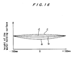
- FIG. 16 is a schematic view showing the configuration of the wafer holding surface 81a of the holding plate 81.
- the horizontal axis represents a distance (mm) from the center (O) of the holding plate 81
- the vertical axis represents a height of the wafer holding surface.
- alternate long and short dash line “d" shows the condition that the wafer holding surface 81a is flat. In this condition, no pressurized fluid is supplied to the chamber C, and the polishing pressure is not applied to the wafer holding surface 81a while polishing is not performed.
- the wafer holding surface 81a of the holding plate 81 is curved by a pressing force of the pressurized fluid in a convex shape in a downward direction as shown by the curve "a" in FIG. 16. That is, the wafer holding surface 81a defines a convex spherical surface. In this condition, the central portion of the semiconductor wafer 101 is pressed by the downwardly convex holding plate 81 against the polishing cloth 40 in a pressure higher than that applied onto the outer circumferential portion thereof.
- the regulator R 1 is controlled to reduce the pressure of the pressurized fluid supplied from the fluid source 82 to the chamber C or to stop the supply of the pressurized fluid to the chamber C, thereby making the wafer holding surface 81a of the holding plate 81 in the form of curve "b" or "c" shown in FIG. 16. Therefore, the polishing pressure applied to the central portion of the semiconductor wafer 101 is decreased and the polishing pressure applied to the outer circumferential portion of the semiconductor wafer 101 is increased, in comparison with the condition caused by the curve "a". Thus, insufficient polishing action at the outer circumferential portion of the semiconductor wafer can be corrected, and the entire surface of the semiconductor wafer 101 can be uniformly polished.
- the wafer holding surface 81a When the supply of the pressurized fluid to the chamber C is stopped, the wafer holding surface 81a is curved due to a polishing pressure in a slightly convex shape in an upward direction as shown by the curve "c". That is, the wafer holding surface 81a defines a concave spherical surface. If it is desirable to cause the wafer holding surface 81a of the holding plate 81 to curve upwardly in a higher degree than the condition shown by the curve "c", the chamber C may be evacuated by the fluid source 82 comprising a vacuum pump.
- the shape or configuration of the wafer holding surface 81a can be made downwardly convex (convex spherical surface) or upwardly convex (concave spherical surface) or flat by developing positive pressure (pressure higher than atmospheric pressure) or negative pressure (pressure lower than atmospheric pressure) in the chamber C.
- the wafer holding surface 81a of the holding plate 81 can be deformed in a desired shape by selecting material and thickness of the holding plate 81.
- Preferred materials to be selected for the holding plate are, in consideration of the environments in which the polishing apparatus is used, corrosion-resistant and elastic materials, for example, austenitic stainless steel (SUS 304, SUS 316, etc.), aluminium titan, or resin material such as polyphenylene sulfide (PPS) or polyethelethelketone (PEEK).
- Preferred thickness of the holding plate is, in consideration of the safety against the interior pressure of the chamber (preferably, not more than 0.1 MPa), in the range of 3 to 8 mm, and preferably about 5 mm in case of austenitic stainless steel. In case of other materials, the thickness should be selected on the basis of modulus of elasticity, while taking into consideration the safety.
- the retainer ring 301 presses the polishing cloth 40 under a pressing force F 2 by supplying a pressurized fluid such as a compressed air to the fluid pressure bag 85 from the fluid source 82.
- the pressing force F 1 exerted by the top ring 32L for pressing the semiconductor wafer 101 against the polishing cloth 40 on the polishing table 34L is variable
- the pressing force F 2 for pressing the retainer ring 301 against the polishing cloth 40 is also variable.
- These pressing forces F 1 , F 2 are variable independently of each other. Therefore, the pressing force F 2 which is applied to the polishing cloth 40 by the retainer ring 301 can be changed depending on the pressing force F 1 which is applied by the top ring 32L to press the semiconductor wafer 101 against the polishing cloth 40.
- the pressing force F 1 which is applied by the top ring 32L to press the semiconductor wafer 101 against the polishing cloth 40 is equal to the pressing force F 2 which is applied to the polishing cloth 40 by the retainer ring 301, then the distribution of applied polishing pressures, which result from a combination of the pressing forces F 1 , F 2 , is continuous and uniform from the center of the semiconductor wafer 101 to its peripheral edge and further to an outer circumferential edge of the retainer ring 301 disposed around the semiconductor wafer 101. Accordingly, the peripheral portion of the semiconductor wafer 101 is prevented from being polished excessively or insufficiently.
- FIGS. 17A through 17C schematically show how the polishing cloth 40 behaves when the relationship between the pressing force F 1 and the pressing force F 2 is varied.
- the pressing force F 1 is larger than the pressing force F 2 (F 1 >F 2 ).
- the pressing force F 1 is nearly equal to the pressing force F 2 (F 1 ⁇ F 2 ) .
- the pressing force F 1 is smaller than the pressing force F 2 (F 1 ⁇ F 2 ).
- the polishing pressure applied to the peripheral portion of the semiconductor wafer 101 is larger than the polishing pressure applied to the inner region of the semiconductor wafer 101, so that the amount of a material removed from the peripheral portion of the semiconductor wafer 101 is larger than the amount of a material removed from the inner region of the semiconductor wafer 101 while the semiconductor wafer 101 is being polished.
- the distribution of polishing pressures is continuous and uniform from the center of the semiconductor wafer 101 to its peripheral edge and further to the outer circumferential edge of the retainer ring 301, so that the amount of a material removed from the semiconductor wafer 101 is uniform from the peripheral edge to the inner region of the semiconductor wafer 101 while the semiconductor wafer 101 is being polished.
- the polishing pressure applied to the peripheral portion of the semiconductor wafer 101 is smaller than the polishing pressure applied to the inner region of the semiconductor wafer 101, so that the amount of a material removed from the peripheral edge of the semiconductor wafer 101 is smaller than the amount of a material removed from the inner region of the semiconductor wafer 101 while the semiconductor wafer 101 is being polished.
- fluid is supplied to the upper surface opposite to the wafer holding surface 81a of the holding plate 81 of the top ring 32L, and, at this time, the pressure of the fluid is properly selected in the range of positive pressure to negative pressure to thereby make the shape of the wafer holding surface 81a downwardly convex or upwardly convex.
- the semiconductor wafer 101 can be polished differently by varying the pressing force for pressing the semiconductor wafer 101 against the polishing cloth 40 at the outer circumferential portion and the central portion thereof. In some cases, the semiconductor wafer 101 is polished under the condition that the wafer holding surface 81a of the holding plate 81 is made flat.
- the pressing force F 2 of the retainer ring 301 disposed around the top ring 32L is determined on the basis of the pressing force F 1 of the top ring 32L, and the polishing is performed while the retainer ring 301 presses the polishing cloth 40 under the determined pressing force F 2 . That is, the polishing operation of the semiconductor wafer 101 is performed under the shape correcting effect of the wafer holding surface 81a by fluid having positive pressure or negative pressure as well as the shape correcting effect of the polishing cloth 40 by the retainer ring 301.
- irregularities of the polishing action can be sufficiently corrected and the localized area (for example, the central portion, the outer circumferential portion) of the semiconductor wafer 101 is prevented from being polished excessively or insufficiently.
- the pressing force F 1 for pressing the semiconductor wafer 101 against the polishing cloth 40 on the polishing table 34L by the top ring 34L becomes zero, and only the pressing force (retainer load) F 2 for pressing the polishing cloth 40 by the retainer ring 301 is applied.
- the pressing force of the retainer (retainer load) is equal to the pressing force F 2 which is applied during polishing, or the pressing force of the retainer is changed to such a pressing force as to be equal to the pressing force F 1 plus the pressing force F 2 .
- the offset load can be prevented from being applied to the polishing table 34L (or 34R) and the carousel 36L (or 36R).
- FIG. 18 is a cross-sectional view showing the scroll-type second polishing table
- FIG. 19A is a cross-sectional view taken along line P-P of FIG. 18,
- FIG. 19B is a cross-sectional view taken along line X-X of FIG. 19A.
- the second polishing tables 35L and 35R have the same structure, and hence only the polishing table 35L will be described.
- the scroll-type second polishing table 35L has an upper flange 751 of a motor 750, and a hollow shaft 752 connected to the upper flange 751 by bolts.
- a set ring 754 is supported by the upper portion of the shaft 752 through a bearing 753.
- a table 759 is fixed to the set ring 754, and a polishing table 755 is fixed to the table 759 by bolts 790.
- the polishing table 755 may comprise a grinding stone (fixed abrasive plate) entirely, or may comprise a plate made of a corrosion-resistant metal such as stainless steel and a polishing cloth attached to the plate.
- the polishing table 755 may have a flat upper surface or a slightly convex or concave upper surface.
- the shape of the upper surface of the polishing table 755 is selected depending on the kind of the semiconductor wafer 101 to be polished.
- the outer diameter of the polishing table 755 is set to a diameter having the diameter of the semiconductor wafer plus distance 2e (described below) or larger. That is, the diameter of the polishing table 755 is arranged such a diameter that when the polishing table 755 makes a translational motion, the semiconductor wafer does not project from the outer periphery of the polishing table 755.
- the translational motion may be called scroll motion or orbital motion.
- the set ring 754 has three or more supporting portions 758 in a circumferential direction, and the table 759 is supported by the supporting portions 758.
- a plurality of recesses 760, 761 are formed at positions corresponding to the upper surface of the supporting portions 758 and the upper end of the cylindrical member 795 at angularly equal intervals in a circumferential direction, and bearings 762 and 763 are mounted in the recesses 760 and 761.
- a support member 766 having two shafts 764 and 765 whose central axes are spaced by "e” is supported by the bearings 762 and 763. Specifically, the two shafts 764 and 765 are inserted into the bearings 762 and 763, respectively.
- the polishing table 755 makes a translational motion along a circle having a radius "e” by the motor 750.
- the center of the shaft 752 is off-centered by "e” from the center of the motor 750.
- a balancer 767 is fixed to the shaft 752 for providing a balance to the load caused by eccentricity.
- the supply of the abrasive liquid onto the polishing table 755 is conducted through the insides of the motor 750 and the shaft 752, a through-hole 757 provided at the central portion of the table 759, and a coupling 791.
- the supplied abrasive liquid is once stored in a space 756 defined between the polishing table 755 and the table 759, and then supplied to the upper surface of the polishing table 755 through a plurality of through-holes 768 formed in the polishing table 755.
- the number and position of the through-holes 768 can be selected depending on the kind of processes.
- the polishing cloth In the case where the polishing cloth is attached to the polishing table 755, the polishing cloth has through-holes at positions corresponding to the positions of the through-holes 768.
- the upper surface of the polishing table 755 In the case where the polishing table 755 is made of a grinding stone in entirety, the upper surface of the polishing table 755 has grid-like, spiral, or radial grooves, and the through-holes 768 may communicate with such grooves.
- the supplied abrasive liquid may be selected from pure water, chemicals, or slurry, and, if necessary, more than one kind of the abrasive liquid can be supplied simultaneously, alternatively, or sequentially.
- a flinger or a thrower 769 is attached to the table 759, and forms a labyrinth mechanism together with a trough 770.
- the upper and lower bearings 762, 763 are axially interconnected by the support member 766 comprising a cranked joint having the upper and lower shafts 764, 765 that are fitted respectively in the upper and lower bearings 762, 763.
- the shafts 764, 765 and hence the upper and lower bearings 762, 763 have respective axes horizontally spaced from each other by a distance "e".
- the cylindrical member 795 for supporting the lower bearing 763 is fixed to the frame, and hence is stationary.
- the shaft 752 When the motor 750 is energized, the shaft 752 is rotated by the radius of gyration (e) about the central axis of the motor 750, and thus the polishing table 755 makes a circulatory translational motion (scroll motion) through the cranked joint, and the semiconductor wafer 101 attached to the top ring 32L is pressed against a polishing surface of the polishing table 755.
- the semiconductor wafer 101 is polished by the abrasive liquid supplied through the through-hole 757, the space 756 and the through-holes 768.
- the semiconductor wafer 101 is polished by the relative circulatory translational motion having a radius "e" between the polishing surface of the polishing table 755 and the semiconductor wafer 101, and the semiconductor wafer 101 is uniformly polished over the entire surface of the semiconductor wafer. If a surface, to be polished, of the semiconductor wafer 101 and the polishing surface have the same positional relationship, then the polished semiconductor wafer is affected by a local difference in the polishing surface. In order to eliminate this influence, the top ring 32L is rotated at a low speed to prevent the semiconductor wafer from being polished at the same area on the polishing surface.
- the dressers 38L and 38R have the same structure, and hence only the dresser 38L will be described below.
- the dresser 38L is supported by a dresser head 60.
- the dresser head 60 is vertically movable by a dresser lifting/lowering air cylinder 64, and the dresser 38L is brought in contact with or away from the polishing surface on the polishing table 34L.
- a pulley 66 is fixed to an upper end of a rotating shaft 65 of the dresser 38L, and the pulley 66 is coupled to a pulley 69 connected to a rotating shaft 68 of a dresser motor 67 through a timing belt 70.
- the rotating shaft 68 of the dresser motor 67 and the pulley 69 are coupled by a key and a keyway so that the rotating shaft 68 and the pulley 69 are integrally rotated, but are vertically movable with respect to each other.
- the vertical movement of a supporting portion 78 for supporting the pulley 69 and the dresser head 60 is guided by a guide rail 79.
- the air cylinder 64 and the dresser motor 67 are supported by a housing 71, and the housing 71 is rotated by a swing motor 72.
- the swing motor 72 is fixed to a bracket 73.
- the bracket 73 engages with a guide rail 75 fixed to a base 74, and the bracket 73 is vertically slidable on the guide rail 75.
- a lifting/lowering air cylinder 76 is fixed to the bracket 73, and a forward end of a rod 76a of the lifting/lowering air cylinder 76 is fixed to the base 74.
- the base 74 is supported by the frame 77.
- the dresser 38L by actuating the lifting/lowering air cylinder 76, the dresser 38L, the dresser head 60, the dresser motor 67 and the swing motor 72 are integrally moved in a vertical direction. Therefore, in this dressing apparatus, when the dresser 38L is not used, the dresser 38L can retreat to a position below the polishing table 34L (or 34R). By energizing the swing motor 72, the dresser head 60 is swung to cause the dresser 38L to be positioned at the standby position and the dressing position on the polishing table.
- the lifting/lowering air cylinder 76 is actuated to cause the dresser 38L and the dresser head 60 to be raised. Then, the dresser 38L is moved to the dressing position on the polishing table by the swing motor 72. At this position, the dresser lifting/lowering air cylinder 64 is actuated, and the dresser 38L and the dresser head 60 are lowered for thereby pressing the dresser 38L against the polishing surface on the polishing table. At this time, the dresser 38L is rotated at a predetermined speed by the dresser motor 67. Further, the polishing table 34L (or 34R) is also rotated at a predetermined speed.
- the dresser for dressing the second polishing tables 35L, 35R comprises a conventional brush-type dresser.
- FIGS. 21A and 21B show the wafer station
- FIG. 21A is a front elevational view of the wafer station
- FIG. 21B is a side elevational view of the wafer station.
- FIG. 22A is a view of the wafer station as viewed in the direction indicated by the arrow I of FIG. 21A
- FIG. 22B is a view of the wafer station as viewed in the direction indicated by the arrow II of FIG. 21A
- FIG. 22C is a view of the wafer station as viewed in the direction indicated by the arrow III of FIG. 21A
- FIG. 22D is a view of the wafer station as viewed in the direction indicated by the arrow IV of FIG. 21A
- FIG. 22E is a view of the wafer station as viewed in the direction indicated by the arrow V of FIG. 21A.
- FIGS. 23A through FIG. 23C are views showing the manner in which the wafer station operates.
- the wafer station 90 comprises nine-stage of wafer trays T1 through T9 which are arranged in the descending order.
- the nine-stage of the wafer tray T1 to T9 are integrated into a single tray unit, and a plurality of posts (guide posts) 91 extending downwardly are provided at the lower portion of the single tray unit.
- a plurality of the posts 91 are vertically movably supported, through guides 93 each having a plain bearing therein, by a wafer station base 92 fixed to a cleaning base.
- the lower part of the tray unit and the upper surface of the wafer station base are coupled by a ball screw 94, and the ball screw 94 is rotated by a servomotor 95.
- the servomotor 95 By energizing the servomotor 95, the wafer tray is positionally fixed at a predetermined height.
- the nine-stage of the wafer trays T1 to T9 are arranged in the descending order as follows:
- the wafer trays T1, T2 and T3 accommodate dummy wafers which are used for running-in of a polishing pad on the polishing table.
- the three top rings 32L and the three top rings 32R correspond to the two polishing tables 34L and 34R, respectively.
- the dummy wafers R1 to R3 and L1 to L3 in the wafer trays T1, T2 and T3 are assigned to the respective three top rings 32L and 32R.
- a new dummy wafer should be replaced at a certain interval.
- new dummy wafers for replacement are accommodated in any one of four wafer cassettes, and such wafer cassette containing the dummy wafers therein is placed on the load-unload stage 2.
- the transfer robot 4 takes out a new dummy wafer for replacement from the wafer cassette, and the used dummy wafer in the wafer station 90 is replaced with the new dummy wafer for replacement.
- the transfer robot 4 takes out the dummy wafer placed on the wafer station 90 and places the dummy wafer on the wafer tray T4 one by one (in this case, the dummy wafer tray of the wafer station 90 is regarded just like a kind of wafer cassette). Thereafter, the transfer robot 20 and the transfer robot 21 transfer the respective dummy wafers from the wafer tray T4 to the respective rotary transporters 27L and 27R. After polishing of the dummy wafers, the dummy wafers are transferred to the cleaning apparatus 22 or 23, and to the cleaning apparatus 5 or 6, and then returned to the original positions of the wafer trays T1 to T3 by the transfer robots 20 and 21.
- the tray T4 serves as temporary placing positions, one of which is for placing the wafer R or L before polishing to be transferred from the transfer robot 4 to the transfer robot 20 (or 21), and the other of which is for placing the wafer R or L before polishing to be transferred from the transfer robot 21 (or 20) to the transfer robot 4.
- the wafer tray T5 for placing the wafers R1 and L1 after polishing and before cleaning (two wafers on the right and left side), the wafer tray T6 for placing the wafers R2 and L2 after polishing and before cleaning (two wafers on the right and left side), the wafer tray T7 for placing the wafer after a primary cleaning in the three-stage cleaning, R side ⁇ L side (one wafer), and the wafer tray T8 for placing the wafer after a primary cleaning in the three-stage cleaning, L side ⁇ R side (one wafer) will be described in the wafer processing routes (described later).
- the predetermined heights of the wafer trays T1 to T9 which are positionally fixed are set to three positions.
- the first position is the lowermost position of the tray unit.
- the transfer robot 4 can access the four-stage of the wafer trays, i.e. the wafer trays T1, T2 and T3 for dummy wafers and the wafer tray T4 for the wafers to be polished, and the transfer robots 20 and 21 can access the wafer tray T4 for the wafers to be polished.
- the second position is the intermediate height position of the tray unit.
- the transfer robots 20 and 21 can access the three-stage of wafer trays, i.e. the wafer tray T4 for the wafers to be polised and the wafer trays T5 and T6 for the wafers after polishing and before cleaning.
- the third position is the uppermost position of the tray unit.
- the transfer robot 20 and 21 can access the three-stage of wafer trays, i.e. the wafer trays T7 and T8 for the wafers after a primary cleaning in the three-stage cleaning and the wafer tray T9 for reservation.
- the transfer robot 4 cannot access the wafer trays of the wafer station 90 (there is no need to access).
- the wafer trays T5 to T8 (or T9), five faces are surrounded by a resin plate, except for a face through which the transfer robots 20 and 21 access the wafers.
- a shutter 401 which is vertically closable and openable by an air cylinder 400, and is opened only when the robot accesses the wafers.
- the wafer trays T5 to T8 are temporary placing positions for placing the wafers until the wafers which have been polished are transferred to a subsequent process
- nozzles 96 for spraying pure water or chemical liquid on the front and backside surfaces of the wafers so that the wafers are prevented from being dried, oxide films are prevented from being formed on the surfaces of the wafers by surrounding air, and the surfaces of the wafers are prevented from being etched by the polishing liquid or the cleaning liquid.
- sensors for detecting whether there is a semiconductor wafer or not in each of the wafer trays are provided.
- the first drain pipe is connected to the wafer tray T9 located at the lowermost position to serve as a draining pan for the whole wafer tray unit.
- the second drain pipe is attached to the lower portion of the wafer tray T8 to drain waste water from the wafer trays T7 and T8.
- the third drain pipe is connected to the lower portion of the wafer tray T6 to drain waste water from the wafer trays T5 and T6.
- the wafer trays T1 to T4 have no draining function because they are used in a dry atmosphere.
- the reason why the draining systems are separated in the manner descrived above is that if pure water or chemical liquid which is used in the wafer trays T7 and T8 for placing the wafers for the three stage cleaning and the wafer trays T5 and T6 for placing the wafers after polishing and before cleaning is different from each other, two kinds of chemical liquid are prevented from being mixed with each other or pure water and chemical liquid are prevented from being mixed with each other.
- the three drain pipes may be connected to a main drain pipe. Alternatively, depending on the kind of chemical liquid, the three drain pipes are separately connected to discrete plant drain utilities. Further, regarding chemical liquid treatment, the drain pipes may be connected to chemical liquid regeneration equipment or chemical liquid drain pipes in view of chemical properties. At this time, the same pipe may be used for chemical liquid having identical or similar chemical properties.
- the cleaning apparatuses 22 and 23 have a roll-shaped sponge rotatable about its own axis and pressed against a semiconductor wafer to clean the reverse side of the semiconductor wafer.
- the cleaning apparatuses 22 and 23 may have a roll type cleaning mechanism for rotating and pressing a roll-shaped sponge against the semiconductor wafer, or a pencil type cleaning mechanism for rotating and pressing a hemispherical sponge against the semiconductor wafer. Either one of the two types can be selected. Further, a megasonic type cleaning mechanism for cleaning the semiconductor wafer with a cleaning liquid to which ultrasonic vibration is applied may be added.
- the cleaning apparatuses 22 and 23 serve mainly to remove particles from the semiconductor wafers. Regardless of the type of the cleaning apparatus, each of the cleaning apparatuses can supply three or more kinds of cleaning liquid to the face (polished surface) and reverse sides of the semiconductor wafer.
- the cleaning liquid may comprise pure water.
- Each of the cleaning apparatuses 5 and 6 is capable of rinsing the reverse side of a semiconductor wafer.
- the cleaning apparatuses 5 and 6 may simultaneously conduct cleaning by the pencil type cleaning mechanism for rotating and pressing a hemispherical sponge against the semiconductor wafer and cleaning by the megasonic type cleaning mechanism for cleaning the semiconductor wafer with a cleaning liquid to which ultrasonic vibration is applied.
- Each of the cleaning apparatuses 5 and 6 can supply three or more kinds of cleaning liquid to the face (polished surface) and reverse sides of the semiconductor wafer.
- the cleaning liquid may comprise pure water.
- a stage for chucking a semiconductor wafer may be rotated at a high speed, and has a function for drying a cleaned wafer.
- each of the cleaning apparatuses may have cavitation jet type cleaning mechanism utilizing a cavitation effect in which a cavitation is applied to a cleaning liquid because it is as effective as the megasonic type.
- the cleaning apparatuses 5, 6, 22 and 23 have respective openings associated with respective shutters which can be opened only when the semiconductor wafers are to be introduced therein or removed therefrom.
- Each of the cleaning apparatuses 5, 6, 22 and 23 has a plurality of cleaning liquid supply lines associated with constant-rate flow valves that can be controlled by an air pressure. With the constant-rate flow valves combined with electropneumatic regulators for controlling the air pressure, the flow rate in the cleaning liquid supply lines can freely be established from a control panel. Cleaning liquids supplied to the cleaning apparatuses, and cleaning processes and cleaning time therefor can be set from the control panel.
- Guides are mounted on a base of the cleaning chamber (area B), and the cleaning apparatuses are mounted in the guides, so that the cleaning apparatuses can easily be replaced with different type cleaning apparatuses. There are provided positioning mechanisms for placing replaced cleaning apparatuses in the same position.
- Three wafers are sequentially taken out from the wafer cassette and transferred to the polishing table 34L to polish them.
- next three wafers are sequentially taken out from the wafer cassette and transferred to the polishing table 34R to polish them. After two sets of the three wafers are polished, they are transferred to the two cleaning apparatuses successively to conduct the two-stage cleaning.
- Three wafers are sequentially taken out from the wafer cassette and transferred to the polishing table 34L to polish them.
- next three wafers are sequentially taken out from the wafer cassette and transferred to the polishing table 34R to polish them.
- Three wafers are sequentially taken out from the wafer cassette and transferred to the polishing table 34L to conduct a primary polishing of the three wafers. After the primary polishing of the three wafers, the three wafers are transferred to the polishing table 34R to conduct a secondary polishing of the three wafers, and then the three wafers are transferred to the two cleaning apparatuses successively to conduct the two-stage cleaning.
- Three wafers are sequentially taken out from the wafer cassette and transferred to the polishing table 34L to conduct a primary polishing of the three wafers. After the primary polishing of the three wafers, the three wafers are transferred to the polishing table 34R to conduct a secondary polishing of the three wafers, and then the three wafers are transferred to the three cleaning apparatuses successively to conduct the three-stage cleaning.
- FIGS. 24 through 30 are schematic diagrams showing processes of the above parallel polishing and two-stage cleaning.
- three semiconductor wafers W1, W2 and W3 are processed successively in the following route: the wafer cassette 1 ⁇ the wafer station 90 (wafer tray T4) ⁇ the rotary transporter 27L ⁇ the polishing table 34L ⁇ the rotary transporter 27L. Thereafter, the wafer W1 is processed in the following route: the cleaning apparatus 22 ⁇ the cleaning apparatus 5 ⁇ the wafer cassette 1.
- the wafers W2 and W3 are processed in the following route: the wafer station 90 (wafer trays T5, T6) ⁇ the cleaning apparatus 22 ⁇ the cleaning apparatus 5 ⁇ the wafer cassette 1.
- the three wafers W4, W5 and W6 are processed in the following route: the wafer cassette 1 ⁇ the wafer station 90 (wafer tray T4) ⁇ the rotary transporter 27R ⁇ the polishing table 34R ⁇ the rotary transporter 27R. Thereafter, the wafer W4 is processed in the following route: the cleaning apparatus 23 ⁇ the cleaning apparatus 6 ⁇ the wafer cassette 1.
- the wafers W5 and W6 are processed in the following route: the wafer station 90 (wafer trays T5, T6) ⁇ the cleaning apparatus 23 ⁇ the cleaning apparatus 6 ⁇ the wafer cassette 1.
- FIGS. 31 through 37 are schematic diagrams showing processes of the above parallel polishing and three-stage cleaning.
- three semiconductor wafers W1, W2 and W3 are processed successively in the following route: the wafer cassette 1 ⁇ the wafer station 90 (wafer tray T4) ⁇ the rotary transporter 27L ⁇ the polishing table 34L ⁇ the rotary transporter 27L. Thereafter, the wafer W1 is processed in the following route: the cleaning apparatus 22 ⁇ the cleaning apparatus 5 ⁇ the wafer station 90 (wafer tray T8) ⁇ the cleaning apparatus 6 ⁇ the wafer cassette 1.
- the wafers W2 and W3 are processed in the following route: the wafer station 90 (wafer trays T5, T6) ⁇ the cleaning apparatus 22 ⁇ the cleaning apparatus 5 ⁇ the wafer station 90 (wafer trays T8) ⁇ the cleaning apparatus 6 ⁇ the wafer cassette 1.
- the three wafers W4, W5 and W6 are processed in the following route: the wafer cassette 1 ⁇ the wafer station 90 (wafer tray T4) ⁇ the rotary transporter 27R ⁇ the polishing table 34R ⁇ the rotary transporter 27R. Thereafter, the wafer W4 is processed in the following route: the cleaning apparatus 23 ⁇ the cleaning apparatus 6 ⁇ the wafer station 90 (wafer tray T7) ⁇ the cleaning apparatus 5 ⁇ the wafer cassette 1.
- the wafers W5 and W6 are processed in the following route: the wafer station 90 (wafer tray T4) ⁇ the cleaning apparatus 23 ⁇ the cleaning apparatus 6 ⁇ the wafer station 90 (wafer tray T7) ⁇ the cleaning apparatus 5 ⁇ the wafer cassette 1.
- FIGS. 38 through 47 are schematic diagrams showing processes of the above serial polishing and two-stage cleaning.
- three semiconductor wafers W1, W2 and W3 are processed successively in the following route: the wafer cassette 1 ⁇ the wafer station 90 (wafer tray T4) ⁇ the rotary transporter 27L ⁇ the polishing table 34L ⁇ the rotary transporter 27L. Thereafter, the wafer W1 is processed in the following route: the cleaning apparatus 22 ⁇ the wafer station 90 (wafer tray T8) ⁇ the rotary transporter 27R ⁇ the polishing table 34R ⁇ the rotary transporter 27R ⁇ the cleaning apparatus 23 ⁇ the cleaning apparatus 6 ⁇ the wafer cassette 1.
- the wafer W2 is processed in the following route: the wafer station 90 (wafer tray T5) ⁇ the cleaning apparatus 22 ⁇ the wafer station 90 (wafer tray T8) ⁇ the rotary transporter 27R ⁇ the polishing table 34R ⁇ the rotary transporter 27R ⁇ the wafer station 90 (wafer tray T5) ⁇ the cleaning apparatus 23 ⁇ the wafer station 90 (wafer tray T7) ⁇ the cleaning apparatus 5 ⁇ the wafer cassette 1.
- the wafer W3 is processed in the following route: the wafer station 90 (wafer tray T6) ⁇ the cleaning apparatus 22 ⁇ the wafer station 90 (wafer tray T8) ⁇ the rotary transporter 27R ⁇ the polishing table 34R ⁇ the rotary transporter 27R ⁇ the wafer station 90 (wafer tray T6) ⁇ the cleaning apparatus 23 ⁇ the cleaning apparatus 6 ⁇ the wafer cassette 1.
- FIGS. 48 through 58 are schematic diagrams showing processes of the above serial polishing and three-stage cleaning.
- three semiconductor wafers W1, W2 and W3 are processed successively in the following route: the wafer cassette 1 ⁇ the wafer station 90 (wafer tray T4) ⁇ the rotary transporter 27L ⁇ the polishing table 34L ⁇ the rotary transporter 27L. Thereafter, the wafer W1 is processed in the following route: the cleaning apparatus 22 ⁇ the wafer station 90 (wafer tray T8) ⁇ the rotary transporter 27R ⁇ the polishing table 34R ⁇ the rotary transporter 27R ⁇ the cleaning apparatus 23 ⁇ the cleaning apparatus 6 ⁇ the wafer station 90 (wafer tray T7) ⁇ the cleaning apparatus 5 ⁇ the wafer cassette 1.
- the wafers W2 and W3 are processed in the following route: the wafer station 90 (wafer trays T5, T6) ⁇ the cleaning apparatus 22 ⁇ the wafer station 90 (wafer tray T8) ⁇ the rotary transporter 27R ⁇ the polishing table 34R ⁇ the rotary transporter 27R ⁇ the wafer station 90 (wafer trays T5, T6) ⁇ the cleaning apparatus 23 ⁇ the cleaning apparatus 6 ⁇ the wafer station 90 (wafer tray T7) ⁇ the cleaning apparatus 5 ⁇ the wafer cassette 1.
Landscapes
- Engineering & Computer Science (AREA)
- Mechanical Engineering (AREA)
- Finish Polishing, Edge Sharpening, And Grinding By Specific Grinding Devices (AREA)
- Mechanical Treatment Of Semiconductor (AREA)
- Constituent Portions Of Griding Lathes, Driving, Sensing And Control (AREA)
- Grinding Of Cylindrical And Plane Surfaces (AREA)
Description
- The present invention relates to a polishing apparatus for polishing a workpiece such as a semiconductor wafer to a flat mirror finish, and more particularly to a multi-head type polishing apparatus having a plurality of top rings for holding workpieces with respect to a single polishing table.
- Recent rapid progress in semiconductor device integration demands smaller and smaller wiring patterns or interconnections and also narrower spaces between interconnections which connect active areas. One of the processes available for forming such interconnection is photolithography. The photolithographic process requires that surfaces on which pattern images are to be focused by a stepper should be as flat as possible because the depth of focus of the optical system is relatively small. It is therefore necessary to make the surfaces of semiconductor wafers flat for photolithography.
- One customary way of planarizing the surface of the semiconductor wafer is to polish the semiconductor wafer by a chemical mechanical polishing (CMP) process.
- There has been known a multi-head type polishing apparatus which has a plurality of top rings for holding semiconductor wafers with respect to a single polishing table and can polish a plurality of semiconductor wafers simultaneously. In this multi-head type polishing apparatus, semiconductor wafers are mounted on the respective top rings, and then all of the semiconductor wafers held by the top rings are simultaneously pressed against a polishing surface of the polishing table and polished. After polishing of the semiconductor wafers is conducted for a predetermined time, all of the top rings holding the semiconductor wafers are raised from the polishing table, and then all of the semiconductor wafers which have been polished are removed from the top rings. Thereafter, new semiconductor wafers are mounted on the top rings.
- In the conventional multi-head type polishing apparatus described above, a plurality of semiconductor wafers are simultaneously polished, and loading and unloading (i.e. replacement) of the semiconductor wafers are simultaneously conducted. However, in the case where loading of the semiconductor wafers to be polished on a plurality of top rings and unloading of the semiconductor wafers which have been polished from the top rings are automated, loading and unloading of the semiconductor wafers are necessary to be performed in a short time without a transfer error. However, in the multi-head type polishing apparatus, there has been no loading and unloading mechanism which can meet such requirements.
- The conventional multi-head type polishing apparatus is a dedicated polishing apparatus for conducting only polishing of semiconductor wafers, and hence the semiconductor wafers which have been polished are transported to a next cleaning process by a movable container in which they are immersed in water to keep them from drying during transportation. However, in the method in which the polishing process and the cleaning process are separately carried out, the cleanliness of a clean room tends to be impaired, and the polished semiconductor wafers need to be transported by an operator or a manually operated transportation means. Further, a large installation space is required for two kinds of apparatuses comprising the polishing apparatus and the cleaning apparatus that is used to carry out the subsequent cleaning process.
- Therefore, in order to make the polishing process clean and reduce the installation space of the apparatus, there has been demanded a multi-head type polishing apparatus which performs both a polishing process and a cleaning process therein and is of a dry-in and dry-out type for introducing semiconductor wafers therein in a dry condition and removing polished and cleaned semiconductor wafers therefrom in a dry condition.
- Further, attention is drawn to U.S. Patent 5,329,732, which shows a polishing apparatus having a multi-head comprising a polishing table, a plurality of top rings (carriers) attached to a polishing assembly, a rotary transporter (index table) and a plurality of pushers for transferring workpieces between said index table and said carriers. To allow transfer of substrates between the carriers and respective cups of the index table, the polishing assembly as a whole is moved along a linear rail from a position above the polishing table to a position above the index table. After transfer of the substrates the polishing assembly is again moved as a whole back to a position above the polishing table. During polishing of the substrates each wafer carrier is oscillated by a polish arm attached to the polishing assembly.
- It is therefore an object of the present invention to provide a multi-head type polishing apparatus which can be used as a dry-in and dry-out type polishing apparatus, has a high processing capability per unit time and unit installation area for processing workpieces such as semiconductor wafers.
- In accordance with the present invention, a polishing apparatus as set forth in
claim 1 is provided. Further embodiments of the invention are claimed in the dependent claims. - In particular, there is provided a polishing apparatus having a multi-head, comprising: a polishing table having a polishing surface; a plurality of top rings for holding workpieces and pressing the workpieces against the polishing surface; a carousel for supporting the top rings and indexing the top rings; a rotary transporter disposed in a position which can be accessed by the top rings and having a plurality of portions positioned on a predetermined circumference from a center of rotation of the rotary transporter for holding the workpieces, the rotary transporter having an indexing function for indexing the plurality of portions; and a pusher for transferring the workpieces between the rotary transporter and the top rings, wherein each of said top rings is connected to said carousel through a swing arm, and is angularly movable by said swing arm to a polishing position on said polishing table and a loading and unloading position on said rotary transporter.
- According to the present invention, it is possible to shorten the time required to transfer workpieces to be polished, such as semiconductor wafers, to the top rings for thereby greatly increasing the number of processed workpieces per unit time, i.e., throughput.
- The above and other objects, features, and advantages of the present invention will be apparent from the following description when taken in conjunction with the accompanying drawings which illustrates preferred embodiments of the present invention by way of example.
-
- FIG. 1 is a plan view showing a layout of various components of a polishing apparatus;
- FIG. 2 is a plan view showing polishing units on the left and right sides in which three top rings perform different operations;
- FIG. 3 is vertical cross-sectional view showing the relationship between the multi-head type top rings supported by the carousel and the polishing table;
- FIG. 4 is a perspective view showing the relationship between the carousel, the top ring swing arms and the top rings by removing a support member and posts;
- FIG. 5 is a perspective view showing the relationship between the carousel, the top ring swing arms and the multi-head type top rings by removing the support member and the posts;
- FIG. 6 is a plan view of a guide plate;
- FIG. 7A is a plan view of a reversing device;
- FIG. 7B is a side elevational view, partly in cross section, of the reversing device;
- FIG. 8 is a vertical cross-sectional view of a lifter;
- FIG. 9 is a plan view of a rotary transporter;
- FIG. 10 is a vertical cross-sectional view of the rotary transporter;
- FIG. 11 is a vertical cross-sectional view of a pusher;
- FIGS. 12A through 12E are vertical cross-sectional views illustrative of the manner in which the pusher operates;
- FIG. 13 is a schematic cross-sectional view showing a construction of a first polishing table and an arrangement of an optical sensor;
- FIG. 14 is a plan view of the polishing apparatus shown in FIG. 13;
- FIG. 15 is a schematic cross-sectional view showing the structure of the top ring;
- FIG. 16 is a graph showing the configuration of the wafer holding surface of the holding plate of the top ring;
- FIGS. 17A, 17B, and 17C are enlarged fragmentary vertical cross-sectional views showing the behavior of a polishing cloth when the relationship between a pressing force applied by a top ring and a pressing force applied by a retainer ring is varied;
- FIG. 18 is a vertical cross-sectional view of a scroll-type polishing table;
- FIG. 19A is a cross-sectional view taken along line P - P of FIG. 18;
- FIG. 19B is a cross-sectional view taken along line X - X of FIG. 19A;
- FIG. 20 is a front view of a dresser for dressing the polishing table;
- FIG. 21A is a front view of a wafer station;
- FIG. 21B is a side view of the wafer station;
- FIG. 22A is a view of the wafer station as viewed in the direction indicated by the arrow I of FIG. 21A;
- FIG. 22B is a view of the wafer station as viewed in the direction indicated by the arrow II;
- FIG. 22C is a view of the wafer station as viewed in the direction indicated by the arrow III;
- FIG. 22D is a view of the wafer station as viewed in the direction by the arrow IV;
- FIG. 22E is a view of the wafer station as viewed in the direction by the arrow V;
- FIGS. 23A through 23C are views illustrative of the manner in which the wafer station operates;
- FIG. 24 is a diagram illustrative of a wafer processing route in the polishing apparatus shown in FIGS. 1 though 23;
- FIG. 25 is a diagram illustrative of the wafer processing route in the polishing apparatus shown in FIGS. 1 though 23;
- FIG. 26 is a diagram illustrative of the wafer processing route in the polishing apparatus shown in FIGS. 1 though 23;
- FIG. 27 is a diagram illustrative of the wafer processing route in the polishing apparatus shown in FIGS. 1 though 23;
- FIG. 28 is a diagram illustrative of the wafer processing route in the polishing apparatus shown in FIGS. 1 though 23;
- FIG. 29 is a diagram illustrative of the wafer processing route in the polishing apparatus shown in FIGS. 1 though 23;
- FIG. 30 is a diagram illustrative of the wafer processing route in the polishing apparatus shown in FIGS. 1 though 23;
- FIG. 31 is a schematic diagram illustrative of an example of a process of parallel polishing and three-stage cleaning;
- FIG. 32 is a schematic diagram illustrative of the example of the process of parallel polishing and three-stage cleaning;
- FIG. 33 is a schematic diagram illustrative of the example of the process of parallel polishing and three-stage cleaning;
- FIG. 34 is a schematic diagram illustrative of the example of the process of parallel polishing and three-stage cleaning;
- FIG. 35 is a schematic diagram illustrative of the example of the process of parallel polishing and three-stage cleaning;
- FIG. 36 is a schematic diagram illustrative of the example of the process of parallel polishing and three-stage cleaning;
- FIG. 37 is a schematic diagram illustrative of the example of the process of parallel polishing and three-stage cleaning;
- FIG. 38 is a schematic diagram illustrative of an example of a process of serial polishing and two-stage cleaning;
- FIG. 39 is a schematic diagram illustrative of the example of the process of serial polishing and two-stage cleaning;
- FIG. 40 is a schematic diagram illustrative of the example of the process of serial polishing and two-stage cleaning;
- FIG. 41 is a schematic diagram illustrative of the example of the process of serial polishing and two-stage cleaning;
- FIG. 42 is a schematic diagram illustrative of the example of the process of serial polishing and two-stage cleaning;
- FIG. 43 is a schematic diagram illustrative of the example of the process of serial polishing and two-stage cleaning;
- FIG. 44 is a schematic diagram illustrative of the example of the process of serial polishing and two-stage cleaning;
- FIG. 45 is a schematic diagram illustrative of the example of the process of serial polishing and two-stage cleaning;
- FIG. 46 is a schematic diagram illustrative of the example of the process of serial polishing and two-stage cleaning;
- FIG. 47 is a schematic diagram illustrative of the example of the process of serial polishing and two-stage cleaning;
- FIG. 48 is a schematic diagram illustrative of an example of a process of serial polishing and three-stage cleaning;
- FIG. 49 is a schematic diagram illustrative of the example of the process of serial polishing and three-stage cleaning;
- FIG. 50 is a schematic diagram illustrative of the example of the process of serial polishing and three-stage cleaning;
- FIG. 51 is a schematic diagram illustrative of the example of the process of serial polishing and three-stage cleaning;
- FIG. 52 is a schematic diagram illustrative of the example of the process of serial polishing and three-stage cleaning;
- FIG. 53 is a schematic diagram illustrative of the example of the process of serial polishing and three-stage cleaning;
- FIG. 54 is a schematic diagram illustrative of the example of the process of serial polishing and three-stage cleaning;
- FIG. 55 is a schematic diagram illustrative of the example of the process of serial polishing and three-stage cleaning;
- FIG. 56 is a schematic diagram illustrative of the example of the process of serial polishing and three-stage cleaning;
- FIG. 57 is a schematic diagram illustrative of the example of the process of serial polishing and three-stage cleaning; and
- FIG. 58 is a schematic diagram illustrative of the example of the process of serial polishing and three-stage cleaning.
- A polishing apparatus according to embodiments of the present invention will be described below.
- FIG. 1 shows a layout of various components of a polishing apparatus. As shown in FIG. 1, a polishing apparatus comprises four load-unload
stages 2 each for placing awafer cassette 1 which accommodates a plurality of semiconductor wafers. The load-unloadstage 2 may have a mechanism for raising and lowering thewafer cassette 1. Atransfer robot 4 having two hands is provided onrails 3 so that thetransfer robot 4 can move along therails 3 and access therespective wafer cassettes 1 on the respective load-unloadstages 2. - The
transfer robot 4 has two hands which are located in a vertically spaced relationship, and the lower hand is used only for taking out a semiconductor wafer from thewafer cassette 1 and the upper hand is used only for returning the semiconductor wafer to thewafer cassette 1. This arrangement allows that a clean semiconductor wafer which has been cleaned is placed at an upper side and is not contaminated. The lower hand is a vacuum attraction-type hand for holding a semiconductor wafer under vacuum, and the upper hand is a recess support-type hand for supporting a peripheral edge of a semiconductor wafer by a recess formed on the hand. The vacuum attraction-type hand can hold a semiconductor wafer and transport the semiconductor wafer even if the semiconductor wafer is not located at a normal position in the wafer cassette due to a slight displacement, and the recess support-type hand can transport a semiconductor wafer while keeping the semiconductor wafer clean because dust is not collected unlike the vacuum attraction-type hand. - Two
cleaning apparatuses wafer cassettes 1 with respect to therails 3 of thetransfer robot 4. Thecleaning apparatuses transfer robot 4. Between the twocleaning apparatuses transfer robot 4, there is provided awafer station 90 having multi-stage wafer supports (wafer trays) in a vertical direction. Thecleaning apparatuses - An area B in which the
cleaning apparatuses wafer station 90 are disposed and an area A in which thewafer cassettes 1 and thetransfer robot 4 are disposed are partitioned by apartition wall 14 so that the cleanliness of the area B and the area A can be separated. Thepartition wall 14 has an opening for allowing semiconductor wafers to pass therethrough, and a shutter 11 is provided at the opening of thepartition wall 14. Atransfer robot 20 having two hands is disposed at a position where thetransfer robot 20 can access thecleaning apparatus 5 and thewafer station 90, and atransfer robot 21 having two hands is disposed at a position where thetransfer robot 21 can access thecleaning apparatus 6 and thewafer station 90. - The
transfer robot 20 and thetransfer robot 21 have the respective two hands which are located in a vertically spaced relationship. The respective upper hands of thetransfer robot 20 and thetransfer robot 21 are used for transporting a semiconductor wafer which has been cleaned to the cleaning apparatuses or wafer trays of thewafer station 90, and the respective lower hands of thetransfer robot 20 and thetransfer robot 21 are used for transporting a semiconductor wafer which has not cleaned or a semiconductor wafer to be polished. Since the lower hand is used to transfer a semiconductor wafer to or from a reversing device, the upper hand is not contaminated by drops of a rinsing water which fall from an upper wall of the reversing device. - A
cleaning apparatus 22 is disposed at a position adjacent to thecleaning apparatus 5 and accessible by the hands of thetransfer robot 20, and anothercleaning apparatus 23 is disposed at a position adjacent to thecleaning apparatus 6 and accessible by the hands of thetransfer robot 21. - All the cleaning
apparatuses wafer station 90, and thetransfer robots apparatuses - The polishing apparatus has a
housing 100 for enclosing various components therein. The interior of thehousing 100 is partitioned into a plurality of compartments or chambers (including the areas A and B) bypartitions - A polishing chamber separated from the area B by the
partition wall 24 is formed, and is further divided into two areas C and D by thepartition wall 25. In each of the two areas C and D, there are provided two polishing tables, and a carousel having three top rings for holding a semiconductor wafer and pressing the semiconductor wafer against the polishing tables. That is, the polishing tables 34L and 35L are provided in the area C, and the polishing tables 34R and 35R are provided in the area D. Further, thecarousel 36L is provided in the area C and thecarousel 36R is provided in the area D. - An abrasive liquid nozzle (not shown) for supplying an abrasive liquid to the polishing table 34L and a
dresser 38L for dressing the polishing table 34L are disposed in the area C. An abrasive liquid nozzle (not shown) for supplying an abrasive liquid to the polishing table 34R and adresser 38R for dressing the polishing table 34R are disposed in the area D. Adresser 39L for dressing the polishing table 35L is disposed in the area C, and adresser 39R for dressing the polishing table 35R is disposed in the area D. As shown in FIG. 1, the polishing units disposed on the left and right sides are disposed in line symmetry with respect to thepartition wall 25. The both polishing units have the respective threetop rings - As shown in FIG. 1, in the area C separated from the area B by the
partition wall 24 and at a position that can be accessed by the hands of thetransfer robot 20, there is provided a reversingdevice 28L for reversing a semiconductor wafer, and in the area D and at a position that can be accessed by the hands of thetransfer robot 21, there is provided a reversingdevice 28R for reversing a semiconductor wafer. Thepartition wall 24 between the area B and the areas C, D has two openings each for allowing semiconductor wafers to pass therethrough, one of which is used for transferring the semiconductor wafer to or from the reversingdevice 28L and the other of which is used for transferring the semiconductor wafer to or from the reversingdevice 28R.Shutters partition wall 24. The reversingdevices transfer robot 20 transfers a semiconductor wafer to the reversingdevice 28L, and thetransfer robot 21 transfers a semiconductor wafer to the reversingdevice 28R. - A
rotary transporter 27L is disposed in the area C for transferring semiconductor wafers between the reversingdevice 28L and the threetop ring 32L supported by thecarousel 36L. Therotary transporter 27L has four stages for placing a semiconductor wafer at angularly equal intervals, and can hold a plurality of semiconductor wafers thereon at the same time. The semiconductor wafer which has been transported to the reversingdevice 28L is transferred to therotary transporter 27L by actuating alifter 29L disposed below therotary transporter 27L when the center of the stage of therotary transporter 27L is aligned with the center of the semiconductor wafer held by the reversingdevice 28L. The semiconductor wafer placed on the stage of therotary transporter 27L is transported to a position above apusher 30L by the indexing motion of therotary transporter 27L. At this time, thetop ring 32L is located at a position above therotary transporter 27L (loading and unloading position) beforehand by a swing motion thereof. The semiconductor wafer is transferred from therotary transporter 27L to thetop ring 32L by actuating thepusher 30L disposed below therotary transporter 27L when the center of thetop ring 32L is aligned with the center of the semiconductor wafer placed on the stage of therotary transporter 27L. - By repeating the above operation, the semiconductor wafers are sequentially loaded on the three
top rings 32L supported by thecarousel 36L. - The semiconductor wafer transferred to the
top ring 32L is held under vacuum by a vacuum attraction mechanism of thetop ring 32L, and transported to the polishing table 34L. Thereafter, the semiconductor wafer is polished by a polishing surface comprising a polishing cloth or a grinding stone (or a fixed abrasive plate) attached on the polishing table 34L. The second polishing tables 35L is disposed at a position that can be accessed by the top rings 32L when thetop ring 32L is located at an accessible position to the second polishing table 35L. With this arrangement, a primary polishing of the semiconductor wafer can be conducted by the polishing table 34L, and then a secondary polishing of the semiconductor wafer can be conducted by the second polishing table 35L. In this case, a buffing polishing of the semiconductor wafer can be conducted by the second polishing table 35L. - A
rotary transporter 27R is disposed in the area D for transferring semiconductor wafers between the reversingdevice 28R and the threetop ring 32R supported by thecarousel 36R. Therotary transporter 27R has four stages for placing a semiconductor wafer at angularly equal intervals, and can hold a plurality of semiconductor wafers thereon at the same time. The semiconductor wafer which has been transported to the reversingdevice 28R is transferred to therotary transporter 27R by actuating alifter 29R disposed below therotary transporter 27R when the center of the stage of therotary transporter 27R is aligned with the center of the semiconductor wafer held by the reversingdevice 28R. The semiconductor wafer placed on the stage of therotary transporter 27R is transported to a position above apusher 30R by the indexing motion of therotary transporter 27R. At this time, thetop ring 32R is located at a position above therotary transporter 27R (loading and unloading position) beforehand by a swing motion thereof. The semiconductor wafer is transferred from therotary transporter 27R to thetop ring 32R by actuating thepusher 30R disposed below therotary transporter 27R when the center of thetop ring 32R is aligned with the center of the semiconductor wafer placed on the stage of therotary transporter 27R. - By repeating the above operation, the semiconductor wafers are sequentially loaded on the three
top rings 32R supported by thecarousel 36R. - The semiconductor wafer transferred to the
top ring 32R is held under vacuum by a vacuum attraction mechanism of thetop ring 32R, and transported to the polishing table 34R. Thereafter, the semiconductor wafer is polished by a polishing surface comprising a polishing cloth or a grinding stone (or a fixed abrasive plate) attached on the polishing table 34R. The second polishing tables 35R is disposed at a position that can be accessed by the top rings 32R when thetop ring 32R is located at an accessible position to the second polishing table 35R. With this arrangement, a primary polishing of the semiconductor wafer can be conducted by the polishing table 34R, and then a secondary polishing of the semiconductor wafer can be conducted by the second polishing table 35R. In this case, a buffing polishing of the semiconductor wafer can be conducted by the second polishing table 35R. - In both of the polishing units, after a semiconductor wafer is polished by the first polishing table 34L or 34R and before the
top ring top ring top ring - After the semiconductor wafer is polished by the first polishing surface of the first polishing table 34L or 34R and the second polishing surface of the second polishing table 35L or 35R, the first and second polishing surfaces are dressed by the
dressers - In the polishing unit on the left side, the semiconductor wafer which has been polished is transferred from the
top ring 32L to thepusher 30L, and then transferred from thepusher 30L to therotary transporter 27L by lowering thepusher 30L. Thereafter, the semiconductor wafer is transported to a position below the reversingdevice 28L by the indexing motion of therotary transporter 27L, and then returned to the reversingdevice 28L by raising thelifter 29L. - In the polishing unit on the right side, the semiconductor wafer which has been polished is transferred from the
top ring 32R to thepusher 30R, and then transferred from thepusher 30R to therotary transporter 27R by lowering thepusher 30R. Thereafter, the semiconductor wafer is transported to a position below the reversingdevice 28R by the indexing motion of therotary transporter 27R, and then returned to the reversingdevice 28R by raising thelifter 29R. - The semiconductor wafer returned to the reversing
device top ring top ring rotary transporter - FIG. 2 shows the polishing units on the left and right sides in which the three
top rings top ring 32L-1 is located in the loading and unloading position, thetop ring 32L-2 is located in the overhanging position with respect to the polishing table 34L, and thetop ring 32L-3 is located on the second polishing table 35L. In the polishing unit on the right side, thetop ring 32R-1 accesses the loading and unloading position, thetop ring 32R-2 accesses the polishing table 35R, and thetop ring 32R-3 is located away from the polishing table 34R. Other components or devices are in the same condition as those in FIG. 1. - Further, the
dressers dressers dressers dressers - FIGS. 3 through 5 show the relationship between multi-head type top rings 32L (or 32R) supported by the
carousel 36L (or 36R) and the polishing table 34L (or 34R). FIG. 3 is a schematic side view and FIGS. 4 and 5 are schematic perspective views. Thecarousels top rings carousel 36L, the top rings 32L and the polishing table 34L on the left side will be described. - As shown in FIG. 3, the
carousel 36L is supported by asupport member 42 which is supported by a plurality of posts 41 (in FIG. 3, only one post is shown). Thecarousel 36L is supported from thesupport member 42 by amain shaft 43 which is rotatable. Themain shaft 43 is coupled to amotor 44 fixed to thesupport member 42. Therefore, thecarousel 36L is rotatable about a vertical axis O by rotating themain shaft 43. Thecarousel 36L supports three top ring swing arms 45 (in FIG. 3, only one swing arm is shown). Each of the topring swing arms 45 has an L shaped structure. Each of the topring swing arms 45 is coupled to amotor 48 through a decelerator 47. By energizing themotor 48, the topring swing arm 45 is swung with respect to thecarousel 36L. The topring swing arm 45 supports thetop ring 32L at its forward end. Thetop ring 32L is coupled to an air cylinder (not shown) through atop ring shaft 46, and thetop ring shaft 46 is coupled to amotor 51 through atiming belt 50. Therefore, thetop ring 32L is vertically movable by the air cylinder (not shown), and rotatable about its own axis by themotor 51. - FIGS. 4 and 5 show the relationship between the
carousel 36L, the topring swing arms 45 and the top rings 32 by removing thesupport member 42 and theposts 41. As shown in FIGS. 4 and 5, thecarousel 36L comprises three heads h1, h2 and h3 which extend radially outwardly from themain shaft 43 at angularly equal intervals of 120° . Further, the topring swing arm 45 supported by each of the heads h1, h2 and h3 of thecarousel 36L has an L shaped structure, and the base portion of theswing arm 45 is supported by thecarousel 36L and the forward end of theswing arm 45 supports thetop ring 32L. - On the right side in FIGS. 3 through 5, the
rotary transporter device lifter pusher device rotary transporter lifter rotary transporter pusher rotary transporter - In FIG. 3, one of the
top rings 32L is located above therotary transporter 27L. In FIG. 4, the threetop rings 32L are located on the polishing table 34L to polish three semiconductor wafers, simultaneously. At this time, the topring swing arms 45 are swung radially inwardly so that the topring swing arms 45 are located inside thecarousel 36L. In FIG. 5, thetop ring 32L-1 is located above the loading and unloading position where thetop ring 32L-1 is located above therotary transporter 27L, thetop ring 32L-2 is in an overhanging position with respect to the polishing table 34L, and thetop ring 32L-3 is located on the second polishing table 35L to perform a buffing polishing of the semiconductor wafer which has been polished on the polishing table 34L. In FIG. 5, the topring swing arms 45 are swung so that the topring swing arms 45 are radially outwardly opened from thecarousel 36L. In FIG. 5, thetop rings 32L are shown by adding reference numerals to distinguish the respective top rings. - Next, the function of the support member, the carousel and the top ring swing arm will be further described.
- The
support member 42 is securely supported by the threeposts 41 vertically extending from atable base 52. A jack comprising a gear box composed of a worm gear, a servo motor and a ball screw is provided at each of the threeposts 41. The three jacks are synchronously controlled, and simultaneously operated to raise thecarousel 36L at the time of maintenance such as replacement of the polishing cloth attached to the polishing table 34L (or 34R). - In the normal operation, the
support member 42 is supported by the threeposts 41 vertically extending from thetable base 52, and thesupport member 42 is stationary in such a state that a coupling projection provided on the top end of the post and a coupling recess provided on the bottom of the support member engage with each other. Further, in order to ensure the coupling of the coupling projection and the coupling recess, the motor of the jack is energized to generate torque which is then applied to the coupling, thus creating such a state like bolt tighting. - Further, in order to supply pressurized fluid, electric power and signals to the
carousel 36L (or 36R), pipes and wires are spirally arranged on thesupport member 42 so that the rotation of thecarousel 36L (or 36R) does not cause breaking of wires or twisting of the pipes. - The
carousel 36L (or 36R) is supported by themotor 44 which has a firm bearing therein and is fixed to thesupport member 42. Thecarousel 36L is controlled so as to be rotatable only when the topring swing arms 45 are located at the polishing position. When thecarousel 36L (or 36R) is not rotated, thecarousel 36L (or 36R) is held so as not to be rotated by an air brake housed therein. The air brake is released only when thecarousel 36L (or 36R) is rotated. Thecarousel 36L is rotatable in clockwise and counterclockwise directions, and the rotation of thecarousel 36L is limited to an angle of 240° . That is, thecarousel 36L does not continue to be rotated in the same direction. Themotor 44 for rotating thecarousel 36L is thin, and large in diameter as in the motor for rotating the polishing table, and is rotatable at a low speed. Themain shaft 43 for supporting thecarousel 36L is a hollow shaft for allowing pressurized fluid, electric power and control signals to be supplied to thecarousel 36L and the topring swing arms 45. - Each of the top
ring swing arms 45 is supported by thecarousel 36L (or 35R) through a firm bearing, and is capable of swinging in a horizontal plane. The topring swing arm 45 is capable of swinging, rotating and moving, in combination with rotating angle of the carousel, for thereby being located at the following positions: the polishing position on the polishing table 34L (or 34R); the overhanging position in which the semiconductor wafer projects from the outer periphery of the polishing table in order to allow the polished semiconductor wafer to be easily removed from the polishing pad; the buffing position in which the semiconductor wafer held by thetop ring 32L (or 32R) is pressed against the polishing table 35L (or 35R); the loading and unloading position in which the semiconductor wafer is mounted on thetop ring 32L (or 32R) or the semiconductor wafer is removed from thetop ring 32L (or 32R); and the maintenance position in which thetop ring 32L (or 32R) is detached from the top ring shaft (splined shaft) 46. The swinging, rotating and moving of the topring swing arm 45 is controlled by aservomotor 48 attached to thecarousel 36L (or 36R) through a firm bearing. A sensor and a mechanical stopper are provided at a swing end of the swinging and rotating of the topring swing arm 45. - Further, when the top
ring swing arm 45 is located at the polishing position on the polishing table 34L (or 34R), a part of the topring swing arm 45 is located inside thecarousel 36L (or 36R), and further another part of the topring swing arm 45 is brought in contact with a plate attached to the bottom surface of the carousel so that the topring swing arm 45 is prevented from moving upwardly. Further, the upper surface of the topring swing arm 45 is pressed against the plate by an air cylinder attached to the bottom surface of the carousel. With this arrangement, the topring swing arm 45 is prevented from being elastically deformed upwardly for thereby keeping its posture stably. - From a fool proof standpoint, a
guide plate 53 for guiding the top ring swing arm is provided on the bottom surface of thesupport member 42 so that the topring swing arm 45 is not erroneously operated at positions other than the positions where the topring swing arm 45 is allowed to be operated. Further, aguide pole 56 is fixed to the upper surface of the topring swing arm 45, and is fitted into a groove formed in the guide plate 53 (described later). Thus, theguide pole 56 is configured such that theguide pole 56 is not movable along a route other than the route which is predetermined on theguide plate 53. - Next, the
guide plate 53 will be described in detail. FIG. 6 is a plan view of theguide plate 53. As shown in FIG. 6, sixarcuate grooves 54a to 54f are formed in theguide plate 53. Thegroove 54a is a groove for limiting the loading and unloading position, agroove 54b is a groove for limiting the maintenance position, thegroove 54c is a groove for limiting the standby position, thegroove 54d is a groove for limiting the top ring replacement position, thegroove 54e is a groove for limiting the buffing position, and thegroove 54f is a groove for limiting the maintenance position. Theguide poles 56 vertically provided on the respective topring swing arms 45 are fitted in thesegrooves 54a to 54f, and hence the movements of the respective topring swing arms 45 are limited. Further, sensors are provided at essential positions of the routes defined by theguide plate 53, and hence if the respective topring swing arms 45 tend to be moved beyond the predetermined routes, interlocking is worked by a control circuit. - In the above structure, a batch processing of three semiconductor wafers will be described. In this case, operation of the polishing unit on the left side will be described.
- The semiconductor wafer transferred to the reversing
device 28L by thetransfer robot 20 is transferred to therotary transporter 27L by actuating thelifter 29L disposed below therotary transporter 27L when the center of the stage of therotary transporter 27L is aligned with the center of the semiconductor wafer held by the reversingdevice 28L. The semiconductor wafer placed on the stage of therotary transporter 27L is transported to a position below thetop ring 32L by the indexing motion of therotary transporter 27L. At this time, thetop ring 32L is located at the loading and unloading position of therotary transporter 27L by the swing motion of the topring swing arm 45. The semiconductor wafer is transferred from therotary transporter 27L to thetop ring 32L by actuating thepusher 30L disposed below therotary transporter 27L when the center of thetop ring 32L is aligned with the center of the semiconductor wafer placed on the stage of therotary transporter 27L. - By repeating the above operation, the semiconductor wafer is loaded on the three
top rings 32L supported by thecarousel 36L. - After the semiconductor wafers are loaded on all of the top rings 32L, the three semiconductor wafers are simultaneously polished by pressing the semiconductor wafers against the polishing table 34L. In this case, the semiconductor wafers are pressed against a polishing cloth or a grinding stone attached to the rotating polishing table 34L by the air cylinder (not shown). At this time, the abrasive liquid is supplied from the abrasive liquid nozzle, and the semiconductor wafer is polished in the presence of the abrasive liquid between the lower surface of the semiconductor wafer and the polishing surface. During this polishing, all of the semiconductor wafers are monitored by an optical sensor (described later) to detect a polished condition of the semiconductor wafers.
- After a predetermined time of polishing, the
top ring 32L holds the semiconductor wafer under vacuum. Thereafter, the semiconductor wafer held by thetop ring 32L is moved toward the outer periphery of the polishing table 34L by the swing motion of the topring swing arm 45 while the semiconductor wafer contacts the polishing cloth on the polishing table. Finally, the semiconductor wafer projects from the outer periphery of the polishing table 34L in such a manner that the center of the semiconductor wafer is located on the polishing table 34L and near the periphery of the polishing table 34L as much as possible and about 40% of the surface of the semiconductor wafer projects from the polishing table 34L. Thereafter, the air cylinder (not shown) is actuated, and thetop ring 32L holding the semiconductor wafer is raised. Depending on the polishing cloth which is used, the surface tension between the slurry on the polishing cloth and the semiconductor wafer may be stronger than the attractive force of the top ring, tending to leave the semiconductor wafer on the polishing cloth. In order to reduce the surface tension, the semiconductor wafer is allowed to project from the polishing table and then thetop ring 32L is raised. If more than 40 % of the surface area of the semiconductor wafer projects from the polishing table, then the top ring would be tilted, causing the semiconductor wafer to hit the edge of the polishing table and hence to crack. It is therefore preferable for the semiconductor wafer to project about 40 % of its surface area from the polishing table. In other words, it is essential that the center of the semiconductor wafer is located on the polishing table 34L. - When lifting of the
top ring 32L is completed, the sensor detects the completion of the lifting action of the air cylinder (not shown). Thereafter, thetop ring 32L starts to be swung, and is moved to the position above thepusher 30L and transfers the semiconductor wafer to thepusher 30L. After the semiconductor wafer is removed from thetop ring 32L, a cleaning liquid is supplied to the lower surface of thetop ring 32L from a nozzle or nozzles located below thetop ring 32L, and the wafer holding surface of thetop ring 32L and surrounding regions are cleaned. The supply of the cleaning liquid may continue to prevent the top ring from drying until a subsequent semiconductor wafer is transferred to thetop ring 32L. The cleaning liquid may be intermittently supplied to the top ring in view of the running cost. During polishing, the polishing time may be divided into a plurality of steps, and the pressing force of the top ring, the rotational speed of the top ring and the holding method of the semiconductor wafer may be changed for each of the steps. Further, the kind, the amount, the concentration, the temperature, the supply timing, and like of the abrasive liquid used may be varied. - Next, the rotary transporter and associated devices thereof will be described with reference to FIGS. 7 through 12.
- FIGS. 7A and 7B show the reversing device, and FIG. 7A is a plan view of a reversing device and FIG. 7B is a side elevational view, partly in cross section, of the reversing device. Since the reversing
devices device 28L will be described below. As shown in FIGS. 7A and 7B, the reversingdevice 28L has a pair ofarcuate arms 230 supporting a plurality of (e.g., six)pins 231 fixed thereto which have grooves for clamping a semiconductor wafer therein. Thearms 230 can be opened and closed in response to movement of ashaft 234 that can be pushed and pulled by anair cylinder 232 and acompression spring 233. When theair cylinder 232 is extended, thearms 230 are opened thereby. When theair cylinder 232 is contracted, thearms 230 are closed under the force of thecompression spring 233. Theshaft 234 and a tip end of theair cylinder 232 are spaced from each other by a distance, and theshaft 234 is pulled back until astopper 235 contacts anend block 236 under the bias of thecompression spring 233. - The
end block 236 is adjusted such that when asemiconductor wafer 101 is chucked, a clearance of 1 mm is created between thestopper 235 and theend block 236. Thestopper 235 has a slit defined therein, and a transmissiontype light sensor 237 is positioned to detect light that has passed through the slit when thesemiconductor wafer 101 is clamped by thearms 230. Therefore, when thesemiconductor wafer 101 is not clamped or cannot be clamped properly, the transmissiontype light sensor 237 does not detect light. Therefore, the transmissiontype light sensor 237 is capable of recognizing whether thesemiconductor wafer 101 is present or not in the reversing device 28. - A slide mechanism for the
shaft 234 and apulley 238 are connected to each other, and thepulley 238 is coupled to apulley 240 fixed to a shaft end of a steppingmotor 239 through abelt 241. When the steppingmotor 239 is energized, thearms 230 are rotated about a horizontal axis. - As shown in FIG. 1, the
shutters devices transfer robots shutters transfer robots transfer robots shutters - Next, the operation of the reversing device will be described with reference to FIGS. 7A and 7B.
- The
transfer robot 20 and thelifter 29L can access the reversingdevice 28L and transfer the semiconductor wafer to the reversingdevice 28L. Thetransfer robot 21 and thelifter 29R can access the reversingdevice 28R and transfer the semiconductor wafer to the reversingdevice 28R. - The reversing
device 28L waits for the semiconductor wafer which is conveyed by thetransfer robot 20 or thelifter 29L in such a state that thearms 230 are opened. Thearms 230 are closed when the semiconductor wafer conveyed by the lower hand of thetransfer robot 20 or thelifter 29L is positioned in the same vertical height as wafer holding grooves ofpins 231 fixed to thearms 230 and the center of the semiconductor wafer is substantially positioned at the center of the pin arrangement on thearms 230 and after a signal indicative of completion of movement from thetransfer robot 20 or thelifter 29L is generated. After the presence of thesemiconductor wafer 101 is confirmed by asensor 237, the hand of thetransfer robot 20 is lowered to a certain height and is then retracted. Alternatively, after the presence of thesemiconductor wafer 101 is confirmed by thesensor 237, thelifter 29L is lowered. In this manner, thesemiconductor wafer 101 is transferred from thetransfer robot 20 or thelifter 29L to the reversingdevice 28L. Thesemiconductor wafer 101 transferred to the reversingdevice 28L is reversed by actuating thearms 230 with the steppingmotor 239. The reversedsemiconductor wafer 101 is kept in the same condition until thetransfer robot 20 or thelifter 29L accesses the reversing device 28 to receive the semiconductor wafer therefrom. - The reversing operation of the semiconductor wafer is carried out before and after polishing of the semiconductor wafer. In case of reversing the
semiconductor wafer 101 which has been polished, in order to prevent abrasive liquid or ground-off particles attached to thesemiconductor wafer 101 during polishing from being dried on thesemiconductor wafer 101, thesemiconductor wafer 101 is rinsed by a cleaning liquid during or after reversing of the semiconductor wafer. The cleaning liquid used to rinse thesemiconductor wafer 101 comprises pure water or a chemical liquid, and is applied from spray nozzles at a required rate under a required pressure at an optimum angle for a desired period of time. The rinsing process enables a subsequent cleaning process to be conducted in a sufficient cleaning performance. While thesemiconductor wafer 101 is waiting on the reversingdevice 28L, the cleaning liquid continues to be supplied to thesemiconductor wafer 101. However, in view of the running cost, the cleaning liquid may be supplied intermittently to reduce its amount in use. - While the reversing
device 28L is not clamping thesemiconductor wafer 101, the grooves for clamping thesemiconductor wafer 101 and surrounding areas thereof may be cleaned by the cleaning liquid to prevent thesemiconductor wafer 101 from being contaminated by members that will contact thesemiconductor wafer 101. - FIG. 8 is a vertical cross-sectional view of the lifter. The
lifter lifter 29L will be described. Thelifter 29L comprises astage 260 for placing a semiconductor wafer thereon and anair cylinder 261 for lifting and lowering thestage 260. Theair cylinder 261 and thestage 260 are coupled by ashaft 262 which is vertically movable. Thestage 260 has threesupport portions 263 disposed at angularly equal intervals in a circumferential direction and extending radially outwardly. The threesupport portions 263 are arranged in the angularly equal intervals so that the semiconductor wafer having an orientation flat can be held and are reliably transported. The threesupport portions 263 are disposed at positions where they are not aligned with thepins 231 for chucking the semiconductor wafer in the reversingdevice 28L. That is, the first peripheral edge of the semiconductor wafer held by thepins 231 does not correspond to the second peripheral edge of the semiconductor wafer held by thesupport portions 263 of thelifter 29L. Thewafer support portions 263 of thelifter 29L which performs the transfer of the semiconductor wafer to the reversingdevice 28L or therotary transporter 27L have respective support surfaces for supporting the semiconductor wafer thereon, and respective taper surfaces extending radially outwardly and upwardly from the support surfaces for centering the semiconductor wafer when the semiconductor wafer is placed on the support surfaces. - The wafer support surfaces of the
stage 260 is raised by actuation of theair cylinder 261 to a position where the semiconductor wafer is held by the reversingdevice 28L. A stopper 264 having a shock absorbing function is provided to stop raising of thestage 260. When astopper base 265 fixed to theshaft 262 contacts the stopper 264, further actuation of theair cylinder 261 is stopped, and the lifting of thestage 260 fixed to theshaft 262 is simultaneously stopped. By adjusting the location of the stopper 264, the lifting height of thestage 260 can be adjusted to a transfer position of the semiconductor wafer between thelifter 29L and the reversingdevice 28L.Sensors air cylinder 261 to detect completion of lifting and lowering of theair cylinder 261, respectively. - Next, the operation of the lifter having the above structure will be described. The
lifter 29L constitutes a wafer transfer mechanism for transferring the semiconductor wafer between the reversingdevice 28L and therotary transporter 27L. The semiconductor wafer to be polished is transferred from thetransfer robot 20 to the reversingdevice 28L. Thereafter, the semiconductor wafer is reversed by the reversingdevice 28L to cause a pattern surface (the surface on which semiconductor device is formed) of the semiconductor wafer to face downward. Thestage 260 of thelifter 29L is raised toward the semiconductor wafer held by the reversingdevice 28L and is stopped immediately below the semiconductor wafer. When thesensor 266 provided on theair cylinder 261 detects the stop of thelifter 29L at a position where thestage 260 is located immediately below the semiconductor wafer, the reversingdevice 28L releases the semiconductor wafer by opening thearms 230 and the semiconductor wafer is placed on thestage 260 of thelifter 29L. Thereafter, thelifter 29L is lowered while holding the semiconductor wafer thereon. While the semiconductor wafer is lowered by thelifter 29L, the semiconductor wafer is transferred to therotary transporter 27L. At this time, the semiconductor wafer is placed on the pins of therotary transporter 27L. After the semiconductor wafer is transferred to therotary transporter 27L, thelifter 29L continues to be operated to lower thestage 260, and then is stopped when thestage 260 is lowered by the stroke of theair cylinder 261. - The semiconductor wafer which has been polished is transferred from the
rotary transporter 27L to the reversingdevice 28L by thelifter 29L. That is, the semiconductor wafer which has been polished is transported by therotary transporter 27L to the position above thelifter 29L. At this time, thestage 260 of thelifter 29L is located immediately below therotary transporter 27L. After it is confirmed that the semiconductor wafer placed on therotary transporter 27L is located at the position immediately above thestage 260 of thelifter 29L and the movement of the semiconductor wafer is stopped, thestage 260 of thelifter 29L starts to be raised. Thestage 260 of thelifter 29L receives the semiconductor wafer from therotary transporter 27 while thestage 260 is lifted. Thereafter, thestage 260 of thelifter 29L continues to be lifted. At this time, the reversingdevice 28L waits for the semiconductor wafer in such a state that thearms 230 are opened to be ready for cramping the semiconductor wafer. The lifting of the semiconductor wafer is stopped at the position where the semiconductor wafer is horizontally aligned with the wafer holding grooves of thepins 231 on thearms 230. The completion of lifting of thestage 260 in thelifter 29L is detected by thesensor 266 provided on theair cylinder 261, and the detecting signal by thesensor 266 is sent to a controller of the polishing apparatus to allow the controller to recognize the completion of lifting of thestage 260. When the controller of the polishing apparatus receives the detecting signal, the reversingdevice 28L is operated to close thearms 230. By this operation, the semiconductor wafer is held by the reversingdevice 28L. After it is confirmed that the semiconductor wafer is held by the reversingdevice 28L, thestage 260 of thelifter 29L is lowered. - FIGS. 9 and 10 show the rotary transporter, and FIG. 9 is a plan view of the rotary transporter and FIG. 10 is a vertical cross-sectional view of the rotary transporter. The
rotary transporters rotary transporter 27L will be described. As shown in FIGS. 9 and 10, therotary transporter 27L for transporting thesemiconductor wafer 101 has four wafer support stages 210 at angularly equal intervals of 90° , and each of the four wafer support stages 210 has sixpins 201 standing on the stage for supporting the semiconductor wafer at six points. The semiconductor wafer can be supported by at least three pins, but in this embodiment, the sixpins 201 are provided for supporting both of the semiconductor wafer having an orientation flat and the semiconductor wafer having a notch. Ataper surface 202 having a taper angle of 15° to 25° from the perpendicular is formed at the forward end portion of thepin 201 to allow the semiconductor wafer to be centered when the semiconductor wafer is transferred. - The
wafer detecting sensors 200 are provided at positions spaced from therotary transporter 27L. Thesensor 200 is a photosensor comprising a light-emitting element 200a and a light-receiving element 200b, and is not moved with the stages of therotary transporter 27L. The semiconductor wafer to be processed and the semiconductor wafer which has been processed are placed on each of the stages. - Rinsing
nozzles rotary transporter 27L and in the positions spaced from therotary transporter 27L. The rinsingnozzles 501 to 504 are stationary and are not rotated with the stages. Pure water or ionic water is mainly used as a cleaning liquid. Aseparator 510 is provided on therotary transporter 27L so as to separate the wafer support stages 210 from one another for preventing the slurry or the cleaning liquid used for cleaning the semiconductor wafer or the top ring from being scattered around. Therotary transporter 27L is coupled to aservomotor 511, and the semiconductor wafers on therotary transporter 27L are transported by energizing theservomotor 511. Ahome position sensor 206 is provided on the lower portion of therotary transporter 27L, and positioning of the wafer transfer position is controlled by thehome position sensor 206 and theservomotor 511. The transfer positions which can be positioned are four positions at angular intervals of 90° with respect to the home position as a center. - Next, the operation of the
rotary transporter 27L having the above structure will be described. FIG. 9 shows the home position of therotary transporter 27L. Therotary transporter 27L is rotated counterclockwise, and thestage 210 is located above thelifter 29. Therotary transporter 27R is rotated clockwise, and thestage 210 is located above thelifter 29. - The
semiconductor wafer 101 to be transferred to thetop ring 32L is transferred to the reversingdevice 28L by thetransfer robot 20. Thesemiconductor wafer 101 is held by the reversingdevice 28L, and then is reversed, i.e. turned upside down. The reversedsemiconductor wafer 101 is received by thelifter 29L, and then lowered. While thesemiconductor wafer 101 is lowered by thelifter 29L, thesemiconductor wafer 101 is centered by the taper surfaces 202 of thepins 201 on thewafer support stage 210, and placed on the shoulder of thepins 201. After thesemiconductor wafer 101 is placed on thepins 201, thelifter 29L continues to be operated to cause thestage 260 to be lowered until thestage 260 does not interfere with therotary transporter 27L even when therotary transporter 27L is rotated. Thereafter, therotary transporter 27L is rotated counterclockwise by an angle of 90° , and thesemiconductor wafer 101 on therotary transporter 27L is positioned above thepusher 30L. After positioning of therotary transporter 27L is completed, thepusher 30L is operated to be raised, and thesemiconductor wafer 101 is transferred to thetop ring 32L located above therotary transporter 27L. - The
semiconductor wafer 101 which has been polished by thetop ring 32L is transferred to thewafer support stage 210 of therotary transporter 27L located in advance below thetop ring 32L by thepusher 30L. Thesemiconductor wafer 101 which has been received by thepusher 30L from thetop ring 32L is placed on the shoulders of thepins 201 while thesemiconductor wafer 101 is centered by the taper surfaces 202 of thepins 201. Thesemiconductor wafer 101 is placed on thewafer support stage 210, and thepusher 30L is lowered until thepusher 30L does not interfere with therotary transporter 27L, and then therotary transporter 27L is rotated couterclockwise by an angle of 90° to position thesemiconductor wafer 101 above thelifter 29L. After positioning of therotary transporter 27L is completed, thelifter 29L is raised to receive thesemiconductor wafer 101 from thewafer support stage 210 and to transfer thesemiconductor wafer 101 to the reversingdevice 28L. - FIG. 11, and FIGS. 12A through 12E show a pusher, and FIG. 11 is a vertical cross-sectional view of the pusher and FIGS. 12A through 12E are views for explaining operation of the pusher. The
pusher pusher 30L will be described. - As shown in FIG. 11, a
guide stage 141 for holding the top ring is provided above ahollow shaft 140, and aspline shaft 142 is provided in thehollow shaft 140. Apush stage 143 is provided above thespline shaft 142. Anair cylinder 145 is coupled to thespline shaft 142 through a flexible joint 144. Two air cylinders are disposed vertically in series. Thelower air cylinder 146 serves to lift and lower theguide stage 141 and thepush stage 143, and lifts and lowers thehollow shaft 140 together with theair cylinder 145. Theair cylinder 145 serves to lift and lower thepush stage 143. - A
linear way 149 movable in directions of an X-axis and a Y-axis is provided to allow thetop ring guide 148 to have an alignment mechanism. Theguide stage 141 is fixed to thelinear way 149, and thelinear way 149 is fixed to thehollow shaft 140. Thehollow shaft 140 is held by abearing case 151 through aslide bush 150. The stroke of theair cylinder 146 is transmitted to thehollow shaft 140 through acompression spring 152. - The
push stage 143 is located above theguide stage 141, and apush rod 160 extending downwardly from the center of thepush stage 143 passes through aslide bush 147 located at the center of theguide stage 141 to allow thepush rod 160 to be centered. Thepush rod 160 contacts the upper end of thespline shaft 142. Thepush stage 143 is vertically moved by theair cylinder 145 through thespline shaft 142, so that thesemiconductor wafer 101 is loaded on thetop ring 32L. Compression springs 159 are provided at the peripheral portion of thepush stage 143. - Three top ring guides 148 are provided at the outer circumferential portion of the
guide stage 141. Each of the top ring guides 148 has a two-step structure, theupper step 220 serves as a contact portion with the lower surface of the guide ring (retainer ring) 301, and thelower step 221 serves as a support portion for centering and supporting thesemiconductor wafer 101. A taper surface having an angle of 25° to 35° from the perpendicular is formed at theupper step 220 for guiding theguide ring 301, and a tapered surface having an angle of 10° to 20° from the perpendicular is formed at thelower step 221 for guiding thesemiconductor wafer 101. When thesemiconductor wafer 101 is unloaded from the top ring, the top ring guides 148 receive the peripheral edge of the semiconductor wafer. - A
guide sleeve 153 is fixed to theguide stage 141 to prevent water from entering the central part of theguide stage 141 and to guide theguide stage 141 so that theguide stage 141 is returned to its original position. Acenter sleeve 154 located inside of theguide sleeve 153 is fixed to thebearing case 151 for centering theguide stage 141. The pusher is fixed to amotor housing 104 in the polishing section through thebearing case 151. - A V-
ring 155 is used to prevent water from entering between thepush stage 143 and theguide stage 141, and has a lip held in contact with theguide stage 141 to prevent water from passing therethrough. When theguide stage 141 is elevated, the volume of a portion G increases, thus lowering the pressure to thereby draw water. In order to prevent water from being drawn, the V-ring 155 has ahole 202 defined in an inner side thereof to prevent the pressure from being lowered. - A
shock absorber 156 is provided for positioning of the top ring guides 148 in a vertical direction and for shock-absorbing when the top ring guides 148 contact thetop ring 32L. In each of theair cylinders sensors air cylinder 145, andsensors air cylinder 146. A cleaning nozzle or nozzles for cleaning the pusher are provided to prevent the slurry attached to the pusher from contaminating the semiconductor wafer. A sensor for confirming the presence or absence of the semiconductor wafer on the pusher may be provided. The control of theair cylinders - Next, the operation of the pusher having the above structure will be described below.
- As shown in FIG. 12A, the
semiconductor wafer 101 is transported to a position above the pusher 30 by therotary transporter 27L. When the top ring 32 is located in a loading position above the pusher 30 and does not hold the semiconductor wafer, as shown in FIG. 12B, thepush stage 143 is raised by theair cylinder 145. When the completion of raising of thepush stage 143 is detected by thesensor 203, as shown in FIG. 12C, theguide stage 141 and the components associated with theguide stage 141 are raised by theair cylinder 146. While theguide stage 141 is raised, theguide stage 141 passes through the wafer holding position of therotary transporter 27L. At this time, thesemiconductor wafer 101 is centered by the taper surfaces 207 of the top ring guides 148, and the pattern surface except peripheral portion of the semiconductor wafer is held by thepush stage 143. Thesemiconductor wafer 101 is held by thepush stage 143 at portions except for the peripheral edge thereof. - While the
push stage 143 holds the semiconductor wafer, the top ring guides 148 are raised without being stopped, and theguide ring 301 is guided by the taper surfaces 208 of the top ring guides 148. The center of the top ring guides 148 is aligned with the center of the top ring 32 by thelinear way 149 movable in X and Y directions, and theupper steps 220 of the top ring guides 148 contact the lower surface of theguide ring 301 and lifting of theguide stage 141 is stopped. - When the
upper steps 220 of the top ring guides 148 contact the lower surface of theguide ring 301, theguide stage 141 is fixed and is not raised anymore. However, theair cylinder 146 continues to be actuated until the stopper fixed to the rod of theair cylinder 146 contacts theshock absorber 156, and hence only thespline shaft 142 continues to be raised because thecompression spring 152 is compressed, and thepush stage 143 is further raised. At this time, as shown in FIG. 12D, thepush stage 143 holds thesemiconductor wafer 101 at portions except for the peripheral edge of thesemiconductor wafer 101, and transports thesemiconductor wafer 101 to thetop ring 32L. After thesemiconductor wafer 101 contacts thetop ring 32L, the lifting stroke of theair cylinder 146 is absorbed by the compression springs 159 to thereby protect thesemiconductor wafer 101. - After the
top ring 32L completes the attraction of thesemiconductor wafer 101, the pusher starts to be operated and theguide stage 141 and thepush stage 143 are lowered to the position shown in FIG. 12A. When theguide stage 141 is lowered, theguide stage 141 is centered by the taper portion formed on theguide sleeve 153 and the taper portion formed on thecenter sleeve 154. When the lowering of theguide stage 141 is completed, the operation of the loading of the semiconductor wafer is completed. - The
semiconductor wafer 101 is transported by thetop ring 32L to a wafer unload position located above the pusher 30. When the wafer unload stage of therotary transporter 27L is located above the pusher 30 and does not hold the semiconductor wafer, theguide stage 141 and the components associated with theguide stage 141 are raised by theair cylinder 146, and theguide ring 301 of thetop ring 32L is guided by the taperedsurfaces 208 of the top ring guides 148. The center of the top ring guides 148 is aligned with the center of thetop ring 32L by thelinear way 149, and theupper steps 220 of the top ring guides 148 contact the lower surface of theguide ring 301 and the lifting of theguide stage 141 is stopped. Theair cylinder 146 continues to be actuated until the stopper fixed to the rod of theair cylinder 146 contacts theshock absorber 156. However, since theupper steps 220 of the top ring guides 148 contact the lower surface of theguide ring 301 to cause theguide stage 141 to be fixed at this position, theair cylinder 146 pushes thespline shaft 142 together with theair cylinder 145 against urging force of thecompression spring 152, thus lifting thepush stage 143. At this time, as shown in FIG. 12E, thepush stage 143 is not raised to a position higher than the wafer holding portion of thelower steps 221 of the top ring guides 148. In this embodiment, theair cylinder 146 is arranged to be further actuated after the top ring guides 148 contact theguide ring 301. The shock at this time is absorbed by thespring 152. - After the lifting actuation of the
air cylinder 146 is completed, thesemiconductor wafer 101 is removed from thetop ring 32L. At this time, thesemiconductor wafer 101 is centered by the lowertapered surfaces 207 of the top ring guides 148, and thesemiconductor wafer 101 is held by thelower steps 221 of the top ring guides 148 at the peripheral edge of thesemiconductor wafer 101. After thesemiconductor wafer 101 is held by the pusher, the pusher starts to be operated to lower theguide stage 141. While theguide stage 141 is lowered, theguide stage 141 is centered by theguide sleeve 153 and thecenter sleeve 154. While theguide stage 141 is lowered, thesemiconductor wafer 101 is transferred from the pusher 30 to therotary transporter 27L. When the lowering of theguide stage 141 is completed, the operation of the unloading of the semiconductor wafer is completed. - According to the pusher having the structure shown in FIG. 11 and FIGS. 12A through 12E, since the pusher 30 has a centering mechanism for centering the main components of the pusher with respect to the
top ring 32L, adjustment of the positional relationship between the pusher 30 and thetop ring 32L can be easily performed. The lifting stroke of thepush stage 143 is set to a position higher than the lower surface of thetop ring 32L by about 2 mm, and thus positioning in a vertical direction can be easily performed. At this time, the shock of contact in the vertical direction can be absorbed by the spring. - Next, the first polishing table and an optical sensor for monitoring the polished state of the semiconductor wafer will be described in detail.
- FIG. 13 is a schematic cross-sectional view showing the structure of the first polishing table and an arrangement of the optical sensor. The polishing tables 34L and 34R have the same structure, and thus only the polishing table 34L will be described below.
- As shown in FIG. 13, an
optical sensor 55 is embedded in the polishing table 34L. Theoptical sensor 55 is electrically connected to acontroller 57 by awire 59 extending through the polishing table 34L, a rotary connector (or slip ring) 56 mounted on an end of a polishing table support shaft. Thecontroller 57 is connected to adisplay unit 58. - FIG. 14 is a plan view of the polishing apparatus shown in FIG. 13. As shown in FIG. 14, the
optical sensor 55 is positioned so as to pass through the centers CW of thesemiconductor wafers 101 held by all of thetop rings 32L while thesemiconductor wafers 101 are being polished, when the polishing table 34L rotates about its own axis CT. While theoptical sensor 55 passes along an arcuate path beneath thesemiconductor wafers 101, theoptical sensor 55 continuously detects the thickness of an insulating layer such as a copper layer or the thickness of a conductive layer on thesemiconductor wafer 101. - The
optical sensor 55 comprises a light-emitting element and a light-detecting element. The light-emitting element applies light to the surface, being polished, of the semiconductor wafer, and the light-detecting element detects reflected light from the surface, being polished, of the semiconductor wafer. The light-emitting element comprises a laser beam source or an LED. In theoptical sensor 55, a portion of the light applied from the light-emitting element to the surface, being polished, of the semiconductor wafer passes through an uppermost layer such as a conductive layer or an insulating layer and is reflected from the surface of an underlayer under the uppermost layer. Therefore, the light-detecting element detects both the light reflected by the uppermost layer and the light reflected by the underlayer. A detected signal from the light-detecting element is processed by thecontroller 57 to detect the thickness of the uppermost layer such as the conductive layer or the insulating layer accurately. - Next, the principles of detecting the thickness of an insulating layer of SiO2 or the like, or a metallic layer of copper or aluminum by the
optical sensor 55 will be briefly described. - The principles of detecting the thickness of the layer by the optical sensor utilizes the interference of light caused by the top layer and a medium adjacent to the top layer. When light is applied to a thin layer on a substrate, a part of the light is reflected from the surface of the thin layer while the remaining part of the light is transmitted through the thin layer. A part of the transmitted light is then reflected from the surface of the underlayer or the substrate, while the remaining part of the transmitted light is transmitted through the underlayer or the substrate. In this case, when the underlayer is made of a metal, the light is absorbed in the underlayer. The phase difference between the light reflected from the surface of the thin layer and the light reflected from the surface of the underlayer or the substrate creates the interference. When the phases of the two lights are identical to each other, the light intensity is increased, while when the phases of the two lights are opposite to each other, the light intensity is decreased. That is, the reflection intensity varies with the wavelength of the incident light, the layer thickness, and the refractive index of the layer. The light reflected from the substrate is separated by a diffraction grating or the like, and a profile depicted by plotting the intensity of reflected light for each wavelength is analyzed to measure the thickness of the layer on the substrate.
- Therefore, light is applied by the light-emitting element to the surfaces, being polished, of the three semiconductor wafers held by the respective
top rings 32L one after another, each time the polishing table 34L makes one revolution, and the light reflected by the surfaces, being polished, of the semiconductor wafers is received by the light-detecting element. The light received by the light-detecting element is processed by thecontroller 57 to detect the thickness of the layer on the surface being polished. - Therefore, the thicknesses of the insulating layers or the metallic layers formed on the
semiconductor wafers 101 held by all of thetop rings 32L can be detected, as continuous measurements on a real-time basis, along a predetermined path extending from the outer circumferential edge to the center of each of the semiconductor wafers by theoptical sensor 55. Thus, the thicknesses of the insulating layers or the metallic layers on all of the semiconductor wafers can be monitored at all times, and the end point of the CMP process can be accurately detected by detecting the following: The layer on the semiconductor wafer has been polished to a desired thickness; or the layer on the semiconductor wafer has been removed until the layer thickness has become zero. In order to shorten the interval between detecting intervals, one or moreoptical sensors 55 may be added as indicated by an imaginary line in FIG. 14, so that at least two sensors are provided in the polishing table. Further, an eddy-current sensor or the like may be provided to detect the thicknesses of the semiconductor wafers, in addition to the optical sensor, whereby the eddy-current sensor and the optical sensor may be selected depending on the measuring range of the thickness of the layer or the kind of layer to be measured. - In this manner, the end point of the CMP process can be detected in each of the semiconductor wafers held by the respective
top rings 32L, and hence the polishing operation of only the semiconductor wafer in which the end point of the CMP process has been detected can be terminated. Therefore, according to the present invention, although the polishing apparatus is such a multi-head type polishing apparatus which can polish a plurality of semiconductor wafers simultaneously, the end point of the CMP process in all of the semiconductor wafers during polishing can be detected. Thus, all of the semiconductor wafers can be uniformly polished without any irregularities in the polished state. - In this case, if only the
top ring 32L holding the semiconductor wafer in which the end point of the CMP process has been detected is raised, then an offset load is applied to the polishing table 34L to cause the polishing table 34L to be inclined. For example, in FIGS. 13 and 14, if the end point of the CMP process is detected in the semiconductor wafer held by the second top ring and the second top ring is raised as it is, the load applied to the polishing table 34L by the second top ring is lost, and hence the offset load is applied to the polishing table 34L to cause the polishing table 34L to be inclined. Further, since each of the top rings is connected to thecarousel 36L which is a single structural body, there is a possibility that thecarousel 36L per se is inclined by the offset load. Therefore, in the present invention, when a plurality of thetop rings 32L finish polishing operation individually, in order to reduce the offset load as much as possible, the following measures are taken: when polishing operation is terminated, the pressing force applied to the semiconductor wafer is set to zero and the pressing force applied to the retainer ring is left as it is; or the pressing force applied to the retainer ring is changed to such a pressing force as to be equal to the pressing force applied to the wafer during polishing plus the pressing force applied to the retainer ring during polishing. Next, the mechanism of the top ring which can apply the above retainer load will be described below. - FIG. 15 is a schematic cross-sectional view showing the construction of the top ring of the present invention. As shown in FIG. 15, the
top ring 32L (or 32R) comprises atop ring body 80, and a holdingplate 81 for holding a workpiece, to be polished, such as asemiconductor wafer 101. A chamber C is defined between thetop ring body 80 and the holdingplate 81, and is connected to afluid source 82 through a regulator R1. Anelastic pad 83 of polyurethane or the like is attached to the lower surface of the holdingplate 81. A retainer ring (guide ring) 301 for holding thesemiconductor wafer 101 on the lower surface, i.e. thewafer holding surface 81a of the holdingplate 81 is disposed around the outer peripheral portion of thetop ring 32L. Afluid pressure bag 85 comprising an annular tube is provided between theretainer ring 301 and thetop ring 32L. Thefluid pressure bag 85 is connected to thefluid source 82 through a regulator R2. A polishing table 34L (or 34R) having a polishingcloth 40 attached thereon is disposed below thetop ring 32L. The polishingcloth 40 constitutes a polishing surface which is brought in sliding contact with thesemiconductor wafer 101 for thereby polishing thesemiconductor wafer 101. - The
top ring 32L is connected to atop ring shaft 46 through aball 86. Thetop ring shaft 46 is connected to afluid pressure cylinder 49 fixedly mounted on atop ring head 45. Thefluid pressure cylinder 49 serves as an actuator for moving thetop ring 32L vertically, and is connected to thefluid source 82 through a regulator R3. - In the above structure, by supplying a pressurized fluid such as a compressed air to the
fluid pressure cylinder 49 from thefluid source 82, thetop ring 32L presses thesemiconductor wafer 101 to be polished against the polishingcloth 40 on the polishing table 34L under a certain pressing force F1 for thereby polishing thesemiconductor wafer 101. The pressing force F1 is variable by regulating the regulator R3. - FIG. 16 is a schematic view showing the configuration of the
wafer holding surface 81a of the holdingplate 81. In FIG. 16, the horizontal axis represents a distance (mm) from the center (O) of the holdingplate 81, and the vertical axis represents a height of the wafer holding surface. In FIG. 16, alternate long and short dash line "d" shows the condition that thewafer holding surface 81a is flat. In this condition, no pressurized fluid is supplied to the chamber C, and the polishing pressure is not applied to thewafer holding surface 81a while polishing is not performed. During polishing, when a pressurized fluid such as a compressed air is supplied to the chamber C from thefluid source 82, thewafer holding surface 81a of the holdingplate 81 is curved by a pressing force of the pressurized fluid in a convex shape in a downward direction as shown by the curve "a" in FIG. 16. That is, thewafer holding surface 81a defines a convex spherical surface. In this condition, the central portion of thesemiconductor wafer 101 is pressed by the downwardlyconvex holding plate 81 against the polishingcloth 40 in a pressure higher than that applied onto the outer circumferential portion thereof. Thus, if the amount of a material removed from the outer circumferential portion of thesemiconductor wafer 101 is larger than the amount of a material removed from the central portion of thesemiconductor wafer 101, insufficient polishing action at the central portion of the semiconductor wafer can be corrected by utilizing deformation of the holdingplate 81 caused by the pressurized fluid. - On the other hand, if the amount of a material removed from the central portion of the
semiconductor wafer 101 is larger than the amount of a material removed from the outer circumferential portion of thesemiconductor wafer 101, the regulator R1 is controlled to reduce the pressure of the pressurized fluid supplied from thefluid source 82 to the chamber C or to stop the supply of the pressurized fluid to the chamber C, thereby making thewafer holding surface 81a of the holdingplate 81 in the form of curve "b" or "c" shown in FIG. 16. Therefore, the polishing pressure applied to the central portion of thesemiconductor wafer 101 is decreased and the polishing pressure applied to the outer circumferential portion of thesemiconductor wafer 101 is increased, in comparison with the condition caused by the curve "a". Thus, insufficient polishing action at the outer circumferential portion of the semiconductor wafer can be corrected, and the entire surface of thesemiconductor wafer 101 can be uniformly polished. - When the supply of the pressurized fluid to the chamber C is stopped, the
wafer holding surface 81a is curved due to a polishing pressure in a slightly convex shape in an upward direction as shown by the curve "c". That is, thewafer holding surface 81a defines a concave spherical surface. If it is desirable to cause thewafer holding surface 81a of the holdingplate 81 to curve upwardly in a higher degree than the condition shown by the curve "c", the chamber C may be evacuated by thefluid source 82 comprising a vacuum pump. The shape or configuration of thewafer holding surface 81a can be made downwardly convex (convex spherical surface) or upwardly convex (concave spherical surface) or flat by developing positive pressure (pressure higher than atmospheric pressure) or negative pressure (pressure lower than atmospheric pressure) in the chamber C. Thewafer holding surface 81a of the holdingplate 81 can be deformed in a desired shape by selecting material and thickness of the holdingplate 81. Preferred materials to be selected for the holding plate are, in consideration of the environments in which the polishing apparatus is used, corrosion-resistant and elastic materials, for example, austenitic stainless steel (SUS 304, SUS 316, etc.), aluminium titan, or resin material such as polyphenylene sulfide (PPS) or polyethelethelketone (PEEK). Preferred thickness of the holding plate is, in consideration of the safety against the interior pressure of the chamber (preferably, not more than 0.1 MPa), in the range of 3 to 8 mm, and preferably about 5 mm in case of austenitic stainless steel. In case of other materials, the thickness should be selected on the basis of modulus of elasticity, while taking into consideration the safety. - In parallel with correcting the shape of the
wafer holding surface 81a of thetop ring 32L, theretainer ring 301 presses the polishingcloth 40 under a pressing force F2 by supplying a pressurized fluid such as a compressed air to thefluid pressure bag 85 from thefluid source 82. - In the present invention, the pressing force F1 exerted by the
top ring 32L for pressing thesemiconductor wafer 101 against the polishingcloth 40 on the polishing table 34L is variable, and the pressing force F2 for pressing theretainer ring 301 against the polishingcloth 40 is also variable. These pressing forces F1, F2 are variable independently of each other. Therefore, the pressing force F2 which is applied to the polishingcloth 40 by theretainer ring 301 can be changed depending on the pressing force F1 which is applied by thetop ring 32L to press thesemiconductor wafer 101 against the polishingcloth 40. - Theoretically, if the pressing force F1 which is applied by the
top ring 32L to press thesemiconductor wafer 101 against the polishingcloth 40 is equal to the pressing force F2 which is applied to the polishingcloth 40 by theretainer ring 301, then the distribution of applied polishing pressures, which result from a combination of the pressing forces F1, F2, is continuous and uniform from the center of thesemiconductor wafer 101 to its peripheral edge and further to an outer circumferential edge of theretainer ring 301 disposed around thesemiconductor wafer 101. Accordingly, the peripheral portion of thesemiconductor wafer 101 is prevented from being polished excessively or insufficiently. - FIGS. 17A through 17C schematically show how the polishing
cloth 40 behaves when the relationship between the pressing force F1 and the pressing force F2 is varied. In FIG. 17A, the pressing force F1 is larger than the pressing force F2 (F1>F2). In FIG. 17B, the pressing force F1 is nearly equal to the pressing force F2 (F1≒F2) . In FIG. 17C, the pressing force F1 is smaller than the pressing force F2 (F1<F2). - As shown in FIGS. 17A through 17C, when the pressing force F2 applied to the polishing
cloth 40 by theretainer ring 301 is progressively increased, the polishingcloth 40 pressed by theretainer ring 301 is progressively compressed, thus progressively changing its state of contact with the peripheral portion of thesemiconductor wafer 101, i.e., progressively reducing its area of contact with the peripheral portion of thesemiconductor wafer 101. Therefore, when the relationship between the pressing force F1 and the pressing force F2 is changed in various patterns, the distribution of polishing pressures on thesemiconductor wafer 101 over its peripheral portion and inner region is also changed in various patterns. - As shown in FIG. 17A, when the pressing force F1 is larger than the pressing force F2 (F1>F2), the polishing pressure applied to the peripheral portion of the
semiconductor wafer 101 is larger than the polishing pressure applied to the inner region of thesemiconductor wafer 101, so that the amount of a material removed from the peripheral portion of thesemiconductor wafer 101 is larger than the amount of a material removed from the inner region of thesemiconductor wafer 101 while thesemiconductor wafer 101 is being polished. - As shown in FIG. 17B, when the pressing force F1 is substantially equal to the pressing force F2 (F1≒ F2), the distribution of polishing pressures is continuous and uniform from the center of the
semiconductor wafer 101 to its peripheral edge and further to the outer circumferential edge of theretainer ring 301, so that the amount of a material removed from thesemiconductor wafer 101 is uniform from the peripheral edge to the inner region of thesemiconductor wafer 101 while thesemiconductor wafer 101 is being polished. - As shown in FIG. 17C, when the pressing force F1 is smaller than the pressing force F2 (F1<F2), the polishing pressure applied to the peripheral portion of the
semiconductor wafer 101 is smaller than the polishing pressure applied to the inner region of thesemiconductor wafer 101, so that the amount of a material removed from the peripheral edge of thesemiconductor wafer 101 is smaller than the amount of a material removed from the inner region of thesemiconductor wafer 101 while thesemiconductor wafer 101 is being polished. - As described above, according to the present invention, fluid is supplied to the upper surface opposite to the
wafer holding surface 81a of the holdingplate 81 of thetop ring 32L, and, at this time, the pressure of the fluid is properly selected in the range of positive pressure to negative pressure to thereby make the shape of thewafer holding surface 81a downwardly convex or upwardly convex. In this connection, thesemiconductor wafer 101 can be polished differently by varying the pressing force for pressing thesemiconductor wafer 101 against the polishingcloth 40 at the outer circumferential portion and the central portion thereof. In some cases, thesemiconductor wafer 101 is polished under the condition that thewafer holding surface 81a of the holdingplate 81 is made flat. - In parallel with the above process, the pressing force F2 of the
retainer ring 301 disposed around thetop ring 32L is determined on the basis of the pressing force F1 of thetop ring 32L, and the polishing is performed while theretainer ring 301 presses the polishingcloth 40 under the determined pressing force F2. That is, the polishing operation of thesemiconductor wafer 101 is performed under the shape correcting effect of thewafer holding surface 81a by fluid having positive pressure or negative pressure as well as the shape correcting effect of the polishingcloth 40 by theretainer ring 301. Thus, irregularities of the polishing action can be sufficiently corrected and the localized area (for example, the central portion, the outer circumferential portion) of thesemiconductor wafer 101 is prevented from being polished excessively or insufficiently. - When the end point of the CMP process in the semiconductor wafer held by the
top ring 32L having the structure shown in FIGS. 15 through 17 is detected, the pressing force F1 for pressing thesemiconductor wafer 101 against the polishingcloth 40 on the polishing table 34L by thetop ring 34L becomes zero, and only the pressing force (retainer load) F2 for pressing the polishingcloth 40 by theretainer ring 301 is applied. In this case, the pressing force of the retainer (retainer load) is equal to the pressing force F2 which is applied during polishing, or the pressing force of the retainer is changed to such a pressing force as to be equal to the pressing force F1 plus the pressing force F2. Thus, the offset load can be prevented from being applied to the polishing table 34L (or 34R) and thecarousel 36L (or 36R). - Next, the second polishing table will be described.
- FIG. 18 is a cross-sectional view showing the scroll-type second polishing table, FIG. 19A is a cross-sectional view taken along line P-P of FIG. 18, and FIG. 19B is a cross-sectional view taken along line X-X of FIG. 19A.
- The second polishing tables 35L and 35R have the same structure, and hence only the polishing table 35L will be described.
- The scroll-type second polishing table 35L has an
upper flange 751 of amotor 750, and ahollow shaft 752 connected to theupper flange 751 by bolts. Aset ring 754 is supported by the upper portion of theshaft 752 through abearing 753. A table 759 is fixed to theset ring 754, and a polishing table 755 is fixed to the table 759 bybolts 790. The polishing table 755 may comprise a grinding stone (fixed abrasive plate) entirely, or may comprise a plate made of a corrosion-resistant metal such as stainless steel and a polishing cloth attached to the plate. In case of using the grinding stone or the polishing cloth, the polishing table 755 may have a flat upper surface or a slightly convex or concave upper surface. The shape of the upper surface of the polishing table 755 is selected depending on the kind of thesemiconductor wafer 101 to be polished. The outer diameter of the polishing table 755 is set to a diameter having the diameter of the semiconductor wafer plus distance 2e (described below) or larger. That is, the diameter of the polishing table 755 is arranged such a diameter that when the polishing table 755 makes a translational motion, the semiconductor wafer does not project from the outer periphery of the polishing table 755. The translational motion may be called scroll motion or orbital motion. - The
set ring 754 has three or moresupporting portions 758 in a circumferential direction, and the table 759 is supported by the supportingportions 758. A plurality ofrecesses portions 758 and the upper end of the cylindrical member 795 at angularly equal intervals in a circumferential direction, andbearings recesses support member 766 having twoshafts bearings shafts bearings motor 750. - Further, the center of the
shaft 752 is off-centered by "e" from the center of themotor 750. Abalancer 767 is fixed to theshaft 752 for providing a balance to the load caused by eccentricity. The supply of the abrasive liquid onto the polishing table 755 is conducted through the insides of themotor 750 and theshaft 752, a through-hole 757 provided at the central portion of the table 759, and acoupling 791. The supplied abrasive liquid is once stored in aspace 756 defined between the polishing table 755 and the table 759, and then supplied to the upper surface of the polishing table 755 through a plurality of through-holes 768 formed in the polishing table 755. The number and position of the through-holes 768 can be selected depending on the kind of processes. In the case where the polishing cloth is attached to the polishing table 755, the polishing cloth has through-holes at positions corresponding to the positions of the through-holes 768. In the case where the polishing table 755 is made of a grinding stone in entirety, the upper surface of the polishing table 755 has grid-like, spiral, or radial grooves, and the through-holes 768 may communicate with such grooves. - The supplied abrasive liquid may be selected from pure water, chemicals, or slurry, and, if necessary, more than one kind of the abrasive liquid can be supplied simultaneously, alternatively, or sequentially. In order to protect a mechanism for performing a translational motion from the abrasive liquid during polishing, a flinger or a
thrower 769 is attached to the table 759, and forms a labyrinth mechanism together with atrough 770. - In the polishing table having the above structure, the upper and
lower bearings support member 766 comprising a cranked joint having the upper andlower shafts lower bearings shafts lower bearings lower bearing 763 is fixed to the frame, and hence is stationary. When themotor 750 is energized, theshaft 752 is rotated by the radius of gyration (e) about the central axis of themotor 750, and thus the polishing table 755 makes a circulatory translational motion (scroll motion) through the cranked joint, and thesemiconductor wafer 101 attached to thetop ring 32L is pressed against a polishing surface of the polishing table 755. Thesemiconductor wafer 101 is polished by the abrasive liquid supplied through the through-hole 757, thespace 756 and the through-holes 768. Thesemiconductor wafer 101 is polished by the relative circulatory translational motion having a radius "e" between the polishing surface of the polishing table 755 and thesemiconductor wafer 101, and thesemiconductor wafer 101 is uniformly polished over the entire surface of the semiconductor wafer. If a surface, to be polished, of thesemiconductor wafer 101 and the polishing surface have the same positional relationship, then the polished semiconductor wafer is affected by a local difference in the polishing surface. In order to eliminate this influence, thetop ring 32L is rotated at a low speed to prevent the semiconductor wafer from being polished at the same area on the polishing surface. - Next, a dresser for dressing the polishing table 34L or 34R will be described with reference to FIG. 20. The
dressers dresser 38L will be described below. - As shown in FIG. 20, the
dresser 38L is supported by adresser head 60. Thedresser head 60 is vertically movable by a dresser lifting/loweringair cylinder 64, and thedresser 38L is brought in contact with or away from the polishing surface on the polishing table 34L. Apulley 66 is fixed to an upper end of arotating shaft 65 of thedresser 38L, and thepulley 66 is coupled to apulley 69 connected to arotating shaft 68 of adresser motor 67 through atiming belt 70. The rotatingshaft 68 of thedresser motor 67 and thepulley 69 are coupled by a key and a keyway so that the rotatingshaft 68 and thepulley 69 are integrally rotated, but are vertically movable with respect to each other. The vertical movement of a supportingportion 78 for supporting thepulley 69 and thedresser head 60 is guided by a guide rail 79. - The
air cylinder 64 and thedresser motor 67 are supported by ahousing 71, and thehousing 71 is rotated by aswing motor 72. Theswing motor 72 is fixed to abracket 73. Thebracket 73 engages with aguide rail 75 fixed to abase 74, and thebracket 73 is vertically slidable on theguide rail 75. A lifting/loweringair cylinder 76 is fixed to thebracket 73, and a forward end of arod 76a of the lifting/loweringair cylinder 76 is fixed to thebase 74. Thebase 74 is supported by theframe 77. - In the above structure, by actuating the lifting/lowering
air cylinder 76, thedresser 38L, thedresser head 60, thedresser motor 67 and theswing motor 72 are integrally moved in a vertical direction. Therefore, in this dressing apparatus, when thedresser 38L is not used, thedresser 38L can retreat to a position below the polishing table 34L (or 34R). By energizing theswing motor 72, thedresser head 60 is swung to cause thedresser 38L to be positioned at the standby position and the dressing position on the polishing table. - When dressing is carried out by the
dresser 38L, the lifting/loweringair cylinder 76 is actuated to cause thedresser 38L and thedresser head 60 to be raised. Then, thedresser 38L is moved to the dressing position on the polishing table by theswing motor 72. At this position, the dresser lifting/loweringair cylinder 64 is actuated, and thedresser 38L and thedresser head 60 are lowered for thereby pressing thedresser 38L against the polishing surface on the polishing table. At this time, thedresser 38L is rotated at a predetermined speed by thedresser motor 67. Further, the polishing table 34L (or 34R) is also rotated at a predetermined speed. The dresser for dressing the second polishing tables 35L, 35R comprises a conventional brush-type dresser. - Next, the
wafer station 90 disposed at the position which can be accessed by thetransfer robot 4, thetransfer robot 20 and thetransfer robot 21 will be described with reference to FIGS. 21 through 23. - FIGS. 21A and 21B show the wafer station, and FIG. 21A is a front elevational view of the wafer station, and FIG. 21B is a side elevational view of the wafer station. FIG. 22A is a view of the wafer station as viewed in the direction indicated by the arrow I of FIG. 21A, FIG. 22B is a view of the wafer station as viewed in the direction indicated by the arrow II of FIG. 21A, FIG. 22C is a view of the wafer station as viewed in the direction indicated by the arrow III of FIG. 21A, FIG. 22D is a view of the wafer station as viewed in the direction indicated by the arrow IV of FIG. 21A, and FIG. 22E is a view of the wafer station as viewed in the direction indicated by the arrow V of FIG. 21A. Further, FIGS. 23A through FIG. 23C are views showing the manner in which the wafer station operates.
- As shown in FIGS. 21A and 21B, the
wafer station 90 comprises nine-stage of wafer trays T1 through T9 which are arranged in the descending order. The nine-stage of the wafer tray T1 to T9 are integrated into a single tray unit, and a plurality of posts (guide posts) 91 extending downwardly are provided at the lower portion of the single tray unit. - A plurality of the
posts 91 are vertically movably supported, throughguides 93 each having a plain bearing therein, by awafer station base 92 fixed to a cleaning base. The lower part of the tray unit and the upper surface of the wafer station base are coupled by aball screw 94, and theball screw 94 is rotated by aservomotor 95. By energizing theservomotor 95, the wafer tray is positionally fixed at a predetermined height. - The nine-stage of the wafer trays T1 to T9 are arranged in the descending order as follows:
- T1: dummy wafers R1 and L1 (two wafers on the right and left sides)
- T2: dummy wafers R2 and L2 (two wafers on the right and left sides)
- T3: dummy wafers R3 and L3 (two wafers on the right and left sides)
- T4: wafers R and L to be polished (two wafers on the right and left sides)
- T5: wafers R1 and L1 after polishing and before cleaning (two wafers on the right and left sides)
- T6: wafers R2 and L2 after polishing and before cleaning (two wafers on the right and left sides)
- T7: the wafer after a primary cleaning in the three-stage cleaning, R side → L side (one wafer)
- T8: the wafer after a primary cleaning in the three-stage cleaning, L side → R side (one wafer)
- T9: for reservation
- The function of the respective wafer trays are as follows:
- The wafer trays T1, T2 and T3 accommodate dummy wafers which are used for running-in of a polishing pad on the polishing table. As described above, the three
top rings 32L and the threetop rings 32R correspond to the two polishing tables 34L and 34R, respectively. - The dummy wafers R1 to R3 and L1 to L3 in the wafer trays T1, T2 and T3 are assigned to the respective three
top rings stage 2. Then, thetransfer robot 4 takes out a new dummy wafer for replacement from the wafer cassette, and the used dummy wafer in thewafer station 90 is replaced with the new dummy wafer for replacement. - Further, the
transfer robot 4 takes out the dummy wafer placed on thewafer station 90 and places the dummy wafer on the wafer tray T4 one by one (in this case, the dummy wafer tray of thewafer station 90 is regarded just like a kind of wafer cassette). Thereafter, thetransfer robot 20 and thetransfer robot 21 transfer the respective dummy wafers from the wafer tray T4 to therespective rotary transporters cleaning apparatus cleaning apparatus transfer robots - The tray T4 serves as temporary placing positions, one of which is for placing the wafer R or L before polishing to be transferred from the
transfer robot 4 to the transfer robot 20 (or 21), and the other of which is for placing the wafer R or L before polishing to be transferred from the transfer robot 21 (or 20) to thetransfer robot 4. - The wafer tray T5 for placing the wafers R1 and L1 after polishing and before cleaning (two wafers on the right and left side), the wafer tray T6 for placing the wafers R2 and L2 after polishing and before cleaning (two wafers on the right and left side), the wafer tray T7 for placing the wafer after a primary cleaning in the three-stage cleaning, R side → L side (one wafer), and the wafer tray T8 for placing the wafer after a primary cleaning in the three-stage cleaning, L side → R side (one wafer) will be described in the wafer processing routes (described later).
- The predetermined heights of the wafer trays T1 to T9 which are positionally fixed are set to three positions. As shown in FIG. 23A, the first position is the lowermost position of the tray unit. In the first position, the
transfer robot 4 can access the four-stage of the wafer trays, i.e. the wafer trays T1, T2 and T3 for dummy wafers and the wafer tray T4 for the wafers to be polished, and thetransfer robots - As shown in FIG. 23B, the second position is the intermediate height position of the tray unit. In the second position, the
transfer robots - As shown in FIG. 23C, the third position is the uppermost position of the tray unit. In the third position, the
transfer robot - In the second and third positions, the
transfer robot 4 cannot access the wafer trays of the wafer station 90 (there is no need to access). In the wafer trays T5 to T8 (or T9), five faces are surrounded by a resin plate, except for a face through which thetransfer robots shutter 401 which is vertically closable and openable by anair cylinder 400, and is opened only when the robot accesses the wafers. - Since the wafer trays T5 to T8 (T9) are temporary placing positions for placing the wafers until the wafers which have been polished are transferred to a subsequent process, there are provided
nozzles 96 for spraying pure water or chemical liquid on the front and backside surfaces of the wafers so that the wafers are prevented from being dried, oxide films are prevented from being formed on the surfaces of the wafers by surrounding air, and the surfaces of the wafers are prevented from being etched by the polishing liquid or the cleaning liquid. In all of the wafer trays, there are provided sensors for detecting whether there is a semiconductor wafer or not in each of the wafer trays. Three drain pipes are provided in the wafer tray unit for draining pure water and chemical liquid which have been sprayed on the front and backside surfaces of the semiconductor wafers. The first drain pipe is connected to the wafer tray T9 located at the lowermost position to serve as a draining pan for the whole wafer tray unit. The second drain pipe is attached to the lower portion of the wafer tray T8 to drain waste water from the wafer trays T7 and T8. The third drain pipe is connected to the lower portion of the wafer tray T6 to drain waste water from the wafer trays T5 and T6. The wafer trays T1 to T4 have no draining function because they are used in a dry atmosphere. - The reason why the draining systems are separated in the manner descrived above is that if pure water or chemical liquid which is used in the wafer trays T7 and T8 for placing the wafers for the three stage cleaning and the wafer trays T5 and T6 for placing the wafers after polishing and before cleaning is different from each other, two kinds of chemical liquid are prevented from being mixed with each other or pure water and chemical liquid are prevented from being mixed with each other. The three drain pipes may be connected to a main drain pipe. Alternatively, depending on the kind of chemical liquid, the three drain pipes are separately connected to discrete plant drain utilities. Further, regarding chemical liquid treatment, the drain pipes may be connected to chemical liquid regeneration equipment or chemical liquid drain pipes in view of chemical properties. At this time, the same pipe may be used for chemical liquid having identical or similar chemical properties.
- Next, the cleaning apparatuses in the cleaning chamber will be described below.
- Of the cleaning apparatuses incorporated in the polishing apparatus, the cleaning
apparatuses apparatuses - Each of the
cleaning apparatuses cleaning apparatuses cleaning apparatuses - Instead of the megasonic type cleaning mechanism, each of the cleaning apparatuses may have cavitation jet type cleaning mechanism utilizing a cavitation effect in which a cavitation is applied to a cleaning liquid because it is as effective as the megasonic type.
- As shown in FIG. 1, the
cleaning apparatuses cleaning apparatuses - Guides are mounted on a base of the cleaning chamber (area B), and the cleaning apparatuses are mounted in the guides, so that the cleaning apparatuses can easily be replaced with different type cleaning apparatuses. There are provided positioning mechanisms for placing replaced cleaning apparatuses in the same position.
- Next, wafer processing routes in the polishing apparatus shown in FIGS. 1 through 23 will be described with reference to FIGS. 24 through 58.
- Software is incorporated so that all units or devices can be freely combined and set in the processing routes of the semiconductor wafers in the polishing apparatus. For example, there are the following four routes:
- Three wafers are sequentially taken out from the wafer cassette and transferred to the polishing table 34L to polish them. In parallel, next three wafers are sequentially taken out from the wafer cassette and transferred to the polishing table 34R to polish them. After two sets of the three wafers are polished, they are transferred to the two cleaning apparatuses successively to conduct the two-stage cleaning.
- Three wafers are sequentially taken out from the wafer cassette and transferred to the polishing table 34L to polish them. In parallel, next three wafers are sequentially taken out from the wafer cassette and transferred to the polishing table 34R to polish them. After two sets of the three wafers are polished, they are transferred to the three cleaning apparatuses successively to conduct the three-stage cleaning.
- Three wafers are sequentially taken out from the wafer cassette and transferred to the polishing table 34L to conduct a primary polishing of the three wafers. After the primary polishing of the three wafers, the three wafers are transferred to the polishing table 34R to conduct a secondary polishing of the three wafers, and then the three wafers are transferred to the two cleaning apparatuses successively to conduct the two-stage cleaning.
- Three wafers are sequentially taken out from the wafer cassette and transferred to the polishing table 34L to conduct a primary polishing of the three wafers. After the primary polishing of the three wafers, the three wafers are transferred to the polishing table 34R to conduct a secondary polishing of the three wafers, and then the three wafers are transferred to the three cleaning apparatuses successively to conduct the three-stage cleaning.
- FIGS. 24 through 30 are schematic diagrams showing processes of the above parallel polishing and two-stage cleaning.
- As shown in FIGS. 24 through 30, three semiconductor wafers W1, W2 and W3 are processed successively in the following route: the
wafer cassette 1 → the wafer station 90 (wafer tray T4) → therotary transporter 27L → the polishing table 34L → therotary transporter 27L. Thereafter, the wafer W1 is processed in the following route: the cleaningapparatus 22 → thecleaning apparatus 5 → thewafer cassette 1. The wafers W2 and W3 are processed in the following route: the wafer station 90 (wafer trays T5, T6) → thecleaning apparatus 22 → thecleaning apparatus 5 → thewafer cassette 1. - Further, the three wafers W4, W5 and W6 are processed in the following route: the
wafer cassette 1 → the wafer station 90 (wafer tray T4) → therotary transporter 27R → the polishing table 34R → therotary transporter 27R. Thereafter, the wafer W4 is processed in the following route: the cleaningapparatus 23 → thecleaning apparatus 6 → thewafer cassette 1. The wafers W5 and W6 are processed in the following route: the wafer station 90 (wafer trays T5, T6) → thecleaning apparatus 23 → thecleaning apparatus 6 → thewafer cassette 1. - FIGS. 31 through 37 are schematic diagrams showing processes of the above parallel polishing and three-stage cleaning.
- As shown in FIGS. 31 through 37, three semiconductor wafers W1, W2 and W3 are processed successively in the following route: the
wafer cassette 1 → the wafer station 90 (wafer tray T4) → therotary transporter 27L → the polishing table 34L → therotary transporter 27L. Thereafter, the wafer W1 is processed in the following route: the cleaningapparatus 22 → thecleaning apparatus 5 → the wafer station 90 (wafer tray T8) → thecleaning apparatus 6 → thewafer cassette 1. The wafers W2 and W3 are processed in the following route: the wafer station 90 (wafer trays T5, T6) → thecleaning apparatus 22 → thecleaning apparatus 5 → the wafer station 90 (wafer trays T8) → thecleaning apparatus 6 → thewafer cassette 1. - Further, the three wafers W4, W5 and W6 are processed in the following route: the
wafer cassette 1 → the wafer station 90 (wafer tray T4) → therotary transporter 27R → the polishing table 34R → therotary transporter 27R. Thereafter, the wafer W4 is processed in the following route: the cleaningapparatus 23 → thecleaning apparatus 6 → the wafer station 90 (wafer tray T7) → thecleaning apparatus 5 → thewafer cassette 1. The wafers W5 and W6 are processed in the following route: the wafer station 90 (wafer tray T4) → thecleaning apparatus 23 → thecleaning apparatus 6 → the wafer station 90 (wafer tray T7) → thecleaning apparatus 5 → thewafer cassette 1. - FIGS. 38 through 47 are schematic diagrams showing processes of the above serial polishing and two-stage cleaning.
- As shown in FIGS. 38 through 47, three semiconductor wafers W1, W2 and W3 are processed successively in the following route: the
wafer cassette 1 → the wafer station 90 (wafer tray T4) → therotary transporter 27L → the polishing table 34L → therotary transporter 27L. Thereafter, the wafer W1 is processed in the following route: the cleaningapparatus 22 → the wafer station 90 (wafer tray T8) → therotary transporter 27R → the polishing table 34R → therotary transporter 27R → thecleaning apparatus 23 → thecleaning apparatus 6 → thewafer cassette 1. The wafer W2 is processed in the following route: the wafer station 90 (wafer tray T5) → thecleaning apparatus 22 → the wafer station 90 (wafer tray T8) → therotary transporter 27R → the polishing table 34R → therotary transporter 27R → the wafer station 90 (wafer tray T5) → thecleaning apparatus 23 → the wafer station 90 (wafer tray T7) → thecleaning apparatus 5 → thewafer cassette 1. The wafer W3 is processed in the following route: the wafer station 90 (wafer tray T6) → thecleaning apparatus 22 → the wafer station 90 (wafer tray T8) → therotary transporter 27R → the polishing table 34R → therotary transporter 27R → the wafer station 90 (wafer tray T6) → thecleaning apparatus 23 → thecleaning apparatus 6 → thewafer cassette 1. - FIGS. 48 through 58 are schematic diagrams showing processes of the above serial polishing and three-stage cleaning.
- As shown in FIGS. 48 through 58, three semiconductor wafers W1, W2 and W3 are processed successively in the following route: the
wafer cassette 1 → the wafer station 90 (wafer tray T4) → therotary transporter 27L → the polishing table 34L → therotary transporter 27L. Thereafter, the wafer W1 is processed in the following route: the cleaningapparatus 22 → the wafer station 90 (wafer tray T8) → therotary transporter 27R → the polishing table 34R → therotary transporter 27R → thecleaning apparatus 23 → thecleaning apparatus 6 → the wafer station 90 (wafer tray T7) → thecleaning apparatus 5 → thewafer cassette 1. The wafers W2 and W3 are processed in the following route: the wafer station 90 (wafer trays T5, T6) → thecleaning apparatus 22 → the wafer station 90 (wafer tray T8) → therotary transporter 27R → the polishing table 34R → therotary transporter 27R → the wafer station 90 (wafer trays T5, T6) → thecleaning apparatus 23 → thecleaning apparatus 6 → the wafer station 90 (wafer tray T7) → thecleaning apparatus 5 → thewafer cassette 1. - As described above, according to the present invention, it is possible to shorten the time required to transfer workpieces to be polished, such as semiconductor wafers to the top rings for thereby greatly increasing the number of processed workpieces per unit time, i.e., throughput.
- Certain preferred embodiments of the present invention have been shown. The scope of the invention is defined by the appended claims.
Claims (7)
- A polishing apparatus having a multi-head, comprising:a polishing table (34) having a polishing surface;a plurality of top rings (32) for holding workpieces and pressing the workpieces against said polishing surface;a carousel (36) for supporting and indexing said top rings (32);a rotary transporter (27) disposed in a position which can be accessed by said top rings (32) and having a plurality of portions positioned on a predetermined circumference from a center of rotation of said rotary transporter (27) for holding the workpieces, said rotary transporter (27) having an indexing function for indexing said plurality of portions; and a pusher (30) for transferring the workpieces between said rotary transporter (27) and said top rings (32);wherein each of said top rings (32) is connected to said carousel (36) through a swing arm (45), and is angularly movable by said swing arm (45) to a polishing position on said polishing table (34) and a loading and unloading position on said rotary transporter (27).
- A polishing apparatus according to claim 1, wherein rinsing nozzles disposed above or below said rotary transporter (27) are provided.
- A polishing apparatus according to claim 1 or 2, further comprising a second polishing table (35) provided adjacent to said polishing table (34);
wherein when each of said top rings (32) is located at a predetermined position, said each of said top rings (32) can access said second polishing table (34). - A polishing apparatus according to claim 3, wherein said each of said top rings (32) is angularly movable by said swing arm (45) to access said second polishing table (35).
- A polishing apparatus according to any one of the preceding claims, wherein each of said top rings (32) is angularly movable by said swing arm (45) to an overhanging position in which the workpiece which has been polished projects from said polishing surface to cause a part of a polished surface of the workpiece to be exposed.
- A polishing apparatus according to any one of the preceding claims, further comprising a reversing device (28) for transferring the workpieces to and from said rotary transporter (27) and reversing the workpieces.
- A polishing apparatus according to any one of the preceding claims, wherein said reversing device (28) is positioned above or below said rotary transporter (27), and transfer of the workpiece between said reversing device (28) and said rotary transporter (27) is conducted by a lifter (29) which holds the workpiece and is vertically movable.
Applications Claiming Priority (2)
| Application Number | Priority Date | Filing Date | Title |
|---|---|---|---|
| JP2000143771A JP2001326201A (en) | 2000-05-16 | 2000-05-16 | Polishing equipment |
| JP2000143771 | 2000-05-16 |
Publications (3)
| Publication Number | Publication Date |
|---|---|
| EP1155778A2 EP1155778A2 (en) | 2001-11-21 |
| EP1155778A3 EP1155778A3 (en) | 2004-01-02 |
| EP1155778B1 true EP1155778B1 (en) | 2007-01-10 |
Family
ID=18650539
Family Applications (1)
| Application Number | Title | Priority Date | Filing Date |
|---|---|---|---|
| EP01111685A Expired - Lifetime EP1155778B1 (en) | 2000-05-16 | 2001-05-14 | Polishing apparatus |
Country Status (7)
| Country | Link |
|---|---|
| US (1) | US6629883B2 (en) |
| EP (1) | EP1155778B1 (en) |
| JP (1) | JP2001326201A (en) |
| KR (1) | KR20010106260A (en) |
| DE (1) | DE60125859T2 (en) |
| SG (1) | SG96621A1 (en) |
| TW (1) | TW491744B (en) |
Families Citing this family (73)
| Publication number | Priority date | Publication date | Assignee | Title |
|---|---|---|---|---|
| US7097544B1 (en) * | 1995-10-27 | 2006-08-29 | Applied Materials Inc. | Chemical mechanical polishing system having multiple polishing stations and providing relative linear polishing motion |
| US7172497B2 (en) * | 2001-01-05 | 2007-02-06 | Asm Nutool, Inc. | Fabrication of semiconductor interconnect structures |
| JP2002343756A (en) * | 2001-05-21 | 2002-11-29 | Tokyo Seimitsu Co Ltd | Wafer flat surface processing equipment |
| US7057256B2 (en) | 2001-05-25 | 2006-06-06 | President & Fellows Of Harvard College | Silicon-based visible and near-infrared optoelectric devices |
| US7442629B2 (en) | 2004-09-24 | 2008-10-28 | President & Fellows Of Harvard College | Femtosecond laser-induced formation of submicrometer spikes on a semiconductor substrate |
| DE10131668B4 (en) * | 2001-06-29 | 2006-05-18 | Infineon Technologies Ag | Process for abrasive surface treatment on semiconductor wafers |
| US6949177B2 (en) * | 2001-08-16 | 2005-09-27 | Oriol Inc. | System and method for processing semiconductor wafers using different wafer processes |
| JP3888620B2 (en) * | 2002-01-22 | 2007-03-07 | 東京エレクトロン株式会社 | Substrate delivery position detection method and teaching device in substrate transport apparatus |
| US6780083B2 (en) * | 2002-04-19 | 2004-08-24 | Peter Wolters Cmp-Systeme Gmbh & Co. Kg | Apparatus and method for the chemical mechanical polishing of the surface of circular flat workpieces, in particular semi-conductor wafers |
| JP2004022940A (en) | 2002-06-19 | 2004-01-22 | Tokyo Seimitsu Co Ltd | Polishing device, polishing method, wafer retraction program |
| JP2004106084A (en) * | 2002-09-17 | 2004-04-08 | Ebara Corp | Polishing device and substrate processing device |
| US7641247B2 (en) * | 2002-12-17 | 2010-01-05 | Applied Materials, Inc. | End effector assembly for supporting a substrate |
| US7044832B2 (en) * | 2003-11-17 | 2006-05-16 | Applied Materials | Load cup for chemical mechanical polishing |
| KR100621620B1 (en) * | 2003-12-03 | 2006-09-13 | 삼성전자주식회사 | Wafer transfer mechanism and polishing apparatus comprising the same |
| US20050211667A1 (en) * | 2004-03-26 | 2005-09-29 | Lam Research Corporation | Method and apparatus for measurement of thin films and residues on semiconductor substrates |
| US7172496B1 (en) * | 2005-08-17 | 2007-02-06 | Agere Systems, Inc. | Method and apparatus for cleaning slurry depositions from a water carrier |
| US7273408B2 (en) * | 2005-12-16 | 2007-09-25 | Applied Materials, Inc. | Paired pivot arm |
| KR100706814B1 (en) * | 2006-02-28 | 2007-04-12 | 삼성전자주식회사 | Semiconductor inspection equipment with tip cleaning mechanism of probe card and cleaning method of probe card tip |
| US7166016B1 (en) | 2006-05-18 | 2007-01-23 | Applied Materials, Inc. | Six headed carousel |
| US20080038993A1 (en) * | 2006-08-08 | 2008-02-14 | Jeong In-Kwon | Apparatus and method for polishing semiconductor wafers |
| WO2009003193A1 (en) | 2007-06-27 | 2008-12-31 | Brooks Automation, Inc. | Position feedback for self bearing motor |
| KR101660894B1 (en) | 2007-06-27 | 2016-10-10 | 브룩스 오토메이션 인코퍼레이티드 | Multiple dimension position sensor |
| US8283813B2 (en) | 2007-06-27 | 2012-10-09 | Brooks Automation, Inc. | Robot drive with magnetic spindle bearings |
| US9752615B2 (en) * | 2007-06-27 | 2017-09-05 | Brooks Automation, Inc. | Reduced-complexity self-bearing brushless DC motor |
| CN101855811B (en) | 2007-06-27 | 2013-11-20 | 布鲁克斯自动化公司 | Motor stator with lift capability and reduced cogging characteristics |
| JP2011514652A (en) * | 2007-07-17 | 2011-05-06 | ブルックス オートメーション インコーポレイテッド | Substrate processing apparatus with motor integrated in chamber wall |
| JP5248127B2 (en) * | 2008-01-30 | 2013-07-31 | 株式会社荏原製作所 | Polishing method and polishing apparatus |
| US8795032B2 (en) | 2008-06-04 | 2014-08-05 | Ebara Corporation | Substrate processing apparatus, substrate processing method, substrate holding mechanism, and substrate holding method |
| US9673243B2 (en) | 2009-09-17 | 2017-06-06 | Sionyx, Llc | Photosensitive imaging devices and associated methods |
| US9911781B2 (en) | 2009-09-17 | 2018-03-06 | Sionyx, Llc | Photosensitive imaging devices and associated methods |
| JP5123329B2 (en) * | 2010-01-07 | 2013-01-23 | 株式会社岡本工作機械製作所 | Semiconductor substrate planarization processing apparatus and planarization processing method |
| US8692198B2 (en) | 2010-04-21 | 2014-04-08 | Sionyx, Inc. | Photosensitive imaging devices and associated methods |
| WO2011160130A2 (en) | 2010-06-18 | 2011-12-22 | Sionyx, Inc | High speed photosensitive devices and associated methods |
| JP5619559B2 (en) * | 2010-10-12 | 2014-11-05 | 株式会社ディスコ | Processing equipment |
| CN102049730B (en) * | 2010-12-29 | 2012-02-15 | 清华大学 | Wafer replacing device used in chemical mechanical polishing equipment |
| JP5795172B2 (en) * | 2011-03-17 | 2015-10-14 | 株式会社アルバック | Semiconductor manufacturing equipment |
| US9496308B2 (en) | 2011-06-09 | 2016-11-15 | Sionyx, Llc | Process module for increasing the response of backside illuminated photosensitive imagers and associated methods |
| US20130016203A1 (en) | 2011-07-13 | 2013-01-17 | Saylor Stephen D | Biometric imaging devices and associated methods |
| US9064764B2 (en) | 2012-03-22 | 2015-06-23 | Sionyx, Inc. | Pixel isolation elements, devices, and associated methods |
| US20140154891A1 (en) * | 2012-08-22 | 2014-06-05 | Sionyx, Inc. | Beam Delivery Systems for Laser Processing Materials and Associated Methods |
| US9653332B1 (en) * | 2013-01-02 | 2017-05-16 | Christos Tsironis | Wafer probe holder for planarity and orientation adjustment |
| JP6466346B2 (en) | 2013-02-15 | 2019-02-06 | サイオニクス、エルエルシー | High dynamic range CMOS image sensor with anti-blooming characteristics and associated method |
| US9056383B2 (en) * | 2013-02-26 | 2015-06-16 | Applied Materials, Inc. | Path for probe of spectrographic metrology system |
| US8702473B1 (en) | 2013-03-04 | 2014-04-22 | Gordon Lyons | Rock polishing systems and methods |
| WO2014151093A1 (en) | 2013-03-15 | 2014-09-25 | Sionyx, Inc. | Three dimensional imaging utilizing stacked imager devices and associated methods |
| WO2014209421A1 (en) | 2013-06-29 | 2014-12-31 | Sionyx, Inc. | Shallow trench textured regions and associated methods |
| TWI672191B (en) * | 2013-10-16 | 2019-09-21 | Applied Materials, Inc. | System and method of chemical mechanical polisher with hub arms mounted |
| JP6335587B2 (en) * | 2014-03-31 | 2018-05-30 | 株式会社荏原製作所 | Substrate holding mechanism, substrate transfer device, semiconductor manufacturing device |
| CN120480807A (en) * | 2017-04-26 | 2025-08-15 | 崇硕科技公司 | CMP machine with increased throughput and process flexibility |
| JP6861093B2 (en) * | 2017-05-24 | 2021-04-21 | トーヨーエイテック株式会社 | Processing equipment and processing method using it |
| CN109500708B (en) * | 2017-09-12 | 2023-12-29 | 蓝思科技(长沙)有限公司 | Panel attenuate device |
| KR102385573B1 (en) * | 2017-12-13 | 2022-04-12 | 삼성전자주식회사 | Load cup and chemical mechanical polishing apparatus including the same |
| US10109517B1 (en) * | 2018-01-10 | 2018-10-23 | Lam Research Corporation | Rotational indexer with additional rotational axes |
| JP2019160973A (en) * | 2018-03-12 | 2019-09-19 | オムロン株式会社 | Component insertion device, component insertion method, and program |
| CN111788669B (en) * | 2019-01-18 | 2025-01-28 | 应用材料公司 | Wafer processing tool and method thereof |
| US11114329B2 (en) * | 2019-04-08 | 2021-09-07 | Semiconductor Components Industries, Llc | Methods for loading or unloading substrate with evaporator planet |
| TWI860380B (en) * | 2019-07-17 | 2024-11-01 | 日商東京威力科創股份有限公司 | Substrate machining device, substrate processing system, and substrate processing method |
| JP6752346B1 (en) * | 2019-10-08 | 2020-09-09 | 株式会社スギノマシン | washing machine |
| US12009241B2 (en) * | 2019-10-14 | 2024-06-11 | Asm Ip Holding B.V. | Vertical batch furnace assembly with detector to detect cassette |
| JP7192761B2 (en) * | 2019-12-25 | 2022-12-20 | 株式会社Sumco | Method for transferring semiconductor wafer to polishing apparatus and method for manufacturing semiconductor wafer |
| US12622217B2 (en) | 2020-04-16 | 2026-05-05 | Applied Materials, Inc. | High throughput polishing modules and modular polishing systems |
| US11705354B2 (en) | 2020-07-10 | 2023-07-18 | Applied Materials, Inc. | Substrate handling systems |
| CN111865251B (en) * | 2020-07-27 | 2024-09-20 | 马鞍山恒明电子科技有限公司 | A quartz crystal resonator chip mounting device |
| US20220111486A1 (en) * | 2020-10-08 | 2022-04-14 | Kctech Co., Ltd. | Substrate processing system |
| US20220111485A1 (en) * | 2020-10-08 | 2022-04-14 | Kctech Co., Ltd. | Substrate processing system |
| US12198944B2 (en) | 2020-11-11 | 2025-01-14 | Applied Materials, Inc. | Substrate handling in a modular polishing system with single substrate cleaning chambers |
| US12138732B2 (en) | 2020-12-14 | 2024-11-12 | Applied Materials, Inc. | Polishing system apparatus and methods for defect reduction at a substrate edge |
| KR102781684B1 (en) * | 2021-02-26 | 2025-03-18 | 주식회사 케이씨텍 | Substrate transfering system |
| KR102934983B1 (en) * | 2021-02-26 | 2026-03-09 | 주식회사 케이씨텍 | Substrate polishing system |
| US12285837B2 (en) | 2021-11-18 | 2025-04-29 | SanDisk Technologies, Inc. | Wafer surface chemical distribution sensing system and methods for operating the same |
| CN115673948A (en) * | 2022-10-11 | 2023-02-03 | 南通东方科技有限公司 | Grinding and polishing equipment for wear-resistant accessories of crusher |
| US12224186B2 (en) | 2023-04-03 | 2025-02-11 | Applied Materials, Inc. | Apparatus and method of brush cleaning using periodic chemical treatments |
| KR102761940B1 (en) * | 2023-08-02 | 2025-02-06 | 주식회사 실트렉스 | Wafer polishing apparatus and wafer processing apparatus comprising the same |
Family Cites Families (32)
| Publication number | Priority date | Publication date | Assignee | Title |
|---|---|---|---|---|
| US3659386A (en) * | 1968-03-22 | 1972-05-02 | Ibm | A method for providing a finished surface on workpieces |
| US3906678A (en) * | 1972-09-14 | 1975-09-23 | Buehler Ltd | Automatic specimen polishing machine and method |
| US3913271A (en) * | 1974-02-04 | 1975-10-21 | Speedfam Corp | Apparatus for machining work pieces |
| US4141180A (en) * | 1977-09-21 | 1979-02-27 | Kayex Corporation | Polishing apparatus |
| US4680893A (en) * | 1985-09-23 | 1987-07-21 | Motorola, Inc. | Apparatus for polishing semiconductor wafers |
| US5329732A (en) * | 1992-06-15 | 1994-07-19 | Speedfam Corporation | Wafer polishing method and apparatus |
| JP2655975B2 (en) * | 1992-09-18 | 1997-09-24 | 三菱マテリアル株式会社 | Wafer polishing equipment |
| US5232875A (en) * | 1992-10-15 | 1993-08-03 | Micron Technology, Inc. | Method and apparatus for improving planarity of chemical-mechanical planarization operations |
| US5554064A (en) * | 1993-08-06 | 1996-09-10 | Intel Corporation | Orbital motion chemical-mechanical polishing apparatus and method of fabrication |
| US5885138A (en) * | 1993-09-21 | 1999-03-23 | Ebara Corporation | Method and apparatus for dry-in, dry-out polishing and washing of a semiconductor device |
| US5827110A (en) * | 1994-12-28 | 1998-10-27 | Kabushiki Kaisha Toshiba | Polishing facility |
| KR100390293B1 (en) * | 1993-09-21 | 2003-09-02 | 가부시끼가이샤 도시바 | Polishing device |
| US5562524A (en) * | 1994-05-04 | 1996-10-08 | Gill, Jr.; Gerald L. | Polishing apparatus |
| US5649854A (en) * | 1994-05-04 | 1997-07-22 | Gill, Jr.; Gerald L. | Polishing apparatus with indexing wafer processing stations |
| US5655954A (en) * | 1994-11-29 | 1997-08-12 | Toshiba Kikai Kabushiki Kaisha | Polishing apparatus |
| DE19544328B4 (en) * | 1994-11-29 | 2014-03-20 | Ebara Corp. | polisher |
| US5551986A (en) * | 1995-02-15 | 1996-09-03 | Taxas Instruments Incorporated | Mechanical scrubbing for particle removal |
| US5830045A (en) * | 1995-08-21 | 1998-11-03 | Ebara Corporation | Polishing apparatus |
| US5804507A (en) * | 1995-10-27 | 1998-09-08 | Applied Materials, Inc. | Radially oscillating carousel processing system for chemical mechanical polishing |
| US5951373A (en) * | 1995-10-27 | 1999-09-14 | Applied Materials, Inc. | Circumferentially oscillating carousel apparatus for sequentially processing substrates for polishing and cleaning |
| US5718618A (en) * | 1996-02-09 | 1998-02-17 | Wisconsin Alumni Research Foundation | Lapping and polishing method and apparatus for planarizing photoresist and metal microstructure layers |
| JP3979451B2 (en) * | 1997-11-21 | 2007-09-19 | 株式会社荏原製作所 | Polishing device |
| DE69825143T2 (en) * | 1997-11-21 | 2005-08-11 | Ebara Corp. | DEVICE FOR POLISHING |
| US5897426A (en) * | 1998-04-24 | 1999-04-27 | Applied Materials, Inc. | Chemical mechanical polishing with multiple polishing pads |
| JP3818798B2 (en) * | 1998-06-19 | 2006-09-06 | 株式会社荏原製作所 | Polishing apparatus and method |
| JP2000061830A (en) * | 1998-08-19 | 2000-02-29 | Speedfam-Ipec Co Ltd | Polishing device |
| JP3979750B2 (en) * | 1998-11-06 | 2007-09-19 | 株式会社荏原製作所 | Substrate polishing equipment |
| US6358128B1 (en) * | 1999-03-05 | 2002-03-19 | Ebara Corporation | Polishing apparatus |
| SG97860A1 (en) * | 1999-03-05 | 2003-08-20 | Ebara Corp | Polishing apparatus |
| US6354922B1 (en) * | 1999-08-20 | 2002-03-12 | Ebara Corporation | Polishing apparatus |
| US6241585B1 (en) * | 1999-06-25 | 2001-06-05 | Applied Materials, Inc. | Apparatus and method for chemical mechanical polishing |
| US6358126B1 (en) * | 2000-05-23 | 2002-03-19 | Ebara Corporation | Polishing apparatus |
-
2000
- 2000-05-16 JP JP2000143771A patent/JP2001326201A/en active Pending
-
2001
- 2001-05-11 SG SG200102826A patent/SG96621A1/en unknown
- 2001-05-11 TW TW090111279A patent/TW491744B/en not_active IP Right Cessation
- 2001-05-14 EP EP01111685A patent/EP1155778B1/en not_active Expired - Lifetime
- 2001-05-14 DE DE60125859T patent/DE60125859T2/en not_active Expired - Fee Related
- 2001-05-16 KR KR1020010026850A patent/KR20010106260A/en not_active Ceased
- 2001-05-16 US US09/855,677 patent/US6629883B2/en not_active Expired - Fee Related
Also Published As
| Publication number | Publication date |
|---|---|
| EP1155778A2 (en) | 2001-11-21 |
| EP1155778A3 (en) | 2004-01-02 |
| US20010044266A1 (en) | 2001-11-22 |
| DE60125859T2 (en) | 2007-11-08 |
| TW491744B (en) | 2002-06-21 |
| DE60125859D1 (en) | 2007-02-22 |
| SG96621A1 (en) | 2003-06-16 |
| JP2001326201A (en) | 2001-11-22 |
| KR20010106260A (en) | 2001-11-29 |
| US6629883B2 (en) | 2003-10-07 |
Similar Documents
| Publication | Publication Date | Title |
|---|---|---|
| US6629883B2 (en) | Polishing apparatus | |
| US6354922B1 (en) | Polishing apparatus | |
| US6682408B2 (en) | Polishing apparatus | |
| JP4790695B2 (en) | Polishing device | |
| JP4127346B2 (en) | Polishing apparatus and method | |
| CN103839857B (en) | Substrate board treatment and method, substrate grasping mechanism and substrate grasping method | |
| US7850817B2 (en) | Polishing device and substrate processing device | |
| US6609962B1 (en) | Dressing apparatus and polishing apparatus | |
| TWI471924B (en) | Polishing method and polishing device | |
| US20170252894A1 (en) | Substrate processing apparatus, substrate processing method, substrate holding mechanism, and substrate holding method | |
| EP1738871B1 (en) | Polishing apparatus | |
| KR100726013B1 (en) | Polishing device | |
| US6817923B2 (en) | Chemical mechanical processing system with mobile load cup | |
| CN101599423A (en) | Substrate processing apparatus and method, substrate holding mechanism, and substrate holding method | |
| WO2020048311A1 (en) | Chemical-mechanical planarization device, wafer transfer method and wafer planarization unit | |
| US6358131B1 (en) | Polishing apparatus | |
| US6607427B2 (en) | Dressing apparatus and polishing apparatus | |
| US6780083B2 (en) | Apparatus and method for the chemical mechanical polishing of the surface of circular flat workpieces, in particular semi-conductor wafers | |
| KR100470230B1 (en) | Chemical Mechanical Polishing Apparatus | |
| JP2002016028A (en) | Substrate processing apparatus |
Legal Events
| Date | Code | Title | Description |
|---|---|---|---|
| PUAI | Public reference made under article 153(3) epc to a published international application that has entered the european phase |
Free format text: ORIGINAL CODE: 0009012 |
|
| AK | Designated contracting states |
Kind code of ref document: A2 Designated state(s): AT BE CH CY DE DK ES FI FR GB GR IE IT LI LU MC NL PT SE TR |
|
| AX | Request for extension of the european patent |
Free format text: AL;LT;LV;MK;RO;SI |
|
| RIC1 | Information provided on ipc code assigned before grant |
Ipc: 7B 24B 37/04 A Ipc: 7H 01L 21/00 B |
|
| PUAL | Search report despatched |
Free format text: ORIGINAL CODE: 0009013 |
|
| AK | Designated contracting states |
Kind code of ref document: A3 Designated state(s): AT BE CH CY DE DK ES FI FR GB GR IE IT LI LU MC NL PT SE TR |
|
| AX | Request for extension of the european patent |
Extension state: AL LT LV MK RO SI |
|
| 17P | Request for examination filed |
Effective date: 20040628 |
|
| AKX | Designation fees paid |
Designated state(s): DE FR |
|
| RAP1 | Party data changed (applicant data changed or rights of an application transferred) |
Owner name: EBARA CORPORATION |
|
| 17Q | First examination report despatched |
Effective date: 20041124 |
|
| GRAP | Despatch of communication of intention to grant a patent |
Free format text: ORIGINAL CODE: EPIDOSNIGR1 |
|
| GRAS | Grant fee paid |
Free format text: ORIGINAL CODE: EPIDOSNIGR3 |
|
| GRAA | (expected) grant |
Free format text: ORIGINAL CODE: 0009210 |
|
| AK | Designated contracting states |
Kind code of ref document: B1 Designated state(s): DE FR |
|
| REF | Corresponds to: |
Ref document number: 60125859 Country of ref document: DE Date of ref document: 20070222 Kind code of ref document: P |
|
| ET | Fr: translation filed | ||
| PLBE | No opposition filed within time limit |
Free format text: ORIGINAL CODE: 0009261 |
|
| STAA | Information on the status of an ep patent application or granted ep patent |
Free format text: STATUS: NO OPPOSITION FILED WITHIN TIME LIMIT |
|
| 26N | No opposition filed |
Effective date: 20071011 |
|
| PGFP | Annual fee paid to national office [announced via postgrant information from national office to epo] |
Ref country code: DE Payment date: 20090511 Year of fee payment: 9 Ref country code: FR Payment date: 20090515 Year of fee payment: 9 |
|
| REG | Reference to a national code |
Ref country code: FR Ref legal event code: ST Effective date: 20110131 |
|
| PG25 | Lapsed in a contracting state [announced via postgrant information from national office to epo] |
Ref country code: DE Free format text: LAPSE BECAUSE OF NON-PAYMENT OF DUE FEES Effective date: 20101201 |
|
| PG25 | Lapsed in a contracting state [announced via postgrant information from national office to epo] |
Ref country code: FR Free format text: LAPSE BECAUSE OF NON-PAYMENT OF DUE FEES Effective date: 20100531 |