EP1154595A2 - Oversampling clock recovery circuit - Google Patents
Oversampling clock recovery circuit Download PDFInfo
- Publication number
- EP1154595A2 EP1154595A2 EP01111006A EP01111006A EP1154595A2 EP 1154595 A2 EP1154595 A2 EP 1154595A2 EP 01111006 A EP01111006 A EP 01111006A EP 01111006 A EP01111006 A EP 01111006A EP 1154595 A2 EP1154595 A2 EP 1154595A2
- Authority
- EP
- European Patent Office
- Prior art keywords
- phase
- clocks
- clock recovery
- voltage
- recovery circuit
- Prior art date
- Legal status (The legal status is an assumption and is not a legal conclusion. Google has not performed a legal analysis and makes no representation as to the accuracy of the status listed.)
- Granted
Links
Images



Classifications
-
- H—ELECTRICITY
- H03—ELECTRONIC CIRCUITRY
- H03L—AUTOMATIC CONTROL, STARTING, SYNCHRONISATION OR STABILISATION OF GENERATORS OF ELECTRONIC OSCILLATIONS OR PULSES
- H03L7/00—Automatic control of frequency or phase; Synchronisation
- H03L7/06—Automatic control of frequency or phase; Synchronisation using a reference signal applied to a frequency- or phase-locked loop
-
- H—ELECTRICITY
- H03—ELECTRONIC CIRCUITRY
- H03L—AUTOMATIC CONTROL, STARTING, SYNCHRONISATION OR STABILISATION OF GENERATORS OF ELECTRONIC OSCILLATIONS OR PULSES
- H03L7/00—Automatic control of frequency or phase; Synchronisation
- H03L7/06—Automatic control of frequency or phase; Synchronisation using a reference signal applied to a frequency- or phase-locked loop
- H03L7/08—Details of the phase-locked loop
- H03L7/085—Details of the phase-locked loop concerning mainly the frequency- or phase-detection arrangement including the filtering or amplification of its output signal
- H03L7/087—Details of the phase-locked loop concerning mainly the frequency- or phase-detection arrangement including the filtering or amplification of its output signal using at least two phase detectors or a frequency and phase detector in the loop
-
- H—ELECTRICITY
- H03—ELECTRONIC CIRCUITRY
- H03L—AUTOMATIC CONTROL, STARTING, SYNCHRONISATION OR STABILISATION OF GENERATORS OF ELECTRONIC OSCILLATIONS OR PULSES
- H03L7/00—Automatic control of frequency or phase; Synchronisation
- H03L7/06—Automatic control of frequency or phase; Synchronisation using a reference signal applied to a frequency- or phase-locked loop
- H03L7/07—Automatic control of frequency or phase; Synchronisation using a reference signal applied to a frequency- or phase-locked loop using several loops, e.g. for redundant clock signal generation
-
- H—ELECTRICITY
- H03—ELECTRONIC CIRCUITRY
- H03L—AUTOMATIC CONTROL, STARTING, SYNCHRONISATION OR STABILISATION OF GENERATORS OF ELECTRONIC OSCILLATIONS OR PULSES
- H03L7/00—Automatic control of frequency or phase; Synchronisation
- H03L7/06—Automatic control of frequency or phase; Synchronisation using a reference signal applied to a frequency- or phase-locked loop
- H03L7/08—Details of the phase-locked loop
- H03L7/081—Details of the phase-locked loop provided with an additional controlled phase shifter
- H03L7/0812—Details of the phase-locked loop provided with an additional controlled phase shifter and where no voltage or current controlled oscillator is used
- H03L7/0816—Details of the phase-locked loop provided with an additional controlled phase shifter and where no voltage or current controlled oscillator is used the controlled phase shifter and the frequency- or phase-detection arrangement being connected to a common input
-
- H—ELECTRICITY
- H04—ELECTRIC COMMUNICATION TECHNIQUE
- H04L—TRANSMISSION OF DIGITAL INFORMATION, e.g. TELEGRAPHIC COMMUNICATION
- H04L7/00—Arrangements for synchronising receiver with transmitter
- H04L7/02—Speed or phase control by the received code signals, the signals containing no special synchronisation information
- H04L7/033—Speed or phase control by the received code signals, the signals containing no special synchronisation information using the transitions of the received signal to control the phase of the synchronising-signal-generating means, e.g. using a phase-locked loop
-
- H—ELECTRICITY
- H03—ELECTRONIC CIRCUITRY
- H03L—AUTOMATIC CONTROL, STARTING, SYNCHRONISATION OR STABILISATION OF GENERATORS OF ELECTRONIC OSCILLATIONS OR PULSES
- H03L7/00—Automatic control of frequency or phase; Synchronisation
- H03L7/06—Automatic control of frequency or phase; Synchronisation using a reference signal applied to a frequency- or phase-locked loop
- H03L7/08—Details of the phase-locked loop
- H03L7/099—Details of the phase-locked loop concerning mainly the controlled oscillator of the loop
- H03L7/0995—Details of the phase-locked loop concerning mainly the controlled oscillator of the loop the oscillator comprising a ring oscillator
Definitions
- the present invention relates to a clock recovery circuit for extracting a clock from inputted data, and more particularly to an oversampling clock recovery circuit for sampling transmitted data with a plurality of clocks that are out of phase with each other.
- One conventional analog clock recovery circuit uses a single-phase clock whose each positive-going edge is associated with one-bit data for phase comparison. According to the conventional analog clock recovery circuit, since the data rate and the clock frequency need to be equal to each other, if the data rate is at a Gbps level, then it is necessary that the clock frequency be a high frequency at a GHz level. It has been difficult to meet demands for high-speed clock recovery circuits and high-speed phase-locked loops. For example, it is not easy to increase the oscillation frequency of a voltage-controlled oscillator (VCO) included in a phase-locked loop to a high frequency at a GHz level.
- VCO voltage-controlled oscillator
- an oversampling clock recovery circuit for sampling transmitted data with a plurality of clocks that are out of phase with each other which have a frequency lower than the rate of data generated within the circuit.
- the proposed oversampling clock recovery circuit associates a plurality of positive-going edges of the clocks with one-bit data for phase comparison.
- the oversampling clock recovery circuit can meet the demands for high-speed clock recovery circuits because it uses clocks having a frequency lower than the data rate.
- a voltage-controlled oscillator In the oversampling clock recovery circuit, a voltage-controlled oscillator generates a predetermined number of clocks (hereinafter referred to as "multiphase clocks") required for phase comparison, as disclosed in Japanese laid-open patent publication No. 10-4349 and U.S. patent No. 5,694,062.
- FIG. 2 is a block diagram of conventional oversampling clock recovery circuit 40, which performs phase comparison using 16-phase clocks.
- voltage-controlled oscillator 41 includes voltage-controlled delay line 42 comprising a cascaded array of eight differential buffers, and generates 16-phase clocks (differential 8 clock phases) while performing frequency and phase modulation.
- Signal processor 13 is supplied with the 16-phase clocks from voltage-controlled oscillator 41 and extracts clocks for an oversampling process.
- Signal processor 13 has eight phase detectors PD2 each for carrying out phase comparison between successive three-phase clocks of the 16-phase clocks and inputted serial data. If the clocks lag the inputted serial data, then each of phase detectors PD2 outputs an UP signal. If the clocks lead the inputted serial data, then each of phase detectors PD2 outputs a DOWN signal. Based the UP signal or DOWN signal (phase difference information), signal processor 13 generates control voltage V4 suitable for bringing the clocks into phase with the inputted serial data, and applies generated control voltage V4 to voltage-controlled oscillator 41.
- control voltage V4 is generated by signal processing circuit 15, charge pump CP2, and low-pass filter LPF2, for example.
- Signal processing circuit 15 comprises a majority circuit, an averaging circuit, etc.
- Converters CV1 converts the multiphase clocks from a differential signal into a single-phase signal and also converts them from a small amplitude to a large amplitude before the multiphase clocks are supplied to signal processor 13.
- clock recovery circuit 40 uses a clock frequency of 312.5 MHz (a period of 3200 ps), and each of the differential buffers of voltage control delay line 42 has a propagation delay time of 200 ps. Therefore, clock recovery circuit 40 generates 16-phase clocks that are successively out of phase by 200 ps.
- the conventional clock recovery circuit has suffered the following problems:
- the voltage-controlled oscillator is controlled to achieve phase synchronization. Therefore, in the process of phase control, the frequency is necessarily caused to fluctuate, making jitter characteristics poor and lowering the quality of the clocks.
- the conventional clock recovery circuit also suffers a problem when applied to a transceiver having a number of serial input/output channels.
- one voltage-controlled oscillator is shared by a number of channels to supply multiphase clocks to the channels, then difficulty arises in supplying the multiphase clocks to the channels. In the process of supplying the multiphase clocks to the channels, the multiphase clocks are degraded to different extents for the different phases, resulting in a reduction in the quality of the multiphase clocks.
- An arrangement wherein one voltage-controlled oscillator is shared by a number of channels to supply multiphase clocks to the channels will be described below with reference to Fig. 4 of the accompanying drawings.
- channels ch1 through ch(n) are associated respectively with oversampling clock recovery circuits 60(1) through 60(n) each having signal processor 13 and phase control circuit 11.
- Single phase-locked loop 50 including voltage-controlled oscillator 51 generates multiphase clocks (16-phase clocks in FIG. 4) and supplies the generated multiphase clocks to respective oversampling clock recovery circuits 60(1) through 60(n).
- Channels ch1 through ch(n) are not associated with respective voltage-controlled oscillators, but receive the multiphase clocks from phase-locked loop 50 and performs phase control between the multiphase clocks and inputted data.
- phase-locked loop 50 is required to supply multiphase clocks to many channels ch1 through ch(n), it suffers some difficulty in distributing the clocks. For example, the distribution of the 16-phase clocks to a wide range of circuits is liable to increase electric power consumption needed for buffering. Therefore, the efficiency of clock distribution from phase-locked loop 50 to the channels is poor.
- each of clock recovery circuits 60 of respective channels ch1 through ch(n) needs phase control circuits 11 for performing phase comparison between the multiphase clocks and the inputted data and subsequently phase synchronization between the inputted data and the clocks. If the 16-phase clocks are received and synchronized in phase with the inputted data, as shown in Fig. 4, each of channels ch1 through ch(n) requires eight phase control circuits 11. Inasmuch as phase control circuits 11 are highly critical in their functions and generally need a large circuit scale and a large amount of electric power to be consumed, it is not preferable to provide 8 functionally identical phase control circuits per channel.
- Another object of the present invention is to provide an oversampling clock recovery circuit which is capable of generating high-quality clocks when applied to a transceiver having a number of serial input/output channels.
- Still another object of the present invention is to provide an oversampling clock recovery circuit which has a high circuit area efficiency, a high electric power efficiency, and a high clock distribution efficiency when applied to multiple channels.
- an oversampling clock recovery circuit having a plurality of phase comparators for sampling inputted data with a number of clocks which are out of phase with each other for phase comparison, for controlling the phase of the clocks based on phase difference information output from the phase comparators, comprising a phase control circuit for being supplied with a fewer clocks than the number of clocks and controlling the phase of the supplied clocks, and a delay-locked loop for generating the number of clocks based on the fewer clocks controlled in phase by the phase control circuit, and supplying the generated number of clocks to the phase comparators, the arrangement being such that a phase control signal based on the phase difference information output from the phase comparators is supplied via a feedback loop to the phase control circuit.
- a relatively small number of clocks are supplied, and controlled in phase by a phase control circuit.
- a delay-locked loop (DLL) From the phase-controlled clocks, a delay-locked loop (DLL) generates a relatively large number of clocks (multiphase clocks) required for phase comparison, and supplies generated clocks to the phase comparators for phase comparison.
- DLL delay-locked loop
- the oversampling clock recovery circuit according to the first aspect offers the following advantages:
- oversampling clock recovery circuit 10 is provided in each channel, it is not necessary to distribute multiphase clocks to each channel, but a relatively small number of clocks may be distributed to each channel. Therefore, no unduly large increase in the consumption of electric power is needed for the distribution of multiphase clocks.
- the oversampling clock recovery circuit is provided in each channel, it is not necessary to distribute multiphase clocks to each channel, but a relatively small number of clocks may be distributed to each channel. Therefore, the system is free of a reduction in the quality of multiphase clocks when the clocks are distributed, due to variations or skews of phase intervals between the multiphase clocks.
- the fifth advantage is that since the phase is controlled with respect to a relatively small number of clocks. Therefore, the circuit scale and the power consumption can be made smaller than the conventional arrangement which controls the phase of multiphase clocks.
- the sixth advantage is that because a relatively small number of clocks which have been controlled highly accurately in phase by the phase control circuit are developed into multiphase clocks by the delay-locked loop immediately prior to phase comparison, it is possible to supply the phase comparators with extremely high-quality multiphase clocks that are kept out of phase accurately.
- the recovery process is made much more reliable than the conventional arrangement which comprises a plurality of parallel phase control circuits.
- the fewer clocks comprise one or two clocks.
- the fewer clocks comprise one clock.
- a single-phase clock is supplied, and controlled in phase by a phase control circuit.
- a delay-locked loop From the single-phase clock, a delay-locked loop generates a relatively large number of clocks (multiphase clocks) required for phase comparison, and supplies generated clocks to the phase comparators for phase comparison.
- VCO voltage-controlled oscillator
- PLL phase-locked loop
- the oversampling clock recovery circuit since the phase control circuit and the delay-locked loop are of a single-phase arrangement, the oversampling clock recovery circuit has a low power requirement while its jitter characteristics are not degraded.
- Oversampling clock recovery circuits according to embodiments the present invention will be described below with reference to the drawings.
- the oversampling clock recovery circuits described below are illustrated by way of example only and should not be interpreted as being limitative of the present invention.
- oversampling clock recovery circuits oversample serially inputted data having a data rate of 2.5 Gbps at twice the sampling rate with a clock frequency of 312.5 MHz that is one-eighth of the data rate.
- Such an oversampling process requires 16-phase clocks CLK1 through CLK16 for extracting clocks, as shown in Fig. 1B.
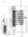
- Fig. 5 shows in block form oversampling clock recovery circuit 10 according to an embodiment of the present invention.
- oversampling clock recovery circuit 10 has eight phase comparators PD2 for sampling inputted data with 16-phase clocks CLK1 through CLK16 that are out of phase with each other for phase comparison, and controls the phase of clocks CLK1 through CLK16 based on phase difference information (UP, DOWN signals) that is outputted from phase comparators PD2.
- phase difference information UP, DOWN signals
- Oversampling clock recovery circuit 10 does not directly control the phase of clocks CLK1 through CLK16, but is supplied with two-phase clocks CLKa, CLKb fewer than 16-phase clocks CLK1 through CLK16 and controls the phase of two-phase clocks CLKa, CLKb with phase control circuit 11.
- Two-phase clocks CLKa, CLKb each have a frequency of 312.5 MHz and serve as a differential pair out of phase with each other by 1600 ps corresponding to one-half of the period.
- Delay-locked loop (DLL) 12 generates 16-phase clocks CLK1 through CLK16 from differential clocks outputted from phase control circuit 11, and supplies generated 16-phase clocks CLK1 through CLK16 to phase comparators PD2.
- Control voltage V2 is generated by a phase control signal based on the phase difference information (UP, DOWN signals) that is outputted from phase comparators PD2, and applied via a feedback loop to phase control circuit 11.
- Phase control circuit 11 uses control voltage V2 for controlling the phase of differential clocks CLKa, CLKb.
- differential clocks CLKa, CLKb are generated and supplied by phase-locked loop (PLL) 20.
- Phase-locked loop 20 comprises voltage-controlled oscillator 21, frequency multiplier DIV1 connected to voltage-controlled oscillator 21, phase comparator PD3, charge pump CP3, and low-pass filter LPF3.
- Voltage-controlled oscillator 21 includes voltage-controlled delay line 22 comprising a cascaded array of four differential buffers A1 through A4.
- phase comparator PD3 receives a clock whose frequency has been multiplied by frequency multiplier DIV1 and reference clock ref.CLK, compares the received clocks for phase, and outputs an UP/DOWN signal to charge pump CP3.
- Charge pump CP3 and low-pass filter LPF3 generate control voltage V3, which is applied via a feedback loop to differential buffers A1 through A4 to enable voltage-controlled oscillator 21 to generate a clock having a frequency of 312.5 MHz and a period of 3200 ps.
- Differential clocks CLKa, CLKb are extracted from voltage-controlled oscillator 21 and supplied to phase control circuit 11 in oversampling clock recovery circuit 10. Since phase-locked loop 20 is used, the clock having a stable frequency can be supplied to phase control circuit 11.
- Phase control circuit 11 may be of a digital control type or an analog control type.
- phase control circuit 11 is basically illustrated as a phase control circuit of the analog control type, and occasionally illustrated as a phase control circuit of the digital control type when necessary.
- Phase control circuit 11 is supplied with differential clocks CLKa, CLKb and also supplied with control voltage V2 from signal processor 13. Based on control voltage V2, phase control circuit 11 controls, e.g., advances or delays, the phase of differential clocks CLKa, CLKb.
- Differential clocks hereinafter referred to as “differential clocks CLKc, CLKd" which have been controlled in phase by phase control circuit 11 are outputted to delay-locked loop 12.
- Delay-locked loop 12 comprises voltage-controlled delay line 14 in the form of a cascaded array of eight differential buffers B1 through B8, phase comparator PD1 connected to voltage-controlled delay line 14, charge pump CP1, and low-pass filter LPF1.
- Differential clocks CLKc, CLKd are applied to first-stage differential buffer B1 and phase comparator PD1.
- Eighth-stage differential buffer B8 outputs differential clocks (hereinafter referred to as "differential clocks CLKe, CLKf" which are assumed to result from respective differential clocks CLKc, CLKd) having an overall delay caused by all buffers B1 through B8 after having passed through voltage-controlled delay line 14.
- Differential clocks CLKe, CLKf are applied to phase comparator PD1.
- Phase comparator PD1 compares clocks CLKc, CLKf and clocks CLKd, CLKe for phase to detect a phase error.
- phase comparator PD1 If the phase of clock CLKf (CLKe) lags the phase of clock CLKc (CLKd), then phase comparator PD1 outputs an UP signal to charge pump CP1. If the phase of clock CLKf (CLKe) leads the phase of clock CLKc (CLKd), then phase comparator PD1 outputs a DOWN signal to charge pump CP1.
- Charge pump CP1 and low-pass filter LPF1 generate control voltage V1 based on the phase difference information from phase comparator PD1, and applies generated control voltage V1 to differential buffers B1 through B8.
- voltage-controlled delay line 14 has a total delay time of 1600 ps which corresponds to one-half of the period of the clock whose frequency is 312.5 MHz. If the buffers of the delay line have identical characteristics and are supplied with identical control voltages, then the propagation delay time of each of the buffers has a value that is produced by dividing the total delay time of the delay line by the number of buffers of the delay line.
- differential buffers B1 through B8 of voltage-controlled delay line 14 have identical characteristics and are supplied with the same control voltage V1
- the propagation delay time of each of differential buffers B1 through B8 is 200 ps which is produced by diving the total delay time of 1600 ps by the number of those buffers, i.e., 8.
- the delay time of voltage-controlled delay line 14 is controlled so as to be constant by a feedback control process carried out by delay-locked loop 12.
- Eight differential buffers B1 through B8 of voltage-controlled delay line 14 output respective eight pairs of differential clocks that are out of phase by 200 ps. These outputted differential clocks are converted by converters CV1 from differential signals into single-phase signals and also from small amplitudes to large amplitudes, and then outputted to phase comparators PD2.
- delay-locked loop 12 serves to generate multiphase clocks CLK1 through CLK16, and signal processor 13 receives generated multiphase clocks CLK1 through CLK16.
- Delay-locked loop 12 generates multiphase clocks CLK1 through CLK16 that are kept out of phase highly accurately, which are supplied to signal processor 13.
- Signal processor 13 uses the supplied multiphase clocks to extract clocks for an oversampling process.
- Each of eight phase comparators PD2 of signal processor 13 compares successive three-phase clocks, which are 200 ps out of phase with each other, of the 16-phase clocks, with inputted serial data of 2.5 Gbps for phase. If the clocks lag the inputted data, then each of phase comparators PD2 outputs an UP signal. If the clocks lead the inputted data, then each of phase comparators PD2 outputs a DOWN signal.
- phase control circuit 11 Based on the UP or DOWN signal (phase difference information), signal processor 13 generates control voltage V2 and supplies generated control voltage V2 to phase control circuit 11, which is of the analog control type, in order to synchronize the clocks with the inputted data in phase.
- phase control circuit 11 controls, e.g., advances or delays, the phase of differential clocks CLKa, CLKb according to control voltage V2.
- Differential clocks CLKc, CLKd which have been controlled in phase by phase control circuit 11 are outputted to delay-locked loop 12.
- Oversampling clock recovery circuit 10 repeats the above operation to keep 16-phase clocks CLK1 through CLK16 supplied to signal processor 13 accurately out of phase and synchronize 16-phase clocks CLK1 through CLK16 with the inputted data.
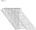
- FIG. 8 shows the waveforms of the data and the clocks that are held in synchronism with each other. Even if the clocks lag the data as shown in Fig. 1B, when oversampling clock recovery circuit 10 operates in the manner described above, even-numbered clocks CLK2, CLK4, ⁇ are held in synchronism with edges of the data bits, whereas odd-numbered clocks CLK1, CLK3, ⁇ are held in synchronism with centers of the data bits, as shown in Fig. 8.
- Oversampling clock recovery circuit 10 is capable of allowing 16-phase clocks CLK1 through CLK16 to follow the data as they fluctuate in phase in order to cause odd-numbered clocks CLK1, CLK3, ⁇ to sample the inputted data in their reliably open regions, i.e., regions where the values of the inputted data are stably determined.
- signal processor 13 can be performed by any of various conventional arrangements. One arrangement of signal processor 13 will be described below.
- a specific arrangement of signal processor 13 for generating control voltage V4 based on the UP/DOWN signal outputted from phase comparators PD2 comprises signal processing circuit 15, charge pump CP2, and low-pass filter LPF2.
- Signal processing circuit 15 comprises a majority circuit and an averaging circuit.
- Each of eight phase comparators PD2 uses successive three-phase clocks, which are 200 ps out of phase with each other, of the 16-phase clocks, and compares the inputted data with the multiphase clocks. For example, eight sets of three clocks CLK1, CLK2, CLK3, three clocks CLK3, CLK4, CLK5, three clocks CLK5, CLK6, CLK7, three clocks CLK7, CLK8, CLK9, three clocks CLK9, CLK10, CLK11, three clocks CLK11, CLK12, CLK13, three clocks CLK13, CLK14, CLK15, and three clocks CLK15, CLK16, CLK1 are used by respective eight phase comparators PD2.
- differential buffers B1 through B8 thereof output differential clocks CLK1, CLK9, differential clocks CLK2, CLK10, differential clocks CLK3, CLK11, differential clocks CLK4, CLK12, differential clocks CLK5, CLK13, differential clocks LCK6, CLK14, differential clocks CLK7, CLK15, differential clocks CLK8, CLK16, respectively.
- the interconnections of oversampling clock recovery circuit are arranged as shown in Fig.
- Phase comparators PD2 that are supplied with the respective sets of successive three clocks compare the clocks with the inputted data. If the clocks lag the inputted data, then phase comparators PD2 output an UP signal to signal processing circuit 15. If the clocks lead the inputted data, then phase comparators PD2 output a DOWN signal to signal processing circuit 15. Each time signal processing circuit 15 receives UP/DOWN signals from phase comparators PD2, the majority circuit in signal processing circuit 5 determines a majority of output signals from phase comparators PD2, and determines the phase difference between the data and the clocks at that moment.
- the averaging circuit in signal processing circuit 5 averages several UP/DOWN signals that have been determined as a majority.
- the averaged UP/DOWN signal is outputted to charge pump CP2, charging or discharging charge pump CP2.
- charge pump CP2 charging or discharging charge pump CP2.
- the averaging circuit in signal processing circuit 5 serves as a filter for blocking high-frequency components and passing low-frequency components.
- phase control circuit 11 Charges charged in and discharged from charge pump CP2 are passed through low-pass filter LPF2, which produces analog control voltage V2 and output analog control voltage V2 to phase control circuit 11 of the analog control type. If phase control circuit 11 is of the digital control type, then a phase control signal is outputted directly to phase control circuit 11 without passing through low-pass filter LPF2.
- signal processor 13 has been described above by way of illustrative example only, and may be carried out by any of various other circuit arrangement.
- Oversampling clock recovery circuit 10 according to the above embodiment as it is applied to a transceiver having a number of serial input/output channels will be described below with reference to Fig. 6.
- oversampling clock recovery circuits 10 are provided in respective channels ch1 through ch(n).
- Single phase-locked loop 20 generates differential clocks and distribute the generated differential clocks to oversampling clock recovery circuits 10(1) through 10(n).
- the oversampling clock recovery circuit 10 in each channel operates in the manner described above, it can produce multiphase clocks having the same frequency as the distributed differential clocks.
- the oversampling clock recovery circuit that is used in a multichannel application offers the following advantages:
- oversampling clock recovery circuit 10 is provided in each channel, no voltage-controlled oscillator is included in each channel, and hence there is no possibility of undue interference such as clock resonance between the channels.
- oversampling clock recovery circuit 10 is provided in each channel, it is not necessary to distribute multiphase clocks to each channel, but a relatively small number of clocks may be distributed to each channel. Therefore, no unduly large increase in the consumption of electric power is needed for the distribution of multiphase clocks.
- oversampling clock recovery circuit 10 is provided in each channel, it is not necessary to distribute multiphase clocks to each channel, but a relatively small number of clocks may be distributed to each channel. Therefore, the system is free of a reduction in the quality of multiphase clocks when the clocks are distributed, due to variations or skews of phase intervals between the multiphase clocks.
- the fifth advantage is that since the phase is controlled with respect to a relatively small number of clocks. Therefore, the circuit scale and the power consumption can be made smaller than the conventional arrangement (conventional clock recovery circuit 60) which controls the phase of multiphase clocks.
- the sixth advantage is that because a relatively small number of clocks which have been controlled highly accurately in phase by phase control circuit 11 are developed into multiphase clocks by the delay-locked loop immediately prior to phase comparison, it is possible to supply phase comparators PD2 with extremely high-quality multiphase clocks that are kept out of phase accurately.
- the recovery process is made much more reliable than the conventional arrangement (conventional clock recovery circuit 60) which comprises a plurality of parallel phase control circuits.
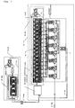
- Oversampling clock recovery circuit 30 according to another embodiment of the present invention will be described below with reference to Fig. 7.
- oversampling clock recovery circuit 30 is similar to oversampling clock recovery circuit 10 in that it receives a clock from phase-locked loop 20, but differs therefrom in that it receives a single-phase click CLKg.
- oversampling clock recovery circuit 30 is similar to oversampling clock recovery circuit 10 in that it has signal processor 13, but differs therefrom in that it has phase control circuit 31 and delay-locked loop 32 which are of a single-phase arrangement.
- Delay-locked loop 32 comprises voltage-controlled delay line 34 in the form of a cascaded array of 16 single-phase buffers C1 through C16, phase comparator PD4 connected to voltage-controlled delay line 34, charge pump CP4, and low-pass filter LPF4.
- Differential clocks produced by delay-locked loop 20 are converted by converter CV2 from differential signals into a single-phase signal and also from a small amplitude into a large amplitude. As a result, converter CV2 outputs single-phase clock CLKg, which is inputted to phase control circuit 31.
- clock CLKg is controlled in phase by phase control circuit 31.
- the clock (hereinafter referred to as “clock CLKh") which has been controlled in phase by phase control circuit 31 is applied to first-stage differential buffer C1 and phase comparator PD4.
- 16th-stage differential buffer C16 outputs a clock (hereinafter referred to as "clock CLKi") having an overall delay caused by all buffers C1 through C16 after having passed through voltage-controlled delay line 34.
- Clock CLKi is applied to phase comparator PD4.
- Phase comparator PD4 compares clocks CLKh, CLKi for phase to detect a phase error. If the phase of clock CLKi lags the phase of clock CLKh, then phase comparator PD4 outputs an UP signal to charge pump CP4. If the phase of clock CLKi leads the phase of clock CLKh, then phase comparator PD4 outputs a DOWN signal to charge pump CP4.
- Charge pump CP4 and low-pass filter LPF4 generate control voltage V1 based on the phase difference information from phase comparator PD4, and applies generated control voltage V1 to buffers C1 through C16.
- voltage-controlled delay line 34 has a total delay time of 3200 ps which corresponds to one period of the clock whose frequency is 312.5 MHz. If the buffers of the delay line have identical characteristics and are supplied with identical control voltages, then the propagation delay time of each of the buffers has a value that is produced by dividing the total delay time of the delay line by the number of buffers of the delay line.
- buffers C1 through C16 of voltage-controlled delay line 34 have identical characteristics and are supplied with the same control voltage V1
- the propagation delay time of each of buffers C1 through C16 is 200 ps which is produced by diving the total delay time of 3200 ps by the number of those buffers, i.e., 16.
- the delay time of voltage-controlled delay line 34 is controlled so as to be constant by a feedback control process carried out by delay-locked loop 32.
- 16 buffers C1 through C16 of voltage-controlled delay line 34 output respective 16 clocks that are out of phase by 200 ps. Sets of successive three clocks are outputted respectively to phase comparators PD2.
- 16-phase clocks that are successively out of phase by 200 ps are denoted by CLK1, CLK2, CLK3, ⁇ , CLK16. Since delay-locked loop 32 shown in Fig. 7 use inverters as buffers C1 through C16, buffers C1 through C16 output clocks CLK1, CLK10, CLK3, CLK12, CLK5, CLK14, CLK7, CLK16, CLK9, CLK2, CLK11, CLk4, CLK13, CLK6, CLK15, CLK8, respectively.
- the interconnections of oversampling clock recovery circuit are arranged as shown in Fig.
- phase comparators PD2 sets of successive three clocks CLK1, CLK2, CLK3, successive three clocks CLK3, CLK4, CLK5, successive three clocks CLK5, CLK6, CLK7, successive three clocks CLK7, CLK8, CLK9, successive three clocks CLK9, CLK10, CLK11, successive three clocks CLK11, CLK12, CLK13, successive three clocks CLK13, CLK14, CLK15, and successive three clocks CLK15, CLK16, CLK1 are inputted respectively to phase comparators PD2 in the order from the left.
- oversampling clock recovery circuit 30 After the sets of successive three clocks are inputted to phase comparators PD2, oversampling clock recovery circuit 30 repeatedly operates in the same manner as oversampling clock recovery circuit 10 to keep 16-phase clocks CLK1 through CLK16 supplied to signal processor 13 out of phase accurately and synchronize 16-phase clocks CLK1 through CLK16 with the inputted data in phase.
- oversampling clock recovery circuit 30 Since oversampling clock recovery circuit 30 according to the present embodiment has phase control circuit 31 and delay-locked loop 32 which are of a single-phase arrangement, it can use large-amplitude CMOS logic components, and hence has a lower power requirement than oversampling clock recovery circuits 10, 40, 60.
- Conventional oversampling clock recovery circuit 40 with a voltage-controlled oscillator tends to have its jitter characteristics degraded if voltage-controlled oscillator 41 is of a single-phase arrangement.
- phase control circuit 31 and delay-locked loop 32 are of a single-phase arrangement. Therefore, oversampling clock recovery circuit 30 according to the present embodiment is free of the above tendency of conventional oversampling clock recovery circuit 40. Consequently, oversampling clock recovery circuit 30 has a low power requirement though its jitter characteristics remain in a desired good level.
- oversampling clock recovery circuit 30 As with oversampling clock recovery circuit 10, oversampling clock recovery circuit 30 according to the present embodiment is well applicable to a transceiver having a number of serial input/output channels, and offers the same advantages.
- an oversampling clock recovery circuit does not use a voltage-controlled oscillator, but has a phase control circuit and an analog delay-locked loop.
- the oversampling clock recovery circuit is supplied with a relatively small number of clocks from a phase control circuit, controls the phase of the relatively small number of clocks, develops the phase-controlled clocks into a number of clocks in as many phases as required for phase comparison, and supplies the clocks to phase comparators.
- the oversampling clock recovery circuit has its jitter characteristics improved and is capable of generating high-quality clocks.
- the oversampling clock recovery circuit is applied to a transceiver having a number of serial input/output channels, then it can produce high-quality clocks as it is free any possibility of undue interference such as clock resonance between the channels.
- the oversampling clock recovery circuit is applied to multiple channels, then it has a high circuit area efficiency, a high electric power efficiency, and a high clock distribution efficiency.
Landscapes
- Engineering & Computer Science (AREA)
- Computer Networks & Wireless Communication (AREA)
- Signal Processing (AREA)
- Stabilization Of Oscillater, Synchronisation, Frequency Synthesizers (AREA)
- Synchronisation In Digital Transmission Systems (AREA)
- Dc Digital Transmission (AREA)
Abstract
Description
Claims (3)
- An oversampling clock recovery circuit having a plurality of phase comparators for sampling inputted data with a number of clocks which are out of phase with each other for phase comparison, for controlling the phase of the clocks based on phase difference information output from the phase comparators, comprising:a phase control circuit for being supplied with fewer clocks than said number of clocks and controlling the phase of the supplied clocks; anda delay-locked loop for generating said number of clocks based on said fewer clocks controlled in phase by said phase control circuit, and supplying the generated number of clocks to said phase comparators;the arrangement being such that a phase control signal based on the phase difference information output from the phase comparators is supplied via a feedback loop to said phase control circuit.
- The oversampling clock recovery circuit according to claim 1, wherein said fewer clocks comprise one or two clocks.
- The oversampling clock recovery circuit according to claim 1, wherein said fewer clocks comprise one clock.
Applications Claiming Priority (2)
| Application Number | Priority Date | Filing Date | Title |
|---|---|---|---|
| JP2000139089 | 2000-05-11 | ||
| JP2000139089A JP4425426B2 (en) | 2000-05-11 | 2000-05-11 | Oversampling clock recovery circuit |
Publications (3)
| Publication Number | Publication Date |
|---|---|
| EP1154595A2 true EP1154595A2 (en) | 2001-11-14 |
| EP1154595A3 EP1154595A3 (en) | 2004-06-30 |
| EP1154595B1 EP1154595B1 (en) | 2006-12-27 |
Family
ID=18646599
Family Applications (1)
| Application Number | Title | Priority Date | Filing Date |
|---|---|---|---|
| EP01111006A Expired - Lifetime EP1154595B1 (en) | 2000-05-11 | 2001-05-07 | Oversampling clock recovery circuit |
Country Status (5)
| Country | Link |
|---|---|
| US (1) | US6456128B1 (en) |
| EP (1) | EP1154595B1 (en) |
| JP (1) | JP4425426B2 (en) |
| KR (1) | KR100380771B1 (en) |
| DE (1) | DE60125455T2 (en) |
Cited By (2)
| Publication number | Priority date | Publication date | Assignee | Title |
|---|---|---|---|---|
| WO2003077466A1 (en) * | 2002-02-21 | 2003-09-18 | Infineon Technologies Ag | Device for recovering data from a received data signal |
| WO2004002052A1 (en) * | 2002-06-25 | 2003-12-31 | Bogdan John W | Digital signal processing of multi-sampled phase |
Families Citing this family (28)
| Publication number | Priority date | Publication date | Assignee | Title |
|---|---|---|---|---|
| US6791380B2 (en) * | 2001-11-27 | 2004-09-14 | Winbond Electronics Corporation | Universal clock generator |
| DE10206370B4 (en) * | 2002-02-15 | 2005-08-25 | Infineon Technologies Ag | Method and device for phase detection |
| JP3660638B2 (en) * | 2002-03-27 | 2005-06-15 | 株式会社東芝 | Clock extraction circuit |
| US6774689B1 (en) | 2002-05-23 | 2004-08-10 | Cypress Semiconductor Corp. | Triple input phase detector and methodology for setting delay between two sets of phase outputs |
| US6657466B1 (en) * | 2002-05-23 | 2003-12-02 | Cypress Semiconductor Corp. | System and method for generating interleaved multi-phase outputs from a nested pair of phase locked loops |
| CN100358238C (en) * | 2002-09-02 | 2007-12-26 | 瑞昱半导体股份有限公司 | Data recovery system and method thereof |
| JP4158465B2 (en) | 2002-09-10 | 2008-10-01 | 日本電気株式会社 | CLOCK REPRODUCTION DEVICE AND ELECTRONIC DEVICE USING CLOCK REPRODUCTION DEVICE |
| JP3883063B2 (en) | 2002-10-31 | 2007-02-21 | ローム株式会社 | Clock generator |
| KR100531457B1 (en) * | 2003-07-23 | 2005-11-28 | (주)다윈텍 | Delay Locked Loop For Generating Multi-Phase Clocks Without Voltage-Controlled Oscillator |
| US7668271B2 (en) * | 2003-09-30 | 2010-02-23 | Rambus Inc. | Clock-data recovery (“CDR”) circuit, apparatus and method for variable frequency data |
| US7486752B1 (en) * | 2003-12-17 | 2009-02-03 | Altera Corporation | Alignment of clock signal with data signal |
| US7696797B1 (en) * | 2005-03-31 | 2010-04-13 | Schnaitter William N | Signal generator with output frequency greater than the oscillator frequency |
| DE102005023427B3 (en) * | 2005-05-20 | 2006-10-12 | Infineon Technologies Ag | Delay control loop for digital circuits has control unit that switches delay cells in delay circuit to adjust delay time of delay circuit |
| US7532038B2 (en) * | 2005-07-01 | 2009-05-12 | Via Technologies, Inc. | Phase detecting circuit having adjustable gain curve and method thereof |
| JP4668750B2 (en) | 2005-09-16 | 2011-04-13 | 富士通株式会社 | Data recovery circuit |
| US8520776B2 (en) * | 2006-01-19 | 2013-08-27 | Judith Ann Rea | Data recovery system for source synchronous data channels |
| US7809085B2 (en) * | 2006-01-19 | 2010-10-05 | Redmere Technology Ltd. | Data recovery system for source synchronous data channels |
| KR100834393B1 (en) | 2006-10-31 | 2008-06-04 | 주식회사 하이닉스반도체 | Clock data recovery device. |
| US7924885B2 (en) * | 2006-11-20 | 2011-04-12 | Siverge Networks Ltd | Methods and apparatuses for circuit emulation multi-channel clock recovery |
| JP4825710B2 (en) * | 2007-03-16 | 2011-11-30 | 株式会社リコー | Multiphase clock generation circuit and serial data reception circuit |
| US8179162B2 (en) * | 2010-07-13 | 2012-05-15 | Taiwan Semiconductor Manufacturing Company, Ltd. | Phase-lock assistant circuitry |
| US8588358B2 (en) | 2011-03-11 | 2013-11-19 | Taiwan Semiconductor Manufacturing Company, Ltd. | Clock and data recovery using LC voltage controlled oscillator and delay locked loop |
| US8797075B2 (en) * | 2012-06-25 | 2014-08-05 | Intel Corporation | Low power oversampling with reduced-architecture delay locked loop |
| US8779815B2 (en) * | 2012-06-25 | 2014-07-15 | Intel Corporation | Low power oversampling with delay locked loop implementation |
| KR102298160B1 (en) * | 2015-08-13 | 2021-09-03 | 삼성전자주식회사 | Semiconductor device and the communication system including thereof |
| US11616501B2 (en) * | 2017-10-28 | 2023-03-28 | Solos Technology Limited | Programmable fractional time delay in digitally oversampled microphone systems, circuits, and methods |
| CN116055927B (en) * | 2023-04-03 | 2023-06-02 | 深圳市紫光同创电子有限公司 | Data double oversampling method, system, equipment and storage medium |
| CN117667815B (en) * | 2023-12-01 | 2024-10-18 | 广东高云半导体科技股份有限公司 | Deskewing circuit, deskewing method, computer storage medium and terminal |
Family Cites Families (13)
| Publication number | Priority date | Publication date | Assignee | Title |
|---|---|---|---|---|
| JPH0583240A (en) * | 1991-09-19 | 1993-04-02 | Fujitsu Ltd | Clock recovery circuit |
| JPH0621808A (en) * | 1992-07-01 | 1994-01-28 | Hitachi Ltd | Clock recovery circuit |
| JPH06152668A (en) * | 1992-11-10 | 1994-05-31 | Matsushita Electric Ind Co Ltd | Clock recovery circuit |
| JPH07302938A (en) * | 1994-04-28 | 1995-11-14 | Sony Corp | Piezoelectric ceramic transformer and manufacturing method thereof |
| EP0758171A3 (en) * | 1995-08-09 | 1997-11-26 | Symbios Logic Inc. | Data sampling and recovery |
| US5694062A (en) | 1996-02-02 | 1997-12-02 | Lsi Logic Corporation | Self-timed phase detector and method |
| JPH09275396A (en) * | 1996-04-04 | 1997-10-21 | Nec Eng Ltd | Clock recovery circuit |
| US6026134A (en) * | 1997-06-19 | 2000-02-15 | Cypress Semiconductor Corp. | Phase locked loop (PLL) with linear parallel sampling phase detector |
| US5963606A (en) * | 1997-06-27 | 1999-10-05 | Sun Microsystems, Inc. | Phase error cancellation method and apparatus for high performance data recovery |
| JP3109588B2 (en) * | 1998-03-12 | 2000-11-20 | 日本電気株式会社 | Oversampling type clock recovery circuit |
| JP3109587B2 (en) * | 1998-03-12 | 2000-11-20 | 日本電気株式会社 | Oversampling type clock recovery circuit |
| JP3077661B2 (en) * | 1998-03-12 | 2000-08-14 | 日本電気株式会社 | Oversampling type clock recovery circuit |
| GB2336074B (en) * | 1998-03-30 | 2002-12-04 | 3Com Technologies Ltd | Method and apparatus for the phase alignment of data in high-speed parallel data buses using a multi-phase low frequency sampling clock |
-
2000
- 2000-05-11 JP JP2000139089A patent/JP4425426B2/en not_active Expired - Fee Related
-
2001
- 2001-05-03 US US09/847,311 patent/US6456128B1/en not_active Expired - Fee Related
- 2001-05-07 EP EP01111006A patent/EP1154595B1/en not_active Expired - Lifetime
- 2001-05-07 DE DE60125455T patent/DE60125455T2/en not_active Expired - Lifetime
- 2001-05-10 KR KR10-2001-0025400A patent/KR100380771B1/en not_active Expired - Fee Related
Cited By (4)
| Publication number | Priority date | Publication date | Assignee | Title |
|---|---|---|---|---|
| WO2003077466A1 (en) * | 2002-02-21 | 2003-09-18 | Infineon Technologies Ag | Device for recovering data from a received data signal |
| CN100338903C (en) * | 2002-02-21 | 2007-09-19 | 因芬尼昂技术股份公司 | Device for recovering data from a received data signal |
| WO2004002052A1 (en) * | 2002-06-25 | 2003-12-31 | Bogdan John W | Digital signal processing of multi-sampled phase |
| US7564934B2 (en) * | 2002-06-25 | 2009-07-21 | John W. Bogdan | Digital signal processing of multi-sampled phase |
Also Published As
| Publication number | Publication date |
|---|---|
| US6456128B1 (en) | 2002-09-24 |
| KR20010104240A (en) | 2001-11-24 |
| JP4425426B2 (en) | 2010-03-03 |
| EP1154595B1 (en) | 2006-12-27 |
| DE60125455D1 (en) | 2007-02-08 |
| JP2001320353A (en) | 2001-11-16 |
| EP1154595A3 (en) | 2004-06-30 |
| US20020030522A1 (en) | 2002-03-14 |
| DE60125455T2 (en) | 2007-10-11 |
| KR100380771B1 (en) | 2003-04-18 |
Similar Documents
| Publication | Publication Date | Title |
|---|---|---|
| EP1154595B1 (en) | Oversampling clock recovery circuit | |
| KR0185474B1 (en) | Clock recovery circuit and elements using this clock recovery circuit | |
| US6166572A (en) | Voltage-controlled delay line, direct phase controlled voltage-controlled oscillator, clock/data recovery circuit, and clock/data recovery apparatus | |
| KR100644127B1 (en) | Dual loop DL based on voltage controlled delay line with infinite phase shift | |
| US8170168B2 (en) | Clock data recovery circuit | |
| JP4029568B2 (en) | Clock generation circuit, serial / parallel converter, parallel / serial converter, and semiconductor device | |
| CN101145898A (en) | Clock and data recovery circuit and method for recovering clock and data | |
| KR100195855B1 (en) | Clock synchronization scheme for fractional multiplication systems | |
| US20080174347A1 (en) | Clock synchronization system and semiconductor integrated circuit | |
| US6917232B2 (en) | Method and apparatus for generating a quadrature clock | |
| US20070223638A1 (en) | Isophase Multiphase Clock Signal Generation Circuit and Serial Digital Data Receiving Circuit Using the Same | |
| US7254205B2 (en) | Signal processing method and apparatus for ensuring a desired relationship between signals | |
| US6104326A (en) | Bit synchronization apparatus for recovering high speed NRZ data | |
| JP2021179798A (en) | Timing synchronization circuit | |
| US9582028B1 (en) | Circuits and methods of TAF-DPS based chip level global clock signal distribution | |
| US6967536B2 (en) | Phase-locked loop circuit reducing steady state phase error | |
| US6477657B1 (en) | Circuit for I/O clock generation | |
| US7081783B2 (en) | Method and apparatus for generating and controlling a multiphase clock | |
| KR100293256B1 (en) | A fast lock on time mixed mode delay locked loop with low jitter | |
| KR100917539B1 (en) | Method and apparatus for generating and synchronizing multiple clocks | |
| US7471752B2 (en) | Data transmission synchronization | |
| CN101414820B (en) | Digital frequency synthesis and synchronous circuit | |
| US7653169B2 (en) | Timing adjustment for data transmitting/receiving circuit | |
| KR100418017B1 (en) | Data and clock recovery circuit | |
| KR100889337B1 (en) | Clock data recovery circuit |
Legal Events
| Date | Code | Title | Description |
|---|---|---|---|
| PUAI | Public reference made under article 153(3) epc to a published international application that has entered the european phase |
Free format text: ORIGINAL CODE: 0009012 |
|
| AK | Designated contracting states |
Kind code of ref document: A2 Designated state(s): AT BE CH CY DE DK ES FI FR GB GR IE IT LI LU MC NL PT SE TR |
|
| AX | Request for extension of the european patent |
Free format text: AL;LT;LV;MK;RO;SI |
|
| RAP1 | Party data changed (applicant data changed or rights of an application transferred) |
Owner name: NEC ELECTRONICS CORPORATION |
|
| PUAL | Search report despatched |
Free format text: ORIGINAL CODE: 0009013 |
|
| AK | Designated contracting states |
Kind code of ref document: A3 Designated state(s): AT BE CH CY DE DK ES FI FR GB GR IE IT LI LU MC NL PT SE TR |
|
| AX | Request for extension of the european patent |
Extension state: AL LT LV MK RO SI |
|
| RIC1 | Information provided on ipc code assigned before grant |
Ipc: 7H 03L 7/08 B Ipc: 7H 04L 7/033 A Ipc: 7H 04L 25/14 B |
|
| 17P | Request for examination filed |
Effective date: 20040601 |
|
| 17Q | First examination report despatched |
Effective date: 20040804 |
|
| AKX | Designation fees paid |
Designated state(s): DE GB |
|
| GRAP | Despatch of communication of intention to grant a patent |
Free format text: ORIGINAL CODE: EPIDOSNIGR1 |
|
| GRAS | Grant fee paid |
Free format text: ORIGINAL CODE: EPIDOSNIGR3 |
|
| GRAA | (expected) grant |
Free format text: ORIGINAL CODE: 0009210 |
|
| AK | Designated contracting states |
Kind code of ref document: B1 Designated state(s): DE GB |
|
| REG | Reference to a national code |
Ref country code: GB Ref legal event code: FG4D |
|
| REF | Corresponds to: |
Ref document number: 60125455 Country of ref document: DE Date of ref document: 20070208 Kind code of ref document: P |
|
| PLBE | No opposition filed within time limit |
Free format text: ORIGINAL CODE: 0009261 |
|
| STAA | Information on the status of an ep patent application or granted ep patent |
Free format text: STATUS: NO OPPOSITION FILED WITHIN TIME LIMIT |
|
| 26N | No opposition filed |
Effective date: 20070928 |
|
| REG | Reference to a national code |
Ref country code: DE Ref legal event code: R082 Ref document number: 60125455 Country of ref document: DE Representative=s name: SAMSON & PARTNER, PATENTANWAELTE, DE |
|
| REG | Reference to a national code |
Ref country code: DE Ref legal event code: R082 Ref document number: 60125455 Country of ref document: DE Representative=s name: SAMSON & PARTNER, PATENTANWAELTE, DE Effective date: 20120828 Ref country code: DE Ref legal event code: R081 Ref document number: 60125455 Country of ref document: DE Owner name: RENESAS ELECTRONICS CORPORATION, JP Free format text: FORMER OWNER: NEC ELECTRONICS CORP., KAWASAKI, JP Effective date: 20120828 Ref country code: DE Ref legal event code: R081 Ref document number: 60125455 Country of ref document: DE Owner name: RENESAS ELECTRONICS CORPORATION, KAWASAKI-SHI, JP Free format text: FORMER OWNER: NEC ELECTRONICS CORP., KAWASAKI, KANAGAWA, JP Effective date: 20120828 |
|
| PGFP | Annual fee paid to national office [announced via postgrant information from national office to epo] |
Ref country code: DE Payment date: 20130515 Year of fee payment: 13 Ref country code: GB Payment date: 20130501 Year of fee payment: 13 |
|
| REG | Reference to a national code |
Ref country code: DE Ref legal event code: R119 Ref document number: 60125455 Country of ref document: DE |
|
| GBPC | Gb: european patent ceased through non-payment of renewal fee |
Effective date: 20140507 |
|
| REG | Reference to a national code |
Ref country code: DE Ref legal event code: R119 Ref document number: 60125455 Country of ref document: DE Effective date: 20141202 |
|
| PG25 | Lapsed in a contracting state [announced via postgrant information from national office to epo] |
Ref country code: DE Free format text: LAPSE BECAUSE OF NON-PAYMENT OF DUE FEES Effective date: 20141202 |
|
| PG25 | Lapsed in a contracting state [announced via postgrant information from national office to epo] |
Ref country code: GB Free format text: LAPSE BECAUSE OF NON-PAYMENT OF DUE FEES Effective date: 20140507 |