EP1154533A1 - Light source containing a distributed feedback laser and an integrated optical modulator - Google Patents
Light source containing a distributed feedback laser and an integrated optical modulator Download PDFInfo
- Publication number
- EP1154533A1 EP1154533A1 EP01111372A EP01111372A EP1154533A1 EP 1154533 A1 EP1154533 A1 EP 1154533A1 EP 01111372 A EP01111372 A EP 01111372A EP 01111372 A EP01111372 A EP 01111372A EP 1154533 A1 EP1154533 A1 EP 1154533A1
- Authority
- EP
- European Patent Office
- Prior art keywords
- modulator
- semiconductor laser
- diffraction grating
- dfb
- substrate
- Prior art date
- Legal status (The legal status is an assumption and is not a legal conclusion. Google has not performed a legal analysis and makes no representation as to the accuracy of the status listed.)
- Withdrawn
Links
- 230000003287 optical effect Effects 0.000 title claims abstract description 29
- 239000004065 semiconductor Substances 0.000 claims abstract description 34
- 239000000758 substrate Substances 0.000 claims abstract description 22
- 230000010363 phase shift Effects 0.000 claims abstract description 7
- 230000005540 biological transmission Effects 0.000 description 12
- 239000012071 phase Substances 0.000 description 11
- 238000000034 method Methods 0.000 description 5
- 230000008859 change Effects 0.000 description 3
- 238000004891 communication Methods 0.000 description 3
- 238000005259 measurement Methods 0.000 description 3
- 238000004088 simulation Methods 0.000 description 3
- 229910000530 Gallium indium arsenide Inorganic materials 0.000 description 2
- 238000005253 cladding Methods 0.000 description 2
- 230000007547 defect Effects 0.000 description 2
- 230000004075 alteration Effects 0.000 description 1
- 238000003486 chemical etching Methods 0.000 description 1
- 230000008878 coupling Effects 0.000 description 1
- 238000010168 coupling process Methods 0.000 description 1
- 238000005859 coupling reaction Methods 0.000 description 1
- 230000007423 decrease Effects 0.000 description 1
- 230000003247 decreasing effect Effects 0.000 description 1
- 238000010586 diagram Methods 0.000 description 1
- 238000010894 electron beam technology Methods 0.000 description 1
- 238000005530 etching Methods 0.000 description 1
- 230000001747 exhibiting effect Effects 0.000 description 1
- 239000002184 metal Substances 0.000 description 1
- 238000012986 modification Methods 0.000 description 1
- 230000004048 modification Effects 0.000 description 1
- 239000013307 optical fiber Substances 0.000 description 1
- 230000009467 reduction Effects 0.000 description 1
- 238000000927 vapour-phase epitaxy Methods 0.000 description 1
Images




Classifications
-
- H—ELECTRICITY
- H01—ELECTRIC ELEMENTS
- H01S—DEVICES USING THE PROCESS OF LIGHT AMPLIFICATION BY STIMULATED EMISSION OF RADIATION [LASER] TO AMPLIFY OR GENERATE LIGHT; DEVICES USING STIMULATED EMISSION OF ELECTROMAGNETIC RADIATION IN WAVE RANGES OTHER THAN OPTICAL
- H01S5/00—Semiconductor lasers
- H01S5/10—Construction or shape of the optical resonator, e.g. extended or external cavity, coupled cavities, bent-guide, varying width, thickness or composition of the active region
- H01S5/12—Construction or shape of the optical resonator, e.g. extended or external cavity, coupled cavities, bent-guide, varying width, thickness or composition of the active region the resonator having a periodic structure, e.g. in distributed feedback [DFB] lasers
- H01S5/124—Construction or shape of the optical resonator, e.g. extended or external cavity, coupled cavities, bent-guide, varying width, thickness or composition of the active region the resonator having a periodic structure, e.g. in distributed feedback [DFB] lasers incorporating phase shifts
-
- H—ELECTRICITY
- H01—ELECTRIC ELEMENTS
- H01S—DEVICES USING THE PROCESS OF LIGHT AMPLIFICATION BY STIMULATED EMISSION OF RADIATION [LASER] TO AMPLIFY OR GENERATE LIGHT; DEVICES USING STIMULATED EMISSION OF ELECTROMAGNETIC RADIATION IN WAVE RANGES OTHER THAN OPTICAL
- H01S5/00—Semiconductor lasers
- H01S5/02—Structural details or components not essential to laser action
- H01S5/026—Monolithically integrated components, e.g. waveguides, monitoring photo-detectors, drivers
- H01S5/0265—Intensity modulators
-
- H—ELECTRICITY
- H01—ELECTRIC ELEMENTS
- H01S—DEVICES USING THE PROCESS OF LIGHT AMPLIFICATION BY STIMULATED EMISSION OF RADIATION [LASER] TO AMPLIFY OR GENERATE LIGHT; DEVICES USING STIMULATED EMISSION OF ELECTROMAGNETIC RADIATION IN WAVE RANGES OTHER THAN OPTICAL
- H01S5/00—Semiconductor lasers
- H01S5/02—Structural details or components not essential to laser action
- H01S5/028—Coatings ; Treatment of the laser facets, e.g. etching, passivation layers or reflecting layers
- H01S5/0287—Facet reflectivity
-
- H—ELECTRICITY
- H01—ELECTRIC ELEMENTS
- H01S—DEVICES USING THE PROCESS OF LIGHT AMPLIFICATION BY STIMULATED EMISSION OF RADIATION [LASER] TO AMPLIFY OR GENERATE LIGHT; DEVICES USING STIMULATED EMISSION OF ELECTROMAGNETIC RADIATION IN WAVE RANGES OTHER THAN OPTICAL
- H01S5/00—Semiconductor lasers
- H01S5/10—Construction or shape of the optical resonator, e.g. extended or external cavity, coupled cavities, bent-guide, varying width, thickness or composition of the active region
- H01S5/1039—Details on the cavity length
Definitions
- the present invention relates to a light source integrated with a modulator and a module for optical communication, and especially to the structure for the light source integrated with the modulator and suitable for a light source for long distance trunk used in wavelength division multiplexing (WDM).
- WDM wavelength division multiplexing
- a module As a light source for long distance trunk used in WDM, a module is put into practice which includes a distributed feedback semiconductor laser (DFB-LD) and a field absorbing modulator (MOD) on a single semiconductor substrate.
- DFB-LD distributed feedback semiconductor laser
- MOD field absorbing modulator
- a resistance to distribution or an ability of transmitting long-distance signals in the DFB-LD is the most important parameter exhibiting element performance.
- the selection of products having no defect therein is currently conducted by measuring the resistance to distribution or the power penalty after the transmission of each element. It is an important subject to increase the yield of the selection for decreasing the cost of the light source.
- Murotani et al. reported the dependency of the single mode yield of the DFB/MOD module having an asymmetrical ⁇ /4 phase shifter (a structure obtained by moving the ⁇ /4 phase shift region of the diffraction grating from the central position of the DFB-LD, hereinafter referred to as "asymmetrical ⁇ /4-DFB/MOD") on a ⁇ L value of a diffraction grating in the DFB-LD in the Electronics Society Meeting (C-4-15, p242) held in September 1999 by the Institute of Electronics, Information and Communication Engineers.
- asymmetrical ⁇ /4-DFB/MOD a structure obtained by moving the ⁇ /4 phase shift region of the diffraction grating from the central position of the DFB-LD
- the single mode yield rapidly decreases with the increase of the ⁇ L in the asymmetrical ⁇ /4-DFB/MOD module.
- Conventional publications including the above publication describe neither the yield of the power source integrated with the modulator separately from the single mode yield, nor the optimum structure regarding determination of the facet reflection rate and of the ⁇ L.
- the optimum structure has not been conventionally established by considering the dependency of the diffraction grating on the ⁇ L value and the dependency of the modulator on the facet reflection rate.
- an object of the present invention is to increase the yield of obtaining DFB/MOD module having no defect by considering the dependency of the ⁇ L value of the diffraction grating on the single mode yield and the transmission yield and the dependency of the modulator on the facet reflection rate.
- the present invention provides an optical device including: a substrate; a distributed feedback (DFB) semiconductor laser formed on the substrate and including a diffraction grating having an asymmetrical ⁇ /4 phase shift region, the diffraction grating extending along an optical axis of the DFB semiconductor laser; and a field absorbing modulator integrated with the DFB semiconductor laser on the substrate for modulating a light wave emitted from the DFB semiconductor laser, the modulator having a facet reflection rate between 0.01 and 0.02 % at an output end thereof, the diffraction grating having a ⁇ L value between 1.4 and 1.7.
- DFB distributed feedback
- the facet reflection rate of the output end of the modulator is in a range between 0.02 and 0.03 %, and the ⁇ L value of the diffraction grating is between 1.2 and 1.3.
- the facet reflection rate of the output end of the modulator is in a range between 0.03 and 0.05 %, and the ⁇ L value of the diffraction grating is between 1.3 and 1.4.
- the facet reflection rate of the output end of the modulator is in a range between 0.05 and 0.1 %, and the ⁇ L value of the diffraction grating is between 1.4 and 1.7.
- the proper combinations of the ⁇ L value of the diffraction grating and the reflection rate of the output facet of the modulator of the DFB semiconductor laser can fabricate the source for integrating the modulator having the excellent quality with a higher yield and lower cost.
- Fig.1 is a graph showing a relation between a ⁇ L value of a diffraction grating and a single mode yield.
- Fig.2 is a vertical sectional view showing a source for integrating a modulator in accordance with a first embodiment of the present invention.
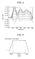
- Fig.3 is a graph showing chirping wave-shapes which change depending on each of the combinations of both the facets of the source for integrating the modulator of Fig.2.
- Fig.4 is a wave-shape diagram of a signal voltage applied to the modulator during measurement of the chirping.
- Fig.5 is a graph showing a relation between a ⁇ L value of a diffraction grating and a transmission yield.
- Fig.6 is a graph showing a relation between the ⁇ L value of the diffraction grating and the transmission yield using, as a parameter, the reflection rate of the output facet of the modulator.
- Fig.7 is a graph showing a relation between the ⁇ L value of the diffraction grating and all the yield using, as a parameter, the reflection rate of the output facet of the modulator.
- Fig.8 is a top plan view showing a resonator module in accordance with a second embodiment of the present invention.
- a distributed feedback semiconductor laser (DFB-LD) 30 and a field absorbing modulator (MOD) 40 are integrated together on a single semiconductor substrate.
- a diffraction grating 13 having a space period of 2400 ⁇ formed in a direction of progress of light and a flat phase shifting region 14 having a length of ⁇ g/4 are formed on an n-InP substrate 11 by using, for example, an electron-beam exposure method or a chemical etching method.
- the phase shifting region 14 is disposed in the diffraction grating 13 such that the ratio between distances from the rear facet and the front facet (the emission end of the semiconductor laser) to the phase shifting region is 0.3 : 0.7.
- an n-InGaAsP optical guide layer 15 having a wavelength of 1.15 ⁇ m, an undoped InGaAsP active layer 16 having a wavelength of 1.55 ⁇ m, a p-Inp cladding layer 17 and a p + -InGaAs cap layer 18 are sequentially and epitaxially grown.
- an n-InGaAsP buffer layer 20 an undoped InGaAsP light-absorbing layer 21, a p-InP cladding layer 22, and a p + -InGaAs cap layer 23 are sequentially and epitaxially stacked onto the same n-InP substrate 11 by using a selective MOVPE (Metal Organic Vapor Phase Epitaxy) method or a pad joint method.
- MOVPE Metal Organic Vapor Phase Epitaxy
- a trench 25 is formed by using an ordinal etching method for electrically isolating the modulator 40 and the DFB laser 30.
- An n-type electrode 12 and p-type electrodes 14 and 19 are formed on the multi-layered semiconductor obtained in this manner.
- an AR (anti-reflection) coat film 27 is formed on the facet of the modulator 40, and an HR (higher reflection) coat film 26 is formed on the facet of the DFB-LD 30, thereby providing the configuration of the light source integrated with the modulator of the embodiment.
- the reflection rate of the light-emitting facet of the modulator 40 (optical power reflection rate) is 0.01 %, and the ⁇ L value of the diffraction grating 13 of the DFB laser 30 is established between 1 and 1.2, wherein " ⁇ " is a mode coupling constant, and “L” is a cavity length of the DFB laser.
- a pulse voltage shown in Fig.4 was applied between the electrodes 23 and 12 of the modulator 40 to obtain the simulated change of the laser emission frequencies (chirping) as shown in Fig.3 by using a simulation.
- a plurality of curves in Fig.3 were formed depending on the combinations of the optical phases at both the facets of the light source integrated with the modulator. It can be seen from Fig.3 that the change of the combination of the optical phases at both the ends significantly changes its chirping. However, the excellent chirping can be hardly obtained if the combination of the phases at both the ends is determined by simply selecting the cavity length of the semiconductor laser.
- the chirping is a main factor dominating the transmission performance, and the degree of the chirping is changed depending on the combination of the facet phases.
- the combination of the front and rear facet phases differs from the combination of another element, and has randomness substantially uncontrollable.
- the ratio of the facet phases generating the chirping in a permitted range exhibits the transmission yield.
- a graph of Fig.5 shows the chirping from peak to peak ( ⁇ fpp), wherein simulated results (a curve 101 in the graph) of the transmission yields were obtained, and results by the actual measurement (dots 102 in the graph) were obtained under the situation that the product having the ⁇ fpp 2.5 GHz was judged to be good quality. It can be seen from the graph of Fig.5 that the simulated results and the actual results were in excellent agreement, and the transmission yield increased with the increase of the ⁇ L value of the diffraction grating. The results are illustrated in Fig.6 which were obtained by the simulation and show the dependency of the transmission yield on the ⁇ L value and the reflection rate (R) of the modulator facet. As shown in the graph, the reduction of the reflection rate (R) increases the transmission yield.
- Fig.7 All the yield changes depending on the above two main factors are shown in Fig.7, that is, the dependency of all the yields obtained by the single mode yield and the transmission yield on the ⁇ L value of the diffraction grating and the reflection rate of the modulator facet. Although only part of the reflection rates are shown in Fig.7 for facilitating the understanding, other various curves corresponding to the remaining reflection rates were obtained based on the simulations shown in Figs.1 and 6 and actual measurements. It can be understood from Figs.6 and 7 that the proper selection of the ⁇ L value and the facet reflection rate can obtain the maximum yield.
- the maximum yield can generally be obtained in the ⁇ L value range between 1 and 1.2 when the facet reflection rate (R) is 0.01 %, and can be obtained in the ⁇ L value range between 1.4 and 1.7 when the facet reflection rate (R) is 0.1 %.
- the ⁇ L value range realizing the maximum yield of the integrated source was established with respect to each of the facet reflection rates of the modulator based on the combinations of the points obtained in Figs.1 and 6.
- the ⁇ L value range is between 1.0 and 1.2 when the reflection rate is between 0.01 and 0.02 %, the ⁇ L value range is between 1.2 and 1.3 when the reflection rate is between 0.02 and 0.03 %, the ⁇ L value range is between 1.3 and 1.4 when the reflection rate is between 0.03 and 0.05 %, and the ⁇ L value range is between 1.4 and 1.7 when the reflection rate is between 0.05 and 0.1 %.
- the all the maximum yields of the integrated source can be obtained by the combinations of the proper ⁇ L value and the reflection rate.
- the modulator module 52 includes a photo-modulator 53 having substantially same configuration as that of the first embodiment and a non-spherical surface lens 54 jointly having a single optical axis with the photo-modulator 53 overlying a sub-mount 51.
- the light of the photo-modulator 53 is incident through the non-spherical surface lens 54 on an optical fiber 55 an end of which is fixed to the end of the sub-mount 51.
- the modulator module 52 of the embodiment easily forms optical modulation signals with lower chirping.
Landscapes
- Physics & Mathematics (AREA)
- Condensed Matter Physics & Semiconductors (AREA)
- General Physics & Mathematics (AREA)
- Electromagnetism (AREA)
- Optics & Photonics (AREA)
- Semiconductor Lasers (AREA)
Abstract
Description
- The present invention relates to a light source integrated with a modulator and a module for optical communication, and especially to the structure for the light source integrated with the modulator and suitable for a light source for long distance trunk used in wavelength division multiplexing (WDM).
- As a light source for long distance trunk used in WDM, a module is put into practice which includes a distributed feedback semiconductor laser (DFB-LD) and a field absorbing modulator (MOD) on a single semiconductor substrate. This type of light source can realizes the transmission speed as high as 2.5 Gb/s and has been vigorously researched.
- A resistance to distribution or an ability of transmitting long-distance signals in the DFB-LD is the most important parameter exhibiting element performance. The selection of products having no defect therein is currently conducted by measuring the resistance to distribution or the power penalty after the transmission of each element. It is an important subject to increase the yield of the selection for decreasing the cost of the light source.
- Murotani et al. reported the dependency of the single mode yield of the DFB/MOD module having an asymmetrical λ /4 phase shifter (a structure obtained by moving the λ /4 phase shift region of the diffraction grating from the central position of the DFB-LD, hereinafter referred to as "asymmetrical λ /4-DFB/MOD") on a κ L value of a diffraction grating in the DFB-LD in the Electronics Society Meeting (C-4-15, p242) held in September 1999 by the Institute of Electronics, Information and Communication Engineers.
- As shown in Fig.1, the single mode yield rapidly decreases with the increase of the κ L in the asymmetrical λ /4-DFB/MOD module. Conventional publications including the above publication describe neither the yield of the power source integrated with the modulator separately from the single mode yield, nor the optimum structure regarding determination of the facet reflection rate and of the κ L. The optimum structure has not been conventionally established by considering the dependency of the diffraction grating on the κ L value and the dependency of the modulator on the facet reflection rate.
- In view of the foregoing, an object of the present invention is to increase the yield of obtaining DFB/MOD module having no defect by considering the dependency of the □L value of the diffraction grating on the single mode yield and the transmission yield and the dependency of the modulator on the facet reflection rate.
- The present invention provides an optical device including: a substrate; a distributed feedback (DFB) semiconductor laser formed on the substrate and including a diffraction grating having an asymmetrical λ/4 phase shift region, the diffraction grating extending along an optical axis of the DFB semiconductor laser; and a field absorbing modulator integrated with the DFB semiconductor laser on the substrate for modulating a light wave emitted from the DFB semiconductor laser, the modulator having a facet reflection rate between 0.01 and 0.02 % at an output end thereof, the diffraction grating having a□L value between 1.4 and 1.7.
- In another aspect of the present invention, the facet reflection rate of the output end of the modulator is in a range between 0.02 and 0.03 %, and the κL value of the diffraction grating is between 1.2 and 1.3.
- In a further aspect of the present invention, the facet reflection rate of the output end of the modulator is in a range between 0.03 and 0.05 %, and the κ L value of the diffraction grating is between 1.3 and 1.4.
- In a still further aspect of the present invention, the facet reflection rate of the output end of the modulator is in a range between 0.05 and 0.1 %, and the κL value of the diffraction grating is between 1.4 and 1.7.
- In accordance with the present invention, the proper combinations of the κL value of the diffraction grating and the reflection rate of the output facet of the modulator of the DFB semiconductor laser can fabricate the source for integrating the modulator having the excellent quality with a higher yield and lower cost.
- The above and other objects, features and advantages of the present invention will be more apparent from the following description.
- Fig.1 is a graph showing a relation between a □L value of a diffraction grating and a single mode yield.
- Fig.2 is a vertical sectional view showing a source for integrating a modulator in accordance with a first embodiment of the present invention.
- Fig.3 is a graph showing chirping wave-shapes which change depending on each of the combinations of both the facets of the source for integrating the modulator of Fig.2.
- Fig.4 is a wave-shape diagram of a signal voltage applied to the modulator during measurement of the chirping.
- Fig.5 is a graph showing a relation between a□L value of a diffraction grating and a transmission yield.
- Fig.6 is a graph showing a relation between the □L value of the diffraction grating and the transmission yield using, as a parameter, the reflection rate of the output facet of the modulator.
- Fig.7 is a graph showing a relation between the □L value of the diffraction grating and all the yield using, as a parameter, the reflection rate of the output facet of the modulator.
- Fig.8 is a top plan view showing a resonator module in accordance with a second embodiment of the present invention.
- Then, the configuration of a light source for integrating a modulator of a first embodiment will be described referring to Fig.2.
- As shown therein, a distributed feedback semiconductor laser (DFB-LD) 30 and a field absorbing modulator (MOD) 40 are integrated together on a single semiconductor substrate. A diffraction grating 13 having a space period of 2400 Å formed in a direction of progress of light and a flat
phase shifting region 14 having a length of λ g/4 are formed on an n-InP substrate 11 by using, for example, an electron-beam exposure method or a chemical etching method. Thephase shifting region 14 is disposed in the diffraction grating 13 such that the ratio between distances from the rear facet and the front facet (the emission end of the semiconductor laser) to the phase shifting region is 0.3 : 0.7. Then, an n-InGaAsPoptical guide layer 15 having a wavelength of 1.15 µm, an undoped InGaAsPactive layer 16 having a wavelength of 1.55 µm, a p-Inp cladding layer 17 and a p+-InGaAs cap layer 18 are sequentially and epitaxially grown. Further, an n-InGaAsP buffer layer 20, an undoped InGaAsP light-absorbinglayer 21, a p-InP cladding layer 22, and a p+-InGaAs cap layer 23 are sequentially and epitaxially stacked onto the same n-InP substrate 11 by using a selective MOVPE (Metal Organic Vapor Phase Epitaxy) method or a pad joint method. - Then, a
trench 25 is formed by using an ordinal etching method for electrically isolating themodulator 40 and the DFBlaser 30. An n-type electrode 12 and p-type electrodes coat film 27 is formed on the facet of themodulator 40, and an HR (higher reflection)coat film 26 is formed on the facet of the DFB-LD 30, thereby providing the configuration of the light source integrated with the modulator of the embodiment. The reflection rate of the light-emitting facet of the modulator 40 (optical power reflection rate) is 0.01 %, and the □L value of the diffraction grating 13 of the DFBlaser 30 is established between 1 and 1.2, wherein "□" is a mode coupling constant, and "L" is a cavity length of the DFB laser. - Under the condition of continuously emitting light by the semiconductor laser at an operation current of 70 mA, a pulse voltage shown in Fig.4 was applied between the
electrodes modulator 40 to obtain the simulated change of the laser emission frequencies (chirping) as shown in Fig.3 by using a simulation. A plurality of curves in Fig.3 were formed depending on the combinations of the optical phases at both the facets of the light source integrated with the modulator. It can be seen from Fig.3 that the change of the combination of the optical phases at both the ends significantly changes its chirping. However, the excellent chirping can be hardly obtained if the combination of the phases at both the ends is determined by simply selecting the cavity length of the semiconductor laser. - The chirping is a main factor dominating the transmission performance, and the degree of the chirping is changed depending on the combination of the facet phases. The combination of the front and rear facet phases differs from the combination of another element, and has randomness substantially uncontrollable. Among the facet phases randomly occurring, the ratio of the facet phases generating the chirping in a permitted range exhibits the transmission yield.
- A graph of Fig.5 shows the chirping from peak to peak (▵fpp), wherein simulated results (a
curve 101 in the graph) of the transmission yields were obtained, and results by the actual measurement (dots 102 in the graph) were obtained under the situation that the product having the Δfpp 2.5 GHz was judged to be good quality. It can be seen from the graph of Fig.5 that the simulated results and the actual results were in excellent agreement, and the transmission yield increased with the increase of the □L value of the diffraction grating. The results are illustrated in Fig.6 which were obtained by the simulation and show the dependency of the transmission yield on the □L value and the reflection rate (R) of the modulator facet. As shown in the graph, the reduction of the reflection rate (R) increases the transmission yield. - The dependency of the single mode yield which is another main factor of increasing the yield on the □L value was measured and summarized in Fig.1.
- All the yield changes depending on the above two main factors are shown in Fig.7, that is, the dependency of all the yields obtained by the single mode yield and the transmission yield on the □L value of the diffraction grating and the reflection rate of the modulator facet. Although only part of the reflection rates are shown in Fig.7 for facilitating the understanding, other various curves corresponding to the remaining reflection rates were obtained based on the simulations shown in Figs.1 and 6 and actual measurements. It can be understood from Figs.6 and 7 that the proper selection of the □L value and the facet reflection rate can obtain the maximum yield. For example, the maximum yield can generally be obtained in the κL value range between 1 and 1.2 when the facet reflection rate (R) is 0.01 %, and can be obtained in the κL value range between 1.4 and 1.7 when the facet reflection rate (R) is 0.1 %.
- The κL value range realizing the maximum yield of the integrated source was established with respect to each of the facet reflection rates of the modulator based on the combinations of the points obtained in Figs.1 and 6. The κL value range is between 1.0 and 1.2 when the reflection rate is between 0.01 and 0.02 %, the κL value range is between 1.2 and 1.3 when the reflection rate is between 0.02 and 0.03 %, the κ L value range is between 1.3 and 1.4 when the reflection rate is between 0.03 and 0.05 %, and the κ L value range is between 1.4 and 1.7 when the reflection rate is between 0.05 and 0.1 %. In this manner, the all the maximum yields of the integrated source can be obtained by the combinations of the proper κ L value and the reflection rate.
- Then, the configuration of a modulator module for optical communication of a second embodiment will be described referring to Fig.8.
- The
modulator module 52 includes a photo-modulator 53 having substantially same configuration as that of the first embodiment and anon-spherical surface lens 54 jointly having a single optical axis with the photo-modulator 53 overlying a sub-mount 51. The light of the photo-modulator 53 is incident through thenon-spherical surface lens 54 on anoptical fiber 55 an end of which is fixed to the end of the sub-mount 51. Themodulator module 52 of the embodiment easily forms optical modulation signals with lower chirping. - Since the above embodiment is described only for examples, the present invention is not limited to the above embodiment and various modifications or alterations can be easily made therefrom by those skilled in the art without departing from the scope of the present invention.
Claims (8)
- An optical device comprising:a substrate;a distributed feedback (DFB) semiconductor laser (30) formed on the substrate (11) and including a diffraction grating (13) having an asymmetrical λ /4 phase shift region (14), the diffraction grating (13) extending along an optical axis of the DFB semiconductor laser (30); anda field absorbing modulator (40) integrated with the DFB semiconductor laser (30) on the substrate (11) for modulating a light wave emitted from the DFB semiconductor laser (30) characterized in that:
the modulator (40) has a facet reflection rate between 0.01 and 0.02 % at an output end thereof, and the diffraction grating (13) has a κ L value between 1 and 1.2. - An optical modulator comprising the optical device as defined in claim 1 as a built-in light source.
- An optical device comprising:a substrate;a distributed feedback (DFB) semiconductor laser (30) formed on the substrate (11) and including a diffraction grating (13) having an asymmetrical λ /4 phase shift region (14), the diffraction grating (13) extending along an optical axis of the DFB semiconductor laser (30); anda field absorbing modulator (40) integrated with the DFB semiconductor laser (30) on the substrate (11) for modulating a light wave emitted from the DFB semiconductor laser (30) characterized in that:
the modulator (40) has a facet reflection rate between 0.02 and 0.03 % at an output end thereof, and the diffraction grating (13) has a κ L value between 1.2 and 1.3. - An optical modulator comprising the optical device as defined in claim 3 as a built-in light source.
- An optical device comprising:a substrate;a distributed feedback (DFB) semiconductor laser (30) formed on the substrate (11) and including a diffraction grating (13) having an asymmetrical λ /4 phase shift region (14), the diffraction grating (13) extending along an optical axis of the DFB semiconductor laser (30); anda field absorbing modulator (40) integrated with the DFB semiconductor laser (30) on the substrate (11) for modulating a light wave emitted from the DFB semiconductor laser (30) characterized in that:
the modulator (40) has a facet reflection rate between 0.03 and 0.05 % at an output end thereof, and the diffraction grating (13) has a κL value between 1.3 and 1.4. - An optical modulator comprising the optical device as defined in claim 5 as a built-in light source.
- An optical device comprising:a substrate;a distributed feedback (DFB) semiconductor laser (30) formed on the substrate (11) and including a diffraction grating (13) having an asymmetrical λ /4 phase shift region (14), the diffraction grating (13) extending along an optical axis of the DFB semiconductor laser (30); anda field absorbing modulator (40) integrated with the DFB semiconductor laser (30) on the substrate (11) for modulating a light wave emitted from the DFB semiconductor laser (30) characterized in that:
the modulator (40) has a facet reflection rate between 0.05 and 0.1 % at an output end thereof, and the diffraction grating (13) has a κL value between 1.4 and 1.7. - An optical modulator comprising the optical device as defined in claim 7 as a built-in light source.
Applications Claiming Priority (2)
| Application Number | Priority Date | Filing Date | Title |
|---|---|---|---|
| JP2000136137 | 2000-05-09 | ||
| JP2000136137A JP2001320124A (en) | 2000-05-09 | 2000-05-09 | Modulator integrated light source and module for optical communication |
Publications (1)
| Publication Number | Publication Date |
|---|---|
| EP1154533A1 true EP1154533A1 (en) | 2001-11-14 |
Family
ID=18644126
Family Applications (1)
| Application Number | Title | Priority Date | Filing Date |
|---|---|---|---|
| EP01111372A Withdrawn EP1154533A1 (en) | 2000-05-09 | 2001-05-09 | Light source containing a distributed feedback laser and an integrated optical modulator |
Country Status (4)
| Country | Link |
|---|---|
| US (1) | US6646775B2 (en) |
| EP (1) | EP1154533A1 (en) |
| JP (1) | JP2001320124A (en) |
| CA (1) | CA2346596A1 (en) |
Cited By (2)
| Publication number | Priority date | Publication date | Assignee | Title |
|---|---|---|---|---|
| US11251585B2 (en) * | 2019-10-01 | 2022-02-15 | Ii-Vi Delaware, Inc. | DFB with weak optical feedback |
| CN114175427A (en) * | 2019-08-02 | 2022-03-11 | 三菱电机株式会社 | Semiconductor laser device |
Families Citing this family (20)
| Publication number | Priority date | Publication date | Assignee | Title |
|---|---|---|---|---|
| US9372306B1 (en) | 2001-10-09 | 2016-06-21 | Infinera Corporation | Method of achieving acceptable performance in and fabrication of a monolithic photonic integrated circuit (PIC) with integrated arrays of laser sources and modulators employing an extended identical active layer (EIAL) |
| US10012797B1 (en) | 2002-10-08 | 2018-07-03 | Infinera Corporation | Monolithic photonic integrated circuit (PIC) with a plurality of integrated arrays of laser sources and modulators employing an extended identical active layer (EIAL) |
| JP3641473B2 (en) | 2002-10-25 | 2005-04-20 | 沖電気工業株式会社 | Optical semiconductor device |
| JP4639578B2 (en) | 2003-06-27 | 2011-02-23 | 日本電気株式会社 | Semiconductor laser module and manufacturing method thereof |
| KR100809412B1 (en) | 2005-12-07 | 2008-03-05 | 한국전자통신연구원 | Electro-absorption Modulator integrated laser and method of manufacturing the same |
| JP2007227560A (en) * | 2006-02-22 | 2007-09-06 | Mitsubishi Electric Corp | Gain-coupled distributed feedback semiconductor laser |
| US8238759B2 (en) * | 2008-02-14 | 2012-08-07 | Infinera Corporation | High capacity transmitter implemented on a photonic integrated circuit |
| US20100290489A1 (en) * | 2009-05-15 | 2010-11-18 | Avago Technologies Fiber Ip (Singapore) Pte. Ltd. | electro-absorption modulated laser (eml) assembly having a 1/4 wavelength phase shift located in the forward portion of the distributed feedback (dfb) of the eml assembly, and a method |
| US20110134957A1 (en) * | 2009-12-07 | 2011-06-09 | Emcore Corporation | Low Chirp Coherent Light Source |
| KR20130085498A (en) * | 2011-12-12 | 2013-07-30 | 한국전자통신연구원 | Multichannel transmitter optical module |
| US9306672B2 (en) | 2013-03-14 | 2016-04-05 | Encore Corporation | Method of fabricating and operating an optical modulator |
| US9306372B2 (en) | 2013-03-14 | 2016-04-05 | Emcore Corporation | Method of fabricating and operating an optical modulator |
| US9059801B1 (en) | 2013-03-14 | 2015-06-16 | Emcore Corporation | Optical modulator |
| JP6291849B2 (en) * | 2014-01-10 | 2018-03-14 | 三菱電機株式会社 | Semiconductor device manufacturing method, semiconductor device |
| US9564733B2 (en) | 2014-09-15 | 2017-02-07 | Emcore Corporation | Method of fabricating and operating an optical modulator |
| ITUB20160994A1 (en) * | 2016-02-23 | 2017-08-23 | Prima Electro S P A | LASER SEMICONDUCTOR DIODE AND PROCEDURE FOR ITS REALIZATION |
| US10074959B2 (en) | 2016-08-03 | 2018-09-11 | Emcore Corporation | Modulated laser source and methods of its fabrication and operation |
| JP6673137B2 (en) * | 2016-10-18 | 2020-03-25 | 三菱電機株式会社 | Semiconductor laser device with optical modulator |
| KR102191374B1 (en) * | 2016-11-22 | 2020-12-16 | 한국전자통신연구원 | Optical transmitter module |
| JP2022506323A (en) * | 2018-11-05 | 2022-01-17 | 華為技術有限公司 | Externally reflected return light resistant laser |
Family Cites Families (3)
| Publication number | Priority date | Publication date | Assignee | Title |
|---|---|---|---|---|
| JP2749038B2 (en) * | 1987-07-31 | 1998-05-13 | 株式会社日立製作所 | Tunable semiconductor laser |
| JP3307905B2 (en) * | 1999-12-28 | 2002-07-29 | 日本電気株式会社 | Optical semiconductor device and method of manufacturing the same |
| JP3339488B2 (en) * | 2000-02-25 | 2002-10-28 | 日本電気株式会社 | Optical semiconductor device and method of manufacturing the same |
-
2000
- 2000-05-09 JP JP2000136137A patent/JP2001320124A/en active Pending
-
2001
- 2001-05-08 US US09/850,115 patent/US6646775B2/en not_active Expired - Lifetime
- 2001-05-08 CA CA002346596A patent/CA2346596A1/en not_active Abandoned
- 2001-05-09 EP EP01111372A patent/EP1154533A1/en not_active Withdrawn
Non-Patent Citations (5)
| Title |
|---|
| AOKI M ET AL: "NEW TRANSMISSION SIMULATION OF EA-MODULATOR INTEGRATED DFB-LASERS CONSIDERING THE FACET REFLECTION-INDUCED CHIRP", IEEE PHOTONICS TECHNOLOGY LETTERS,US,IEEE INC. NEW YORK, vol. 9, no. 3, 1 March 1997 (1997-03-01), pages 380 - 382, XP000684419, ISSN: 1041-1135 * |
| JUN-ICHI HASHIMOTO ET AL: "INFLUENCE OF FACET REFLECTION ON THE PERFORMANCE OF A DFB LASER INTEGRATED WITH AN OPTICAL AMPLIFIER/MODULATOR", IEEE JOURNAL OF QUANTUM ELECTRONICS,US,IEEE INC. NEW YORK, vol. 28, no. 3, 1 March 1992 (1992-03-01), pages 594 - 603, XP000271768, ISSN: 0018-9197 * |
| KOTAKI Y ET AL: "ANALYSIS OF STATIC AND DYNAMIC WAVELENGTH SHIFTS IN MODULATOR INTEGRATED DFB LASERS", PROCEEDINGS OF THE EUROPEAN CONFERENCE ON OPTICAL COMMUNICATION (ECOC),CH,ZURICH, SEV, vol. CONF. 19, 12 September 1993 (1993-09-12), pages 381 - 384, XP000492242 * |
| SAHLEN O: "OPTIMIZATION OF DFB LASERS INTEGRATED WITH FRANZ-KELDYSH ABSOPRTIONMODULATORS", JOURNAL OF LIGHTWAVE TECHNOLOGY,US,IEEE. NEW YORK, vol. 12, no. 6, 1 June 1994 (1994-06-01), pages 969 - 976, XP000484213, ISSN: 0733-8724 * |
| YAMAGUCHI M ET AL: "REQUIREMENTS FOR MODULATOR-INTEGRATED DFB LD'S FOR PENALTY-FREE 2.5-GB/S TRANSMISSION", JOURNAL OF LIGHTWAVE TECHNOLOGY,US,IEEE. NEW YORK, vol. 13, no. 10, 1 October 1995 (1995-10-01), pages 1948 - 1954, XP000596072, ISSN: 0733-8724 * |
Cited By (4)
| Publication number | Priority date | Publication date | Assignee | Title |
|---|---|---|---|---|
| CN114175427A (en) * | 2019-08-02 | 2022-03-11 | 三菱电机株式会社 | Semiconductor laser device |
| CN114175427B (en) * | 2019-08-02 | 2024-04-19 | 三菱电机株式会社 | Semiconductor laser device |
| US11251585B2 (en) * | 2019-10-01 | 2022-02-15 | Ii-Vi Delaware, Inc. | DFB with weak optical feedback |
| US12494619B2 (en) | 2019-10-01 | 2025-12-09 | Ii-Vi Delaware, Inc. | DFB with weak optical feedback |
Also Published As
| Publication number | Publication date |
|---|---|
| US20010043384A1 (en) | 2001-11-22 |
| CA2346596A1 (en) | 2001-11-09 |
| US6646775B2 (en) | 2003-11-11 |
| JP2001320124A (en) | 2001-11-16 |
Similar Documents
| Publication | Publication Date | Title |
|---|---|---|
| US6646775B2 (en) | Light source for integrating modulator and module for optical communication | |
| EP0173269B1 (en) | Semiconductor laser device | |
| EP0814547B1 (en) | Semiconductor laser and process for producing the same | |
| JPH11505965A (en) | DFB laser diode structure with complex optical grating coupling | |
| JPH0256837B2 (en) | ||
| JPH09283841A (en) | Distributed feedback semiconductor laser device, manufacturing method thereof, and exposure method | |
| EP0125608A2 (en) | Single longitudinal mode semiconductor laser | |
| US4701930A (en) | Distributed feedback semiconductor laser | |
| US4794608A (en) | Semiconductor laser device | |
| JP5243901B2 (en) | Coaxial type semiconductor optical module | |
| US4794618A (en) | Distributed feedback laser diode | |
| US6917055B2 (en) | Optoelectronic component and method for producing an optoelectronic component | |
| US6825505B2 (en) | Phase-shifted distributed feedback type semiconductor laser diode capable of improving wavelength chirping and external reflection return light characteristics | |
| JP2012002929A (en) | Method for manufacturing semiconductor optical element, laser module, and optical transmission apparatus | |
| EP0772267A1 (en) | Laser diode device | |
| JP3778260B2 (en) | Semiconductor laser and digital optical communication system and method using the same | |
| EP4122062B1 (en) | Electroabsorption modulated laser | |
| US6018540A (en) | Semiconductor light emitting element and optical fiber transmission system | |
| KR20180069717A (en) | Semiconductor laser, light source unit, communication system, and wavelength division multiplexing optical communication system | |
| JPH0529602A (en) | Semiconductor optical integrated device and manufacturing method thereof | |
| EP1065765A2 (en) | Optical semiconductor device and optical communication system | |
| JP3700245B2 (en) | Phase-shifted distributed feedback semiconductor laser | |
| JP6673137B2 (en) | Semiconductor laser device with optical modulator | |
| EP0257898A2 (en) | External resonator type semiconductor laser | |
| JPH08274406A (en) | Distributed feedback semiconductor laser device and manufacturing method thereof |
Legal Events
| Date | Code | Title | Description |
|---|---|---|---|
| PUAI | Public reference made under article 153(3) epc to a published international application that has entered the european phase |
Free format text: ORIGINAL CODE: 0009012 |
|
| AK | Designated contracting states |
Kind code of ref document: A1 Designated state(s): AT BE CH CY DE DK ES FI FR GB GR IE IT LI LU MC NL PT SE TR Kind code of ref document: A1 Designated state(s): DE FR GB IT |
|
| AX | Request for extension of the european patent |
Free format text: AL;LT;LV;MK;RO;SI |
|
| 17P | Request for examination filed |
Effective date: 20020114 |
|
| AKX | Designation fees paid |
Free format text: DE FR GB IT |
|
| RAP1 | Party data changed (applicant data changed or rights of an application transferred) |
Owner name: NEC ELECTRONICS CORPORATION |
|
| STAA | Information on the status of an ep patent application or granted ep patent |
Free format text: STATUS: THE APPLICATION HAS BEEN WITHDRAWN |
|
| 18W | Application withdrawn |
Effective date: 20031223 |