EP1154532A2 - Self-mode-locking quantum cascade laser - Google Patents
Self-mode-locking quantum cascade laser Download PDFInfo
- Publication number
- EP1154532A2 EP1154532A2 EP01303946A EP01303946A EP1154532A2 EP 1154532 A2 EP1154532 A2 EP 1154532A2 EP 01303946 A EP01303946 A EP 01303946A EP 01303946 A EP01303946 A EP 01303946A EP 1154532 A2 EP1154532 A2 EP 1154532A2
- Authority
- EP
- European Patent Office
- Prior art keywords
- quantum cascade
- laser
- cascade laser
- region
- mode
- Prior art date
- Legal status (The legal status is an assumption and is not a legal conclusion. Google has not performed a legal analysis and makes no representation as to the accuracy of the status listed.)
- Granted
Links
Images




Classifications
-
- H—ELECTRICITY
- H01—ELECTRIC ELEMENTS
- H01S—DEVICES USING THE PROCESS OF LIGHT AMPLIFICATION BY STIMULATED EMISSION OF RADIATION [LASER] TO AMPLIFY OR GENERATE LIGHT; DEVICES USING STIMULATED EMISSION OF ELECTROMAGNETIC RADIATION IN WAVE RANGES OTHER THAN OPTICAL
- H01S5/00—Semiconductor lasers
- H01S5/30—Structure or shape of the active region; Materials used for the active region
- H01S5/34—Structure or shape of the active region; Materials used for the active region comprising quantum well or superlattice structures, e.g. single quantum well [SQW] lasers, multiple quantum well [MQW] lasers or graded index separate confinement heterostructure [GRINSCH] lasers
- H01S5/3401—Structure or shape of the active region; Materials used for the active region comprising quantum well or superlattice structures, e.g. single quantum well [SQW] lasers, multiple quantum well [MQW] lasers or graded index separate confinement heterostructure [GRINSCH] lasers having no PN junction, e.g. unipolar lasers, intersubband lasers, quantum cascade lasers
- H01S5/3402—Structure or shape of the active region; Materials used for the active region comprising quantum well or superlattice structures, e.g. single quantum well [SQW] lasers, multiple quantum well [MQW] lasers or graded index separate confinement heterostructure [GRINSCH] lasers having no PN junction, e.g. unipolar lasers, intersubband lasers, quantum cascade lasers intersubband lasers, e.g. transitions within the conduction or valence bands
-
- B—PERFORMING OPERATIONS; TRANSPORTING
- B82—NANOTECHNOLOGY
- B82Y—SPECIFIC USES OR APPLICATIONS OF NANOSTRUCTURES; MEASUREMENT OR ANALYSIS OF NANOSTRUCTURES; MANUFACTURE OR TREATMENT OF NANOSTRUCTURES
- B82Y20/00—Nanooptics, e.g. quantum optics or photonic crystals
-
- H—ELECTRICITY
- H01—ELECTRIC ELEMENTS
- H01S—DEVICES USING THE PROCESS OF LIGHT AMPLIFICATION BY STIMULATED EMISSION OF RADIATION [LASER] TO AMPLIFY OR GENERATE LIGHT; DEVICES USING STIMULATED EMISSION OF ELECTROMAGNETIC RADIATION IN WAVE RANGES OTHER THAN OPTICAL
- H01S5/00—Semiconductor lasers
- H01S5/06—Arrangements for controlling the laser output parameters, e.g. by operating on the active medium
- H01S5/065—Mode locking; Mode suppression; Mode selection ; Self pulsating
-
- H—ELECTRICITY
- H01—ELECTRIC ELEMENTS
- H01S—DEVICES USING THE PROCESS OF LIGHT AMPLIFICATION BY STIMULATED EMISSION OF RADIATION [LASER] TO AMPLIFY OR GENERATE LIGHT; DEVICES USING STIMULATED EMISSION OF ELECTROMAGNETIC RADIATION IN WAVE RANGES OTHER THAN OPTICAL
- H01S5/00—Semiconductor lasers
- H01S5/06—Arrangements for controlling the laser output parameters, e.g. by operating on the active medium
- H01S5/065—Mode locking; Mode suppression; Mode selection ; Self pulsating
- H01S5/0657—Mode locking, i.e. generation of pulses at a frequency corresponding to a roundtrip in the cavity
-
- H—ELECTRICITY
- H01—ELECTRIC ELEMENTS
- H01S—DEVICES USING THE PROCESS OF LIGHT AMPLIFICATION BY STIMULATED EMISSION OF RADIATION [LASER] TO AMPLIFY OR GENERATE LIGHT; DEVICES USING STIMULATED EMISSION OF ELECTROMAGNETIC RADIATION IN WAVE RANGES OTHER THAN OPTICAL
- H01S5/00—Semiconductor lasers
- H01S5/20—Structure or shape of the semiconductor body to guide the optical wave ; Confining structures perpendicular to the optical axis, e.g. index or gain guiding, stripe geometry, broad area lasers, gain tailoring, transverse or lateral reflectors, special cladding structures, MQW barrier reflection layers
- H01S5/22—Structure or shape of the semiconductor body to guide the optical wave ; Confining structures perpendicular to the optical axis, e.g. index or gain guiding, stripe geometry, broad area lasers, gain tailoring, transverse or lateral reflectors, special cladding structures, MQW barrier reflection layers having a ridge or stripe structure
- H01S5/2205—Structure or shape of the semiconductor body to guide the optical wave ; Confining structures perpendicular to the optical axis, e.g. index or gain guiding, stripe geometry, broad area lasers, gain tailoring, transverse or lateral reflectors, special cladding structures, MQW barrier reflection layers having a ridge or stripe structure comprising special burying or current confinement layers
- H01S5/2214—Structure or shape of the semiconductor body to guide the optical wave ; Confining structures perpendicular to the optical axis, e.g. index or gain guiding, stripe geometry, broad area lasers, gain tailoring, transverse or lateral reflectors, special cladding structures, MQW barrier reflection layers having a ridge or stripe structure comprising special burying or current confinement layers based on oxides or nitrides
-
- H—ELECTRICITY
- H01—ELECTRIC ELEMENTS
- H01S—DEVICES USING THE PROCESS OF LIGHT AMPLIFICATION BY STIMULATED EMISSION OF RADIATION [LASER] TO AMPLIFY OR GENERATE LIGHT; DEVICES USING STIMULATED EMISSION OF ELECTROMAGNETIC RADIATION IN WAVE RANGES OTHER THAN OPTICAL
- H01S5/00—Semiconductor lasers
- H01S5/20—Structure or shape of the semiconductor body to guide the optical wave ; Confining structures perpendicular to the optical axis, e.g. index or gain guiding, stripe geometry, broad area lasers, gain tailoring, transverse or lateral reflectors, special cladding structures, MQW barrier reflection layers
- H01S5/22—Structure or shape of the semiconductor body to guide the optical wave ; Confining structures perpendicular to the optical axis, e.g. index or gain guiding, stripe geometry, broad area lasers, gain tailoring, transverse or lateral reflectors, special cladding structures, MQW barrier reflection layers having a ridge or stripe structure
- H01S5/2205—Structure or shape of the semiconductor body to guide the optical wave ; Confining structures perpendicular to the optical axis, e.g. index or gain guiding, stripe geometry, broad area lasers, gain tailoring, transverse or lateral reflectors, special cladding structures, MQW barrier reflection layers having a ridge or stripe structure comprising special burying or current confinement layers
- H01S5/2214—Structure or shape of the semiconductor body to guide the optical wave ; Confining structures perpendicular to the optical axis, e.g. index or gain guiding, stripe geometry, broad area lasers, gain tailoring, transverse or lateral reflectors, special cladding structures, MQW barrier reflection layers having a ridge or stripe structure comprising special burying or current confinement layers based on oxides or nitrides
- H01S5/2216—Structure or shape of the semiconductor body to guide the optical wave ; Confining structures perpendicular to the optical axis, e.g. index or gain guiding, stripe geometry, broad area lasers, gain tailoring, transverse or lateral reflectors, special cladding structures, MQW barrier reflection layers having a ridge or stripe structure comprising special burying or current confinement layers based on oxides or nitrides nitrides
-
- H—ELECTRICITY
- H01—ELECTRIC ELEMENTS
- H01S—DEVICES USING THE PROCESS OF LIGHT AMPLIFICATION BY STIMULATED EMISSION OF RADIATION [LASER] TO AMPLIFY OR GENERATE LIGHT; DEVICES USING STIMULATED EMISSION OF ELECTROMAGNETIC RADIATION IN WAVE RANGES OTHER THAN OPTICAL
- H01S5/00—Semiconductor lasers
- H01S5/20—Structure or shape of the semiconductor body to guide the optical wave ; Confining structures perpendicular to the optical axis, e.g. index or gain guiding, stripe geometry, broad area lasers, gain tailoring, transverse or lateral reflectors, special cladding structures, MQW barrier reflection layers
- H01S5/22—Structure or shape of the semiconductor body to guide the optical wave ; Confining structures perpendicular to the optical axis, e.g. index or gain guiding, stripe geometry, broad area lasers, gain tailoring, transverse or lateral reflectors, special cladding structures, MQW barrier reflection layers having a ridge or stripe structure
- H01S5/227—Buried mesa structure ; Striped active layer
- H01S5/2275—Buried mesa structure ; Striped active layer mesa created by etching
Definitions
- the present invention relates to a quantum cascade laser and, more particularly, to a quantum cascade laser structure that is capable of self-mode-locking behavior in the mid-infrared wavelength range.
- ultrafast laser sources that is, sources capable of generating optical pulses with durations ranging from a few picoseconds down into the femtosecond range.
- Some of these ultrashort pulses have been generated in a variety of gas and solid-state laser media. These sources have allowed for a dramatic improvement in the temporal resolution of a myriad of measurements in physics, chemistry and biology.
- the need for increased bandwidth in optical communications is another factor influencing the design and development of ultrafast laser sources.
- Ultrafast semiconductor lasers are particularly important for telecommunications applications, given their compact size, high efficiency, low cost and unmatched pulse repetition rates (up to a few hundred of GHz).
- mode-locking results from a periodic modulation of the laser gain with the fundamental period equal to the cavity roundtrip time. Under these conditions, maximum gain is experienced by a laser beam consisting of a train of pulses, separated by the roundtrip time, and properly synchronized with the modulation.
- An optical waveform with these characteristics is established through the coherent addition of several longitudinal modes of the laser cavity, when the modes are phase-locked to one another. The characteristics of such a device are often described in the frequency domain. In this description, when the laser is modulated at the cavity roundtrip frequency (i.e., the frequency separation between adjacent modes), several modes are driven above threshold by the modulation sidebands of their neighbors, which automatically establishes the phase-locking required for pulsed laser emission.
- the modulation responsible for mode-locking may be produced by an external source (defined as “active” mode-locking), or by the laser pulses themselves through some intracavity optical nonlinearity (defined as “passive”, or “self' mode-locking).
- active mode-locking an external source
- passive an intracavity optical nonlinearity
- the shortest pulse durations and the largest repetition rates can be obtained with self-mode-locking (SML) and several techniques of SML have been demonstrated over the past few years.
- SML self-mode-locking
- a nonlinear mechanism is required that reduces the losses with an increasing optical power.
- One exemplary arrangement is an intracavity saturable absorber; that is, an absorber whose opacity at the laser wavelength decreases with increasing intensity.
- a nonlinear mirror or a nonlinear coupled-cavity may be used.
- Another effective mechanism, discovered in association with Ti:sapphire lasers, is self-focusing or Kerr-lensing, which requires an intracavity medium with a positive nonlinear refractive index. That is, a refractive index that increases with increasing intensity.
- the center part of the beam transverse profile experiences a larger index, and is therefore slowed down in its propagation relative to the edges.
- the nonlinear medium acts as a positive lens narrowing the beam diameter, to an extent proportional to the optical power; this effect can then be converted into a saturable loss mechanism simply by using an intracavity slit or aperture.
- the loss recovers from saturation on an "ultrafast" time scale, in particular, on a time scale that is much faster than the cavity roundtrip time.
- the losses must quickly return to their steady-state (relatively high) value before the arrival of the next pulse, so as to prevent light emissions between consecutive pulses.
- the relaxation lifetime of the SML nonlinearity also limits the resulting optical pulse widths.
- an "intrinsic" nonlinear refractive index is present in any laser medium, provided by the lasing transition itself and related to the gain coefficient through a Kramers-Kronig transformation.
- This is a resonant nonlinearity, and therefore inherently large, so that one may expect that, combined with the appropriate cavity configuration (e.g., a coupled-cavity system, or an intracavity aperture), a laser medium with a sufficiently large intrinsic nonlinear refractive index could be used to provide a self-mode-locking laser.
- the appropriate cavity configuration e.g., a coupled-cavity system, or an intracavity aperture
- a laser medium with a sufficiently large intrinsic nonlinear refractive index could be used to provide a self-mode-locking laser.
- the lifetime of the upper laser state In mode-locked lasers developed to date, this lifetime is much slower than (or comparable to) the cavity roundtrip time, and therefore fails to satisfy the above-mentioned requirements for SML.
- mode-locked lasers of the prior art have been limited to an "extrinsic" structure, requiring the use of an externally added non-linearity, or loss “discriminator” to provide the mode locking capability.
- the use of one or more external components increases both the cost and complexity of the mode-locked laser system.
- the present invention relates to a self-mode locking laser and, more particularly, to a quantum cascade laser structure that is capable of self-mode-locking behavior in the mid-infrared wavelength range.
- quantum cascade lasers characterized by intersubband transitions having large index nonlinearities (due to their extremely large dipole moments) are used to generate picoseconds pulses of mid-infrared light.
- Kerr-lens mode-locking of a QC laser is provided by the index nonlinearity of the intersubband lasing transition.
- the intracavity aperture required to convert the QC self-focusing mechanism into a loss modulation is provided by a QC laser waveguide that is characterized by: (1) an optically highly lossy (i.e., absorbing) layer (such as a metal, for example), separated from the semiconductor material by a relatively thin dielectric layer such that it "sees” (i.e., optically interacts with) the optical wave formed in the active region; and (2) a relatively long laser waveguide (such that the propagation losses dominate over other losses, such as mirror losses).
- the highly lossy layer used for mode coupling can comprise a metal and be disposed to also form one of the electrical contacts for the laser device.
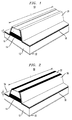
- FIG. 1 An isometric view of an exemplary QC laser 10 capable of self-mode-locked (SML) operation is illustrated in FIG. 1.
- QC laser 10 comprises an active region 14 sandwiched between an upper cladding region 16 and a lower cladding region 12. At least upper cladding region 16 and active region 14 have the shape of an elongated mesa typical of ridge waveguide laser structures.
- An electrical insulating layer 18 (for example, silicon nitride or silicon dioxide) is formed over the top of the device and is patterned to form an opening which exposes a portion of the top of the mesa.
- a top side metal contact 20 is formed to coat insulating layer 18, as well as to cover the exposed portion of upper cladding region 16.
- a second electrode 22 is formed across the bottom surface of substrate 11.
- Substrate 11 itself may be a single crystal semiconductor body or a combination of such a body with another layer (e.g., an epitaxial layer grown on the top surface of the body).
- layers of this type are fabricated from Group III-V compound semiconductors; e.g., In-based Group III-V compounds such as GaInAs and AlInAs.
- the laser beam is primarily confined by the cladding regions 12,16 immediately surrounding active region 14.
- a strong confinement of the beam can be achieved by forming cladding regions 12,16 such that they have a first high-refractive index layer (such as low doped InGaAs) adjacent to active region 14, followed by a second low-refractive index material layer (such as InAlAs or InP)
- a first high-refractive index layer such as low doped InGaAs
- a second low-refractive index material layer such as InAlAs or InP
- insulating layer 18 must be relatively thin (e.g., a thickness, denoted t , of less than 0.5 ⁇ m). The relatively thin layer is required for the optical wave within active region 14 to "see” (i.e., optically interact with) metal layer 20, thus providing mode coupling to metal layer 20. However, insulating layer 18 must not be so thin so as to allow for a direct electrical path to be formed between metal layer 20 and active region 14 (that is, insulating layer 18 must be thick enough to prevent the formation of an electrical short in the device). Second, the extent of the waveguide ridge, denoted "L" in FIG. 1, is required to be relatively long (for example, ⁇ 3.5 mm), so that propagation losses will dominate over mirror losses. It has been found, as will be discussed in detail below, that the combination of these two characteristics leads to self-mode locking in QC lasers.
- L the extent of the waveguide ridge
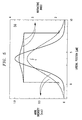
- FIG. 2 An alternative embodiment 30 of the present invention is illustrated in FIG. 2, where in this arrangement, a separate top electrical contact 32 and highly optically lossy sidewall layers 34,36 are used. Sidewall layers 34,36 are disposed as shown to cover thin insulating layer 18 in the region of interest surrounding active region 14. Top electrical contact 32 is disposed in the opening created in insulating layer 18 and provides for the direct electrical contact to upper cladding layer 16. In general, since these layers perform different functions, they may comprise different thicknesses, or even different compositions. For the purposes of the present invention, the layers of concern are sidewall layers 34,36 which are required to provide mode coupling to the optical wave within active region 14. As with the arrangement of FIG.
- the thickness t of insulating layer 18 must be well-controlled such that mode coupling will occur, and the length of the waveguide must by sufficient to insure that self-mode-locking will take place. It is to be noted that in the particular situation where the highly lossy sidewall layers are themselves electrically insulating, a separate insulator 18 will not be required and that aspect incorporated directly into the lossy sidewall layers.
- highly optically lossy sidewall layers 34,36 may comprise metal layers (such as gold, for example), and may even comprise the same material as top contact 32 and deposited on the sidewalls during the same processing step.
- highly optically lossy layers 34, 36 may comprise any suitable (i.e., lossy or absorbing) material. That is, any material capable of providing sufficient mode coupling in the lateral direction and loss for the light guided in the waveguide.
- suitable materials such as polyimide
- polyimide are generally known to exhibit a strong resonant absorption in the mid-infrared wavelength range.
- QC lasers consist of several (usually between 25 and 30) repeat units of radiative transition regions (termed 'active region" in FIG. 3) and injector regions such as illustrated in FIG. 3, stacked in series in a cascade configuration to form active region 14.
- the laser material is grown by molecular beam epitaxy in a InGaAs/AlInAs material system that is lattice-matched to a low-doped InP substrate (such as substrate 11). It is then processed by wet chemical etching into the mesa structure as shown in FIGs. 1 and 2.
- QC laser action is based on intersubband electron transitions, i.e., transitions between quantized conduction-band states in coupled quantum-wells.
- a distinctive feature of these transitions is their ultrafast relaxation times, typically a few picoseconds, which is at least two orders of magnitude faster than in all other laser systems.
- the electronic band structure of a conventional QC laser active region i.e. radiative transition region
- FIG. 3 Essentially, it comprises a three-level system, where carriers are injected into the upper state (labeled "3" in FIG. 3) by tunneling through a thin heterostructure barrier, and extracted from the lower laser state (labeled "2”) by LO phonon-assisted scattering into state 1.
- phonon emission is also extremely effective in depopulating upper state 3, thereby resulting in picoseconds carrier lifetimes (much shorter than the typical roundtrip times in QC lasers, which are on the order of several tens of picoseconds).
- intersubband transitions are characterized by giant index nonlinearities, due to their extremely large dipole moments.
- these transitions are used to generate picoseconds pulses of mid-infrared light.
- Kerr-lens mode-locking of a QC laser is achieved, resulting from the index nonlinearity of the intersubband lasing transitions.
- the intracavity aperture required to convert the self-focusing mechanism into a loss modulation is provided by the QC laser waveguide under the conditions defined above, namely, the use of a relatively thin dielectric overlaid by a strongly absorbing (i.e., highly optically lossy) material, and a long waveguide region.
- SML QC lasers of the present invention are also suitable for use in high-speed free-space communication systems, given the low atmospheric losses of mid-infrared light.
- FIG. 4 illustrates both the refractive index profile and resulting intensity distribution in the transverse direction of the fundamental mode of an exemplary QC laser as depicted in FIGs. 1 and 2.
- self-focusing does not occur in the transverse direction, since the mode is primarily confined by the cladding layers surrounding the active material (i.e., the regions of highest index in FIG. 4), where no such strong nonlinearity exists.
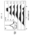
- FIG. 5 illustrates the refractive index profile and resulting intensity distribution along the lateral direction of the same device (i.e., parallel to the active layer). Self-focusing occurs in the lateral direction as a result of the strong index nonlinearity of the active region, as shown.
- the waveguiding results mainly from the difference between the effective index of the semiconductor stack (i.e., the combination of regions 12,14 and 16) and the complex index of the overlying dielectric and optically lossy layers.
- the semiconductor stack has a large contribution from the gain medium itself (active region 14), and is therefore highly nonlinear. Consequently, as shown in FIG. 5, an increase in optical power leads to a focusing of the laser beam via the Kerr effect. The increase in optical power then causes a larger overlap with the gain region, and a reduced overlap with the lossy external absorbing (e.g., metal) layers, thereby producing the saturable loss mechanism required for self-mode locking.
- this nonlinear contribution needs to be the primary portion of the overall cavity losses in the QC device. Accordingly, the use of a relatively thin dielectric (i.e., ⁇ 0.5 ⁇ m) between the semiconductor material and the metal sidewall layers ensures that there will be sufficient mode coupling to the metal.
- Gold is one exemplary metal that may be used for this purpose.
- a relatively long cavity e.g., L > 3.5mm is also a necessity.
- the individual lasers were then wire bonded, soldered to a copper heat sink, and mounted on a temperature-controlled cold finger of a helium flow cryostat.
- the light output from these devices was detected with a fast (12 GHz nominal bandwidth), quantum well infrared photodetector (QWIP), mounted inside a liquid-nitrogen dewar.
- Optical spectral measurements were performed with a Fourier transform infrared spectrometer (FTIR).
- the interference fringes making up these traces can only occur when the pulses from the two arms of the interferometer temporally overlap on the detector. Therefore, the negligible amplitude of the fringes observed in FIGs. 7A and B for large delay times between the two arms indicates pulsed emission with a good modulation depth. It is to be noted, however, that these traces cannot provide an accurate measurement of the duration of the pulses since they are affected by their phase as well as amplitude.
- the pulse width can, however, be estimated from the multi-peaked structures observed in the optical spectra (directly related to the side lobes in the autocorrelation traces of FIG. 7), using a procedure first outlined in an article entitled "Optical Pulsewidth Measurement Using Self-Phase Modulation", by C.H. Lin et al. , appearing in IEEE J. of Quantum Electronics, Vol. 8, 1972, beginning at page 429.
- these multi-peaked structures are a signature of self-phase modulation, which can be described as the temporal analog of self-focusing. That is, in the presence of a quadratic index nonlinearity, the optical field develops a time-varying phase proportional to the pulse intensity profile.
- ⁇ max is the root-mean square spectral width
- ⁇ p is the full-width at half-maximum (FWHM) pulse width
- FWHM full-width at half-maximum
- L is the propagation length (in this case, the laser roundtrip path)
- ⁇ is the wavelength
- n 2 is the nonlinear index
- I max is the pulse peak intensity.
- a slow pyroelectric detector can be used to measure the L-I characteristics of an SML QC device (i.e., average optical power versus bias current).
- the transition from cw to SML operation can be seen in the curves of FIG. 8, in the form of a sudden increase in the slope efficiency dL/dI.
- the peak power of the pulses can be estimated, given the knowledge of their width and repetition rate. In general, the peak encompasses values ranging from a few hundreds of milliwatts to well over a watt, depending on the operating conditions.
- the far-field beam profile can be measured and compared under both cw vs. SML operation.
- a measurement was taken using a QC laser in which SML was found to be non self-starting.
- This particular device exhibited single-mode cw emission at 8 ⁇ m when biased with a dc current.
- Mode-locking was achieved by superimposing an rf modulation on the dc bias that was resonant with its roundtrip frequency (as in active mode locking). However, the laser then remained in the mode-locked state, even after the modulation was switched off.
- This device was particularly well-suited for this measurement since it allowed for the comparison of two cases (i.e., cw and self-starting) under the same conditions of bias, temperature, etc. It was found that the far-field beam profile under SML conditions was broader than in cw, corresponding to a narrower beam inside the waveguide. Therefore, at the higher instantaneous power levels inherent to pulsed emission, the beam does undergo self-focusing inside the laser.
- the ratio in beam diameter between the cw and SML cases was found to increase with dc bias (and hence, optical power), and it was measured to be as large as 1.33.
- nonresonant processes such as two-photon absorption, electronic Raman scattering, and optical Stark effect, which have been observed to produce a Kerr nonlinearity in semiconductors, can all be ruled out as sources, since their resulting nonlinearities are too weak (n 2 ⁇ 10 -12 cm 2 /W, or smaller).
- the nonlinear index of the laser intersubband transition it can be calculated from the following expression that is based on a two-level approximation: where z 32 is the dipole moment of the lasing transition, ⁇ N is the population inversion per unit volume, n is the background refractive index, ⁇ 0 and ⁇ are the center frequency and the FWHM of the gain curve, I sat is the saturation intensity, and q, ⁇ 0 , and h are the unit charge, vacuum permittivity, and Planck's constant, respectively.
- z 32 is the dipole moment of the lasing transition
- ⁇ N the population inversion per unit volume
- n the background refractive index
- ⁇ 0 and ⁇ are the center frequency and the FWHM of the gain curve
- I sat is the saturation intensity
- q, ⁇ 0 , and h are the unit charge, vacuum permittivity, and Planck's constant, respectively.
- n 2 has the value of zero at the gain center frequency ⁇ 0 , which is a general property of the Kramers-Kronig transform of a symmetrical function.
- ⁇ 0 is a general property of the Kramers-Kronig transform of a symmetrical function.
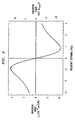
- n 2 is already large enough (approximately 10 -9 cm 2 /W) to justify the experimental findings.
- the right axis of FIG. 9 was scaled to display ⁇ max versus ⁇ , using equation (2) with parameter values corresponding to the spectrum of FIG. 5 at 600 mA.
- the phase shift ⁇ max 3/2 ⁇ , required to explain the spectral shapes of FIG. 6, is reached at a detuning of less than 100 GHz.
- the relaxation lifetime of this nonlinearity given by the lifetime of the laser population inversion, is a few picoseconds (by design), which is consistent with the measured pulse widths.
Landscapes
- Physics & Mathematics (AREA)
- Optics & Photonics (AREA)
- Engineering & Computer Science (AREA)
- Condensed Matter Physics & Semiconductors (AREA)
- General Physics & Mathematics (AREA)
- Electromagnetism (AREA)
- Nanotechnology (AREA)
- Chemical & Material Sciences (AREA)
- Biophysics (AREA)
- Crystallography & Structural Chemistry (AREA)
- Life Sciences & Earth Sciences (AREA)
- Semiconductor Lasers (AREA)
- Lasers (AREA)
Abstract
Description


Claims (19)
- A quantum cascade (QC) laser comprising a multilayer structure forming an optical structure, said structure comprisingCHARACTERIZED IN THATa core region of relatively large effective refractive index disposed between cladding regions of relatively small effective refractive index, the core region comprising a multiplicity of nominally identical repeat units, each repeat unit comprising an active region (radiative transition region) and a carrier injection region, the active region having a layer structure selected to provide an upper and a lower carrier energy state, such that a carrier transition from the upper to the lower energy state results in emission of a photon of wavelength λ, the carrier injection region having a layer structure selected to facilitate carrier transport from the lower energy state of the active region of a given repeat unit to the upper energy state of the active region of an adjacent downstream repeat unit;top and bottom cladding regions disposed on either side of said core region, wherein at least said top cladding region and said core region form a mesa structurean insulating layer covering exposed surfaces of said cladding layers and said core region; andelectrical contacts attached to the top and bottom cladding layers for facilitating the flow of electric current through the laserthe quantum cascade laser is self-mode-locking, whereinthe insulating layer comprises comprising a relatively thin layer of less than a micron in depth, and the quantum cascade laser further comprisesoptically lossy sidewall layers disposed to cover said relatively thin layer in at least the area of said active region, said quantum cascade laser further comprising a relatively long active region cavity, sufficient for propagation losses to be greater than mirror losses
- A quantum cascade laser as defined in claim 1 wherein the laser is self-mode locking and comprises an insulating layer less than 0.5 microns in depth
- A quantum cascade laser as defined in claim 1 wherein the insulating layer comprises silicon nitride
- A quantum cascade laser as defined in claim 1 wherein the insulating layer comprises silicon dioxide.
- A quantum cascade laser as defined in claim 1 wherein the laser emits an output wavelength in the mid-infrared region
- A quantum cascade laser as defined in claim 5 wherein the laser emits at a wavelength of approximately 5 µm.
- A quantum cascade laser as defined in claim 5 wherein the laser emits at a wavelength of approximately 8 µm.
- A quantum cascade laser as defined in claim 1 wherein each pulse output is of a relatively narrow pulse width.
- A quantum cascade laser as defined in claim 8 wherein the pulse width is less than five picoseconds
- A quantum cascade laser as defined in claim 1 wherein the optically lossy sidewall layers comprise a metal material and form a continuous layer with a top electrical contact to the upper cladding region
- A quantum cascade laser as defined in claim 10 wherein the metal material comprises gold.
- A quantum cascade laser as defined in claim 1 wherein the optically lossy sidewall layers are separate from the top electrical contact.
- A quantum cascade laser as defined in claim 12 wherein the optically lossy sidewall layers comprise metallic layers.
- A quantum cascade laser as defined in claim 13 wherein the sidewall metallic layers comprise the same material as the top electrical contact.
- A quantum cascade laser as defined in claim 14 wherein the sidewall metallic layers and the top electric contact comprise gold.
- A quantum cascade laser as defined in claim 12 wherein the optically lossy sidewall layers comprise polymeric substances.
- A quantum cascade laser as defined in claim 1 wherein the upper and lower cladding regions comprise a plurality of InGaAs/AlInAs epitaxial layers.
- A quantum cascade laser as defined in claim 1 wherein the relatively long active region cavity comprises a length ≥ 3.5mm.
- A quantum cascade laser as defined in claim 1 wherein the optically lossy layers are electrically insulating and incorporate the insulating layer.
Applications Claiming Priority (2)
| Application Number | Priority Date | Filing Date | Title |
|---|---|---|---|
| US566348 | 2000-05-08 | ||
| US09/566,348 US6563852B1 (en) | 2000-05-08 | 2000-05-08 | Self-mode-locking quantum cascade laser |
Publications (3)
| Publication Number | Publication Date |
|---|---|
| EP1154532A2 true EP1154532A2 (en) | 2001-11-14 |
| EP1154532A3 EP1154532A3 (en) | 2004-01-02 |
| EP1154532B1 EP1154532B1 (en) | 2005-10-26 |
Family
ID=24262501
Family Applications (1)
| Application Number | Title | Priority Date | Filing Date |
|---|---|---|---|
| EP01303946A Expired - Lifetime EP1154532B1 (en) | 2000-05-08 | 2001-04-30 | Self-mode-locking quantum cascade laser |
Country Status (6)
| Country | Link |
|---|---|
| US (1) | US6563852B1 (en) |
| EP (1) | EP1154532B1 (en) |
| JP (1) | JP3785057B2 (en) |
| CN (1) | CN1326300C (en) |
| CA (1) | CA2342080C (en) |
| DE (1) | DE60114286T2 (en) |
Cited By (10)
| Publication number | Priority date | Publication date | Assignee | Title |
|---|---|---|---|---|
| FR2833419A1 (en) * | 2001-12-07 | 2003-06-13 | Thales Sa | SINGLE POLE LASER WITH QUANTUM POWER CASCADE WITH REDUCED THRESHOLD CURRENT |
| GB2385462A (en) * | 2002-02-15 | 2003-08-20 | Denselight Semiconductors Pte | A semiconductor laser structure |
| DE10205310A1 (en) * | 2002-02-08 | 2003-09-18 | Fraunhofer Ges Forschung | Laser device with a quantum cascade laser |
| WO2005001511A1 (en) * | 2003-06-13 | 2005-01-06 | Cubic Corporation | Integrated optical communication and range finding system and applications thereof |
| DE102005022436A1 (en) * | 2005-05-14 | 2006-11-23 | Universität Konstanz | Saturable absorber for lasers |
| WO2007053336A1 (en) * | 2005-10-28 | 2007-05-10 | Lucent Technologies Inc. | Self-mode-locked semiconductor laser |
| WO2009070821A3 (en) * | 2007-12-05 | 2009-08-06 | Univ Wien Tech | Semiconductor laser having absorption layer |
| US8051597B1 (en) | 2007-06-14 | 2011-11-08 | Cubic Corporation | Scout sniper observation scope |
| CN102623872A (en) * | 2012-03-23 | 2012-08-01 | 中国科学院紫金山天文台 | Quantum cascade laser (QCL) phase-locked system using solid-state semiconductor source harmonic as reference source |
| US9068798B2 (en) | 2010-07-19 | 2015-06-30 | Cubic Corporation | Integrated multifunction scope for optical combat identification and other uses |
Families Citing this family (28)
| Publication number | Priority date | Publication date | Assignee | Title |
|---|---|---|---|---|
| US6584245B1 (en) * | 1996-05-06 | 2003-06-24 | Teracomm Research, Inc | High speed data link including a superconductive plate assembly for use in a data transmission scheme and method |
| JP3532838B2 (en) | 2000-08-30 | 2004-05-31 | 独立行政法人 科学技術振興機構 | Ultrashort pulse light source |
| JP2002111135A (en) * | 2000-10-02 | 2002-04-12 | Furukawa Electric Co Ltd:The | Semiconductor laser device and pump light source for optical fiber amplifier using the same |
| US20020097471A1 (en) * | 2001-01-22 | 2002-07-25 | Bethea Clyde George | Data transmission via direct modulation of a mid-IR laser |
| JP2003017804A (en) * | 2001-07-04 | 2003-01-17 | Fuji Photo Film Co Ltd | Semiconductor laser device and manufacturing method thereof |
| AU2003284468A1 (en) * | 2002-11-27 | 2004-06-18 | Jaidan Hojin Handotai Kenkyu Shinkokai | Electromagnetic wave applicator |
| US7301977B2 (en) * | 2004-06-10 | 2007-11-27 | Nanoplus Gmbh | Tuneable unipolar lasers |
| JP4536490B2 (en) * | 2004-11-15 | 2010-09-01 | 浜松ホトニクス株式会社 | Laser apparatus and control method thereof |
| CN100373723C (en) * | 2005-08-31 | 2008-03-05 | 中国科学院上海微系统与信息技术研究所 | Quality control method for atomic layer scale epitaxy materials based on indium phosphide-based quantum cascade lasers |
| JP2008060396A (en) * | 2006-08-31 | 2008-03-13 | Hamamatsu Photonics Kk | Quantum cascade laser |
| US7993124B2 (en) * | 2006-12-28 | 2011-08-09 | The Boeing Company | Heating apparatus for a composite laminator and method |
| US20110058176A1 (en) * | 2008-11-03 | 2011-03-10 | Bruker Optics, Inc. | Spectrometers utilizing mid infrared ultra broadband high brightness light sources |
| US7940818B2 (en) * | 2009-01-13 | 2011-05-10 | The University Of Maryland, Baltimore County | Passively mode locked quantum cascade lasers |
| CN101916965B (en) * | 2010-07-14 | 2011-12-07 | 中国科学院半导体研究所 | Short-wavelength grating surface emission quantum cascade laser structure and preparation method thereof |
| JP5729138B2 (en) | 2011-05-30 | 2015-06-03 | 住友電気工業株式会社 | Manufacturing method of optical semiconductor device |
| US9088126B2 (en) | 2013-10-17 | 2015-07-21 | The Trustees Of Princeton University | Single-mode quantum cascade lasers with enhanced tuning range |
| JP6269091B2 (en) * | 2014-01-17 | 2018-01-31 | 住友電気工業株式会社 | Semiconductor optical device manufacturing method |
| JP6379696B2 (en) | 2014-06-05 | 2018-08-29 | 住友電気工業株式会社 | Quantum cascade laser diode |
| JP6145080B2 (en) * | 2014-09-29 | 2017-06-07 | 三菱重工業株式会社 | Laser oscillation cooling device |
| JP6485340B2 (en) | 2015-12-09 | 2019-03-20 | 住友電気工業株式会社 | Method for fabricating quantum cascade laser, quantum cascade laser |
| JP2018026440A (en) | 2016-08-09 | 2018-02-15 | 住友電気工業株式会社 | Integrated quantum cascade laser, semiconductor optical device |
| JP6965545B2 (en) * | 2017-03-30 | 2021-11-10 | 住友電気工業株式会社 | Optical semiconductor device |
| US10084282B1 (en) | 2017-08-14 | 2018-09-25 | The United States Of America As Represented By The Secretary Of The Air Force | Fundamental mode operation in broad area quantum cascade lasers |
| US11031753B1 (en) * | 2017-11-13 | 2021-06-08 | The Government Of The United States Of America As Represented By The Secretary Of The Air Force | Extracting the fundamental mode in broad area quantum cascade lasers |
| CN108458995B (en) * | 2018-05-09 | 2020-07-21 | 长江师范学院 | Quantitative determination method for stimulated conversion of abundance-rigidity-degree-order-life of phonon characteristic of chemical bond |
| CN115224587B (en) * | 2022-08-19 | 2025-06-13 | 中国科学院半导体研究所 | Quantum cascade laser active area unit, active area, epitaxial structure and chip |
| CN119674711B (en) * | 2024-12-05 | 2025-09-12 | 安徽格恩半导体有限公司 | A semiconductor laser element with a quantum confined Stark control layer |
| CN121558683A (en) * | 2026-01-26 | 2026-02-24 | 合肥清芯传感科技有限公司 | TDLAS linear parameter dynamic correction method based on environment parameter real-time feedback |
Family Cites Families (17)
| Publication number | Priority date | Publication date | Assignee | Title |
|---|---|---|---|---|
| DE3234389C2 (en) * | 1982-09-16 | 1995-03-09 | Siemens Ag | Semiconductor laser diode |
| JPH0254596A (en) * | 1988-08-18 | 1990-02-23 | Mitsubishi Electric Corp | Semiconductor laser |
| US5079772A (en) * | 1990-12-21 | 1992-01-07 | Coherent, Inc. | Mode-locked laser using non-linear self-focusing element |
| JP2746065B2 (en) * | 1993-07-29 | 1998-04-28 | 日本電気株式会社 | Method for manufacturing optical semiconductor device |
| US5570386A (en) * | 1994-04-04 | 1996-10-29 | Lucent Technologies Inc. | Semiconductor laser |
| US5509025A (en) * | 1994-04-04 | 1996-04-16 | At&T Corp. | Unipolar semiconductor laser |
| US5457709A (en) | 1994-04-04 | 1995-10-10 | At&T Ipm Corp. | Unipolar semiconductor laser |
| US5727010A (en) | 1996-03-20 | 1998-03-10 | Lucent Technologies Inc. | Article comprising an improved quantum cascade laser |
| US5696784A (en) * | 1996-04-19 | 1997-12-09 | Opto Power Corporation | Reduced mode laser and method of fabrication |
| JP2822994B2 (en) | 1996-09-11 | 1998-11-11 | 日本電気株式会社 | Mode-locked semiconductor laser |
| US5936989A (en) | 1997-04-29 | 1999-08-10 | Lucent Technologies, Inc. | Quantum cascade laser |
| JPH10233556A (en) * | 1997-02-20 | 1998-09-02 | Mitsubishi Electric Corp | Ridge type semiconductor laser diode and method of manufacturing the same |
| US5901168A (en) | 1997-05-07 | 1999-05-04 | Lucent Technologies Inc. | Article comprising an improved QC laser |
| JPH1168231A (en) * | 1997-08-25 | 1999-03-09 | Mitsubishi Electric Corp | Semiconductor laser and method of manufacturing the same |
| US6055257A (en) | 1998-04-27 | 2000-04-25 | Lucent Technologies Inc. | Quantum cascade laser |
| US6301282B1 (en) * | 1998-07-29 | 2001-10-09 | Lucent Technologies Inc. | Long wavelength semiconductor lasers incorporating waveguides based on surface plasmons |
| US6055254A (en) | 1998-09-23 | 2000-04-25 | Lucent Technologies Inc. | Quantum cascade light emitter with pre-biased internal electronic potential |
-
2000
- 2000-05-08 US US09/566,348 patent/US6563852B1/en not_active Expired - Lifetime
-
2001
- 2001-03-27 CA CA002342080A patent/CA2342080C/en not_active Expired - Fee Related
- 2001-04-28 CN CNB011174412A patent/CN1326300C/en not_active Expired - Fee Related
- 2001-04-30 DE DE60114286T patent/DE60114286T2/en not_active Expired - Lifetime
- 2001-04-30 EP EP01303946A patent/EP1154532B1/en not_active Expired - Lifetime
- 2001-05-07 JP JP2001136193A patent/JP3785057B2/en not_active Expired - Fee Related
Cited By (17)
| Publication number | Priority date | Publication date | Assignee | Title |
|---|---|---|---|---|
| WO2003049243A3 (en) * | 2001-12-07 | 2004-02-19 | Thales Sa | Unipolar quantum cascade power laser with reduced current threshold |
| FR2833419A1 (en) * | 2001-12-07 | 2003-06-13 | Thales Sa | SINGLE POLE LASER WITH QUANTUM POWER CASCADE WITH REDUCED THRESHOLD CURRENT |
| US7983565B2 (en) | 2002-02-01 | 2011-07-19 | Cubic Corporation | Integrated optical communication and range finding system and application thereof |
| US7489865B2 (en) | 2002-02-01 | 2009-02-10 | Cubic Corporation | Integrated optical communication and range finding system and applications thereof |
| US7720388B2 (en) | 2002-02-01 | 2010-05-18 | Cubic Corporation | Integrated optical communication and range finding system and application thereof |
| DE10205310B4 (en) * | 2002-02-08 | 2010-04-15 | Fraunhofer-Gesellschaft zur Förderung der angewandten Forschung e.V. | A method for generating the effect of a broadband incoherent LED-like light source and use of such a method in a gas measuring device and in a lighting device |
| DE10205310A1 (en) * | 2002-02-08 | 2003-09-18 | Fraunhofer Ges Forschung | Laser device with a quantum cascade laser |
| GB2385462A (en) * | 2002-02-15 | 2003-08-20 | Denselight Semiconductors Pte | A semiconductor laser structure |
| WO2005001511A1 (en) * | 2003-06-13 | 2005-01-06 | Cubic Corporation | Integrated optical communication and range finding system and applications thereof |
| DE102005022436A1 (en) * | 2005-05-14 | 2006-11-23 | Universität Konstanz | Saturable absorber for lasers |
| WO2007053336A1 (en) * | 2005-10-28 | 2007-05-10 | Lucent Technologies Inc. | Self-mode-locked semiconductor laser |
| US7362787B2 (en) | 2005-10-28 | 2008-04-22 | Lucent Technologies Inc. | Self-mode-locked semiconductor laser |
| US8051597B1 (en) | 2007-06-14 | 2011-11-08 | Cubic Corporation | Scout sniper observation scope |
| WO2009070821A3 (en) * | 2007-12-05 | 2009-08-06 | Univ Wien Tech | Semiconductor laser having absorption layer |
| US9068798B2 (en) | 2010-07-19 | 2015-06-30 | Cubic Corporation | Integrated multifunction scope for optical combat identification and other uses |
| CN102623872A (en) * | 2012-03-23 | 2012-08-01 | 中国科学院紫金山天文台 | Quantum cascade laser (QCL) phase-locked system using solid-state semiconductor source harmonic as reference source |
| CN102623872B (en) * | 2012-03-23 | 2014-07-02 | 中国科学院紫金山天文台 | Quantum cascade laser (QCL) phase-locked system using solid-state semiconductor source harmonic as reference source |
Also Published As
| Publication number | Publication date |
|---|---|
| EP1154532A3 (en) | 2004-01-02 |
| JP3785057B2 (en) | 2006-06-14 |
| JP2001320136A (en) | 2001-11-16 |
| CA2342080C (en) | 2005-01-04 |
| CN1326300C (en) | 2007-07-11 |
| CA2342080A1 (en) | 2001-11-08 |
| DE60114286D1 (en) | 2005-12-01 |
| CN1323083A (en) | 2001-11-21 |
| DE60114286T2 (en) | 2006-07-13 |
| US6563852B1 (en) | 2003-05-13 |
| EP1154532B1 (en) | 2005-10-26 |
Similar Documents
| Publication | Publication Date | Title |
|---|---|---|
| EP1154532B1 (en) | Self-mode-locking quantum cascade laser | |
| Capasso et al. | New frontiers in quantum cascade lasers and applications | |
| Capasso et al. | Quantum cascade lasers: ultrahigh-speed operation, optical wireless communication, narrow linewidth, and far-infrared emission | |
| Hofstetter et al. | Demonstration of high-performance 10.16 μm quantum cascade distributed feedback lasers fabricated without epitaxial regrowth | |
| Paiella et al. | Monolithic active mode locking of quantum cascade lasers | |
| US7158545B2 (en) | Terahertz lasers and amplifiers based on resonant optical phonon scattering to achieve population inversion | |
| US7382806B2 (en) | THz semiconductor laser incorporating a controlled plasmon confinement waveguide | |
| Thompson et al. | Colliding-pulse modelocked quantum dot lasers | |
| Hou et al. | Photonic integrated circuits for terahertz source generation | |
| US20050058166A1 (en) | Metal waveguides for mode confinement in terahertz lasers and amplifiers | |
| Krakowski et al. | Stabilized high pulse energy passively mode-locked monolithic and external cavity tapered lasers for space applications | |
| Tourrenc et al. | Cross-correlation timing jitter measurement of high power passively mode-locked two-section quantum-dot lasers | |
| Prziwarka et al. | Generation of optical picosecond pulses with monolithic colliding‐pulse mode‐locked lasers containing a chirped double‐quantum‐well active region | |
| Kitada et al. | Room-temperature two-color lasing by current injection into a GaAs/AlGaAs coupled multilayer cavity fabricated by wafer bonding | |
| Jaidl | Towards broadband terahertz quantum cascade ring laser frequency combs | |
| Curwen | Development of Terahertz Quantum-Cascade VECSELs | |
| Kacmoli | Quantum Cascade Ring Laser Systems | |
| Tandoi | Monolithic high power mode locked GaAs/AlGaAs quantum well lasers | |
| Merghem et al. | Coherence collapse in monolithic quantum-dash-based passive mode-locked lasers | |
| Zia et al. | Monolithic $2\mu\mathrm {m} $ GaSb-based passively mode-locked laser | |
| Latkowski | Radio frequency and terahertz signals generated by passively mode-locked semiconductor lasers | |
| Tierno | Laser sources and nonlinear optics based on self-assembled quantum dots | |
| Richardson et al. | Solid-state repetition-rate tunable semiconductor colliding-pulse mode-locked laser | |
| Ahmad et al. | Active and hybrid modelocking of a high power (100 mW) monolithic semiconductor laser at 1550 nm | |
| Bradley et al. | Mode-locked semiconductor lasers and their spectroscopic applications |
Legal Events
| Date | Code | Title | Description |
|---|---|---|---|
| PUAI | Public reference made under article 153(3) epc to a published international application that has entered the european phase |
Free format text: ORIGINAL CODE: 0009012 |
|
| AK | Designated contracting states |
Kind code of ref document: A2 Designated state(s): AT BE CH CY DE DK ES FI FR GB GR IE IT LI LU MC NL PT SE TR |
|
| AX | Request for extension of the european patent |
Free format text: AL;LT;LV;MK;RO;SI |
|
| PUAL | Search report despatched |
Free format text: ORIGINAL CODE: 0009013 |
|
| AK | Designated contracting states |
Kind code of ref document: A3 Designated state(s): AT BE CH CY DE DK ES FI FR GB GR IE IT LI LU MC NL PT SE TR |
|
| AX | Request for extension of the european patent |
Extension state: AL LT LV MK RO SI |
|
| 17P | Request for examination filed |
Effective date: 20040621 |
|
| AKX | Designation fees paid |
Designated state(s): DE FR GB |
|
| GRAP | Despatch of communication of intention to grant a patent |
Free format text: ORIGINAL CODE: EPIDOSNIGR1 |
|
| GRAS | Grant fee paid |
Free format text: ORIGINAL CODE: EPIDOSNIGR3 |
|
| GRAA | (expected) grant |
Free format text: ORIGINAL CODE: 0009210 |
|
| AK | Designated contracting states |
Kind code of ref document: B1 Designated state(s): DE FR GB |
|
| REG | Reference to a national code |
Ref country code: GB Ref legal event code: FG4D |
|
| REF | Corresponds to: |
Ref document number: 60114286 Country of ref document: DE Date of ref document: 20051201 Kind code of ref document: P |
|
| ET | Fr: translation filed | ||
| PLBE | No opposition filed within time limit |
Free format text: ORIGINAL CODE: 0009261 |
|
| STAA | Information on the status of an ep patent application or granted ep patent |
Free format text: STATUS: NO OPPOSITION FILED WITHIN TIME LIMIT |
|
| 26N | No opposition filed |
Effective date: 20060727 |
|
| REG | Reference to a national code |
Ref country code: GB Ref legal event code: 732E Free format text: REGISTERED BETWEEN 20131031 AND 20131106 |
|
| REG | Reference to a national code |
Ref country code: FR Ref legal event code: CD Owner name: ALCATEL-LUCENT USA INC. Effective date: 20131122 |
|
| REG | Reference to a national code |
Ref country code: FR Ref legal event code: GC Effective date: 20140410 |
|
| REG | Reference to a national code |
Ref country code: FR Ref legal event code: RG Effective date: 20141015 |
|
| REG | Reference to a national code |
Ref country code: FR Ref legal event code: PLFP Year of fee payment: 15 |
|
| REG | Reference to a national code |
Ref country code: FR Ref legal event code: PLFP Year of fee payment: 16 |
|
| REG | Reference to a national code |
Ref country code: FR Ref legal event code: PLFP Year of fee payment: 17 |
|
| PGFP | Annual fee paid to national office [announced via postgrant information from national office to epo] |
Ref country code: FR Payment date: 20170419 Year of fee payment: 17 Ref country code: GB Payment date: 20170419 Year of fee payment: 17 Ref country code: DE Payment date: 20170419 Year of fee payment: 17 |
|
| REG | Reference to a national code |
Ref country code: DE Ref legal event code: R119 Ref document number: 60114286 Country of ref document: DE |
|
| GBPC | Gb: european patent ceased through non-payment of renewal fee |
Effective date: 20180430 |
|
| PG25 | Lapsed in a contracting state [announced via postgrant information from national office to epo] |
Ref country code: DE Free format text: LAPSE BECAUSE OF NON-PAYMENT OF DUE FEES Effective date: 20181101 |
|
| REG | Reference to a national code |
Ref country code: GB Ref legal event code: 732E Free format text: REGISTERED BETWEEN 20190131 AND 20190206 |
|
| PG25 | Lapsed in a contracting state [announced via postgrant information from national office to epo] |
Ref country code: GB Free format text: LAPSE BECAUSE OF NON-PAYMENT OF DUE FEES Effective date: 20180430 |
|
| PG25 | Lapsed in a contracting state [announced via postgrant information from national office to epo] |
Ref country code: FR Free format text: LAPSE BECAUSE OF NON-PAYMENT OF DUE FEES Effective date: 20180430 |